

Page 1

DC-DC converter regulated 5 V charge pump
Features
■ Regulated 5 V ±4 % charge pump
■ Output current guaranteed over temperature:
20 mA (V
■ No inductors; very low EMI noise
■ Uses small, inexpensive capacitors
■ Logic controlled 1 µA max shut-down supply
current
■ Shut down disconnects load from input
■ Available in SO-8 and DIP-8 packages
≥ 2 V), 30 mA (VI ≥ 3 V)
I
ST619LB
SO-8
Description
The ST619LB is a step-up charge pump DC-DC
converter which delivers a regulated 5 V ±4 %
output at 30 mA and over temperature. The input
voltage range is 2 V to 3.6 V (two battery cells).
It requires only four external capacitor: two
0.22 µF flying capacitors, and 10 µF capacitors at
the input and output.
Low operating supply current (typ. 200 µA) make
the device ideal for small, portable and battery
powered applications. When shut down the load
is disconnected from the input and the supply
current is typically 0.02 µA. The ST619LB is
available in SO-8 package.
Table 1. Device summary
Order codes SO-8 (tape & reel)
ST619LB ST619LBDR
November 2007 Rev. 4 1/16
www.st.com
16
Page 2

ST619LB
Contents
1 Schematic . . . . . . . . . . . . . . . . . . . . . . . . . . . . . . . . . . . . . . . . . . . . . . . . . 3
2 Pin configuration . . . . . . . . . . . . . . . . . . . . . . . . . . . . . . . . . . . . . . . . . . . 4
3 Operating principle . . . . . . . . . . . . . . . . . . . . . . . . . . . . . . . . . . . . . . . . . . 5
3.1 Shut down mode . . . . . . . . . . . . . . . . . . . . . . . . . . . . . . . . . . . . . . . . . . . . 5
4 Maximum ratings . . . . . . . . . . . . . . . . . . . . . . . . . . . . . . . . . . . . . . . . . . . . 6
5 Electrical characteristics . . . . . . . . . . . . . . . . . . . . . . . . . . . . . . . . . . . . . 7
6 Typical performance characteristics . . . . . . . . . . . . . . . . . . . . . . . . . . . . 8
7 Application information . . . . . . . . . . . . . . . . . . . . . . . . . . . . . . . . . . . . . 10
7.1 Charge pump capacitors C1 and C2 . . . . . . . . . . . . . . . . . . . . . . . . . . . . 10
7.2 Input and output capacitors C3 and C4 . . . . . . . . . . . . . . . . . . . . . . . . . . 10
7.3 Layout consideration . . . . . . . . . . . . . . . . . . . . . . . . . . . . . . . . . . . . . . . . 10
8 Package mechanical data . . . . . . . . . . . . . . . . . . . . . . . . . . . . . . . . . . . . 12
9 Revision history . . . . . . . . . . . . . . . . . . . . . . . . . . . . . . . . . . . . . . . . . . . 15
2/16
Page 3

ST619LB Schematic
1 Schematic
Figure 1. Schematic diagram
3/16
Page 4

Pin configuration ST619LB
2 Pin configuration
Figure 2. Pin connections (top view)
Table 2. Pin description
Pin n° Symbol Name and function
1 C1+ Positive terminal for the first charge pump capacitor
2 IN Input supply voltage
3 OUT 5V output voltage. V
4 C2+ Positive terminal for the second charge pump capacitor
5 C2- Negative terminal for the second charge pump capacitor
6 GND Ground
7 SHDN
8 C1- Negative terminal for the first charge pump capacitor
Active high C-MOS logic level shutdown input. SHDN is connected to GND for normal
operation.
=0V when in shutdown mode.
O
4/16
Page 5

ST619LB Operating principle
3 Operating principle
The ST619LB is able to provide a regulated 5 V output from a 2 V to 3.6 V (two battery cells)
input. Internal charge pump and external capacitors generate the 5 V output, eliminating the
need for inductors. The output voltage is regulated to 5 V, ±4 % by a pulse skipping
controller that turns on the charge pump when the output voltage begins to drop. To
maintain the greatest efficiency the internal charge pump of the device operates as a
voltage doubler when V
from 2.0 V to 2.5 V.
ranges from 3.0 V to 3.6 V and as a voltage triple when VI ranges
I
When V
ranges from 2.5 V to 3.0 V, the ST619LB switches between doubler and triple
I
mode on alternating cycles, making a 2.5 x V
efficiency over the input range, an internal comparator selects the higher of V
the ST619LB's circuitry. With V
In triple mode (see block diagram), when the S1 switches close, the S2 switches open and
capacitors C1 and C2 charge up to V
connected in series between IN and OUT when the S1 switches open and S2 switches
close. In the doubler mode only C2 is used. During one oscillator cycle, energy is transferred
from the input to the charge pump capacitors, and then from the charge pump capacitors to
the output capacitors and load. The number of cycles within a given time frame increases as
the load increases or as the input supply voltage decreases. In the limiting case, the charge
pumps operate continuously, and the oscillator frequency is nominally 500 kHz.
3.1 Shut down mode
The ST619LB enters low power shut down mode when SHDN is a logic high. In shut down
mode, OUT is disconnected from the IN and V
ground for normal operation. SHDN is a CMOS compatible input.
charge pump. To further enhance the
I
= 2 V and IO = 20 mA the typical efficiency value is 80%.
I
. On the second half of the cycle, C1 and C2 are
I
falls to 0V. The SHDN pin is connected to
O
or VO to run
I
5/16
Page 6
Maximum ratings ST619LB
4 Maximum ratings
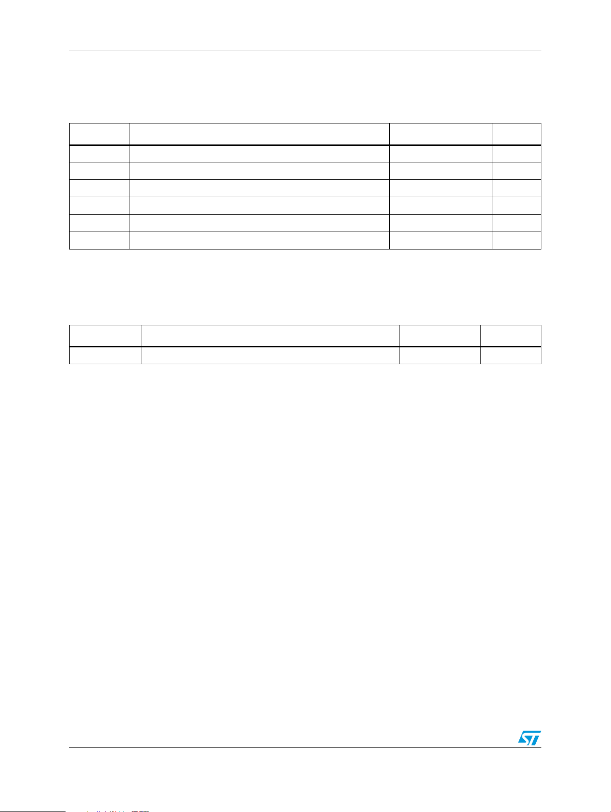
Table 3. Absolute maximum ratings
Symbol Parameter Value Unit
V
SHDN
T
T
V
V
I
O
STG
OP
I
O
DC input voltage -0.3 to 5.5 V
Output voltage -0.3 to 5.5 V
Shutdown input voltage -0.3 to (VI + 0.3) V
Output current continuous 120 mA
Storage temperature range -55 to +150 °C
Operating junction temperature range -40 to +85 °C
Note: Absolute maximum ratings are those values beyond which damage to the device may occur.
Functional operation under these condition is not implied.
Table 4. Thermal data
Symbol Parameter SO-8 Unit
R
thJA
1. This value depends from thermal design of PCB on which the device is mounted.
Thermal resistance junction-ambient
(1)
160 °C/W
6/16
Page 7
ST619LB Electrical characteristics
5 Electrical characteristics
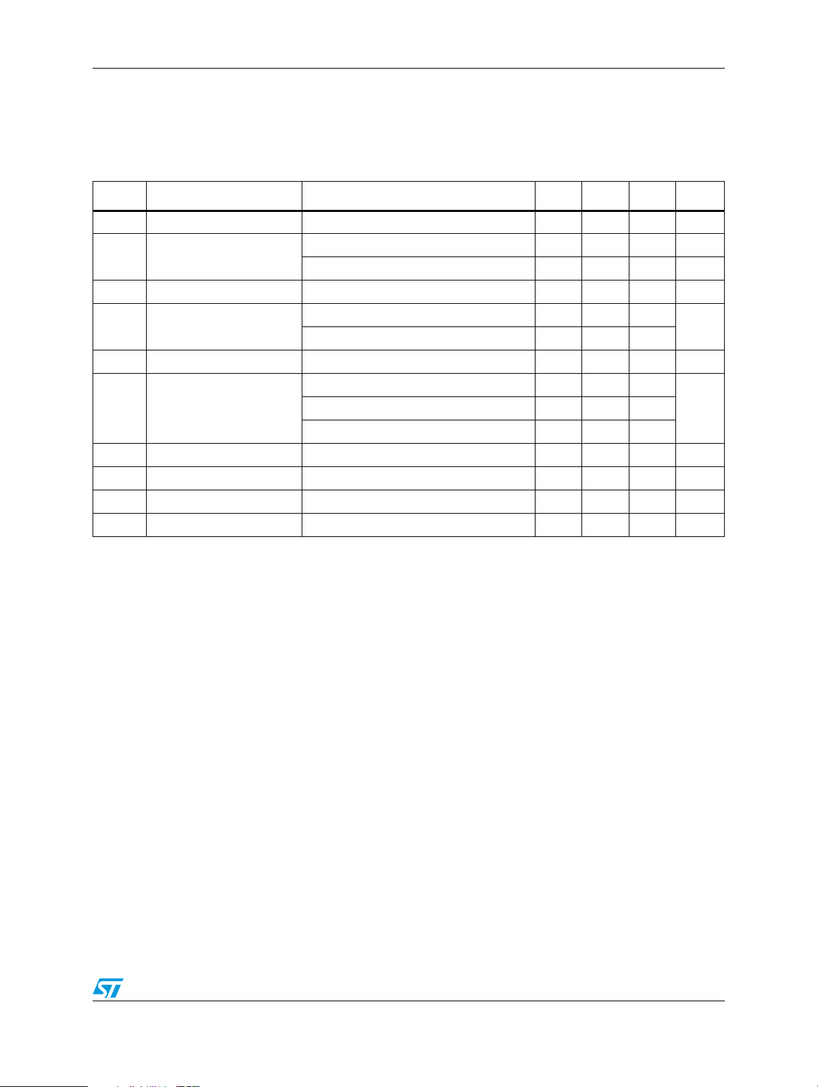
Table 5. Electrical characteristics (V
T
= -40 to 85°C, unless otherwise specified. Typical value are referred at TA = 25 °C)
A
= 2 to 3.6 V, C1 = C2 = 0.22 µF, C3 = C4 = 10 µF,
I
Symbol Parameter Test conditions Min. Typ. Max. Unit
V
Input voltage 2 3.6 V
I
V
= 2 to 3.6V, IO =0 to 20mA 4.8 5 5.2 V
V
Output voltage
O
V
RIPPLE
I
SHDN
Output voltage ripple No load, Full load 100 mV
I
No load supply current
i
Shutdown supply current VI = 2 to 3.6V, No Load, V
ν Efficiency
f
Switching frequency Full load 500 kHz
OSC
V
SHDN input threshold 0.7V
IH
SHDN input threshold 0.4 V
V
IL
SHDN input current V
I
IH
I
V
= 3 to 3.6V, IO=0 to 30mA 4.8 5 5.2 V
I
V
= 2 to 3V, No load 200 300
I
= 3 to 3.6V, No load 75 150
V
I
= V
SHDN
= 3V, IO =20mA 82
V
I
= 3V, IO =30mA 82
I
= 2V, IO =20mA 80
V
I
= V
SHDN
I
I
0.02 1 µA
I
0.005 ± 1µA
µA
%V
V
Note: Do not overload or short the output to ground. If the above conditions are not observed the
device may be damaged.
7/16
Page 8
Typical performance characteristics ST619LB
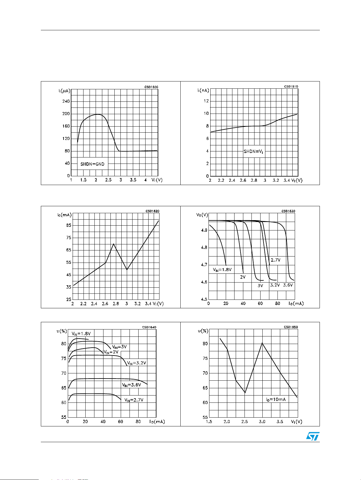
6 Typical performance characteristics
Figure 3. No load supply current vs input
voltage
Figure 5. Maximum output current vs input
voltage
Figure 4. Shutdown supply current vs input
voltage
Figure 6. Output voltage vs output current
Figure 7. Efficiency vs output current Figure 8. Efficiency vs input voltage
8/16
Page 9
ST619LB Typical performance characteristics
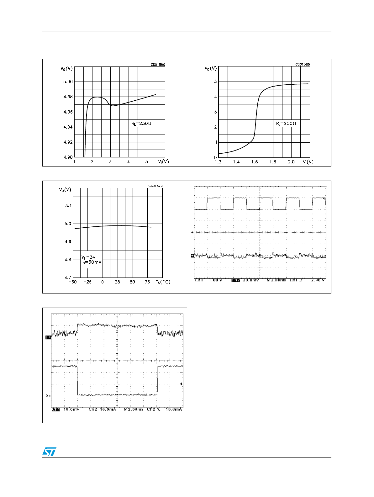
Figure 9. Output voltage vs input voltage Figure 10. Start-up
Figure 11. Output voltage vs temperature Figure 12. Line transient response
Figure 13. Load transient response
VI = 3 V, IO = 0 to 25 mA
RL = 250 Ω
9/16
Page 10
Application information ST619LB
7 Application information
7.1 Charge pump capacitors C1 and C2
The values of charge pump capacitors C1 and C2 are critical to ensure adequate output
current and avoid excessive peak currents. It is suggested to use values in the range of 0.22
µF to 1.0 µF and avoid the use of higher values of C
performance. Ceramic or tantalum capacitors are recommended.
7.2 Input and output capacitors C3 and C4
The type of input capacitor (C3) and output filter capacitor (C4) used is not critical, but it
does affect performance. Tantalum, ceramics or aluminium electrolytic are suggested. For
lowest ripple, use large, low effective series resistance (ESR) ceramic tantalum capacitors.
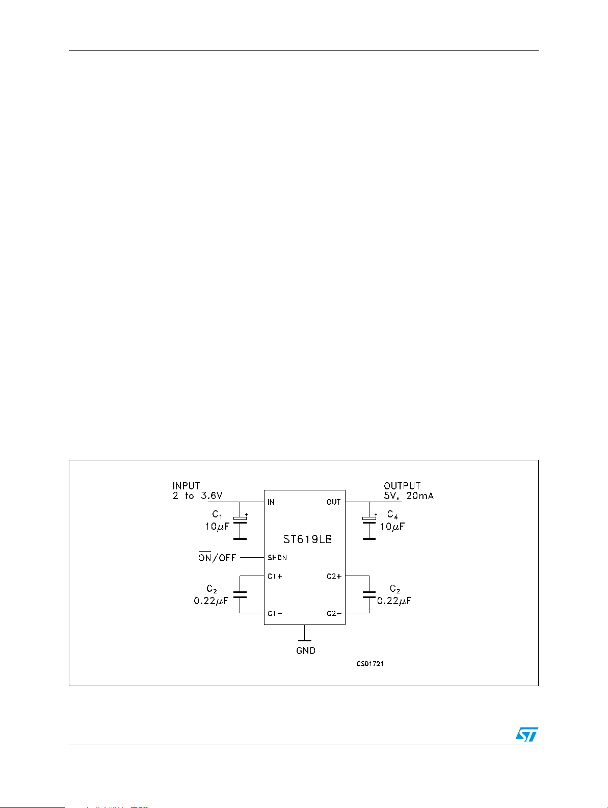
If the input supply source impedance is very low, C3 can be omitted. The typical application
circuit shows the component values for proper operation using minimal board space. The
input bypass capacitor (C3) and output filter capacitor (C4) should be at least 10 µF. Many
capacitors exhibit 40% to 50% variation over temperature. Compensate for capacitor
temperature coefficient by selecting a large nominal value to ensure proper operation over
temperature.
capacitors, in order to obtain best
O
7.3 Layout consideration
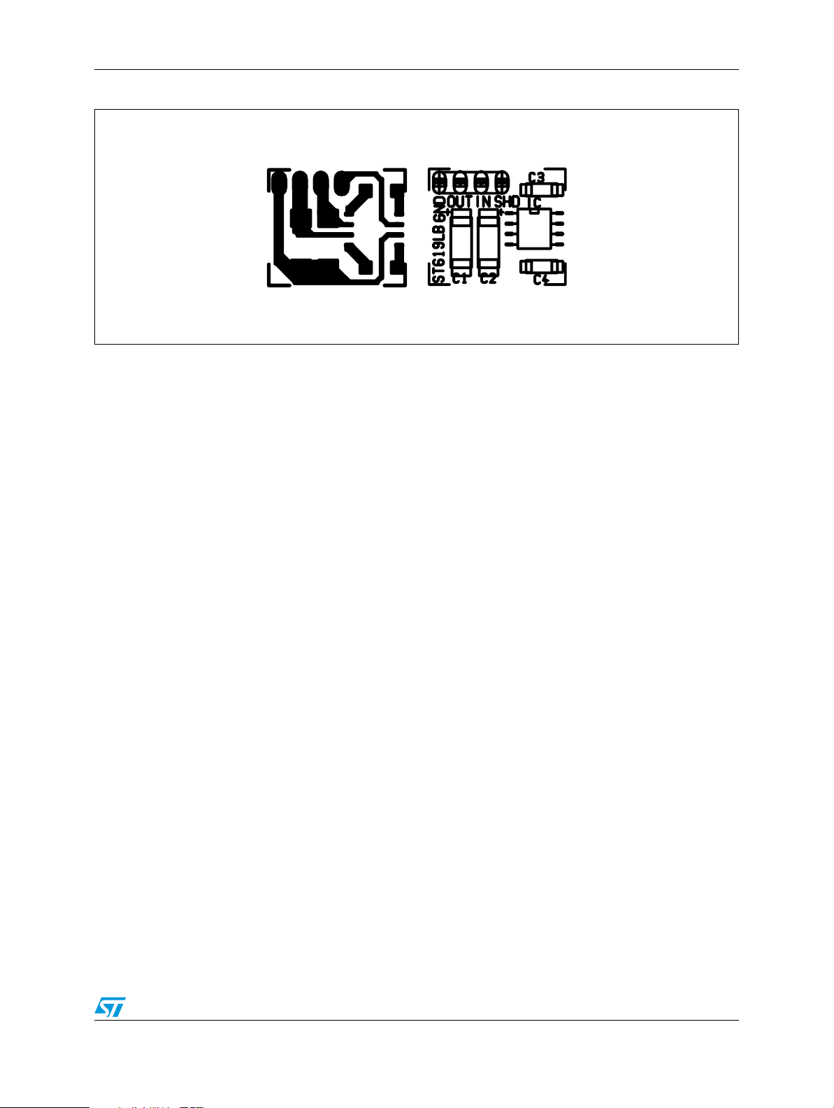
In the below figure, the typical application evaluation board of ST619LB is reported. A good
layout ensures stability and helps maintain the output voltage under heavy loads. For best
performance, use very short connections to the capacitors.
Figure 14. Typical application circuit
10/16
Page 11
ST619LB Application information
Figure 15. Typical application evaluation board
11/16
Page 12

Package mechanical data ST619LB
8 Package mechanical data
In order to meet environmental requirements, ST offers these devices in ECOPACK®
packages. These packages have a Lead-free second level interconnect. The category of
second Level Interconnect is marked on the package and on the inner box label, in
compliance with JEDEC Standard JESD97. The maximum ratings related to soldering
conditions are also marked on the inner box label. ECOPACK is an ST trademark.
ECOPACK specifications are available at: www.st.com.
12/16
Page 13
ST619LB Package mechanical data
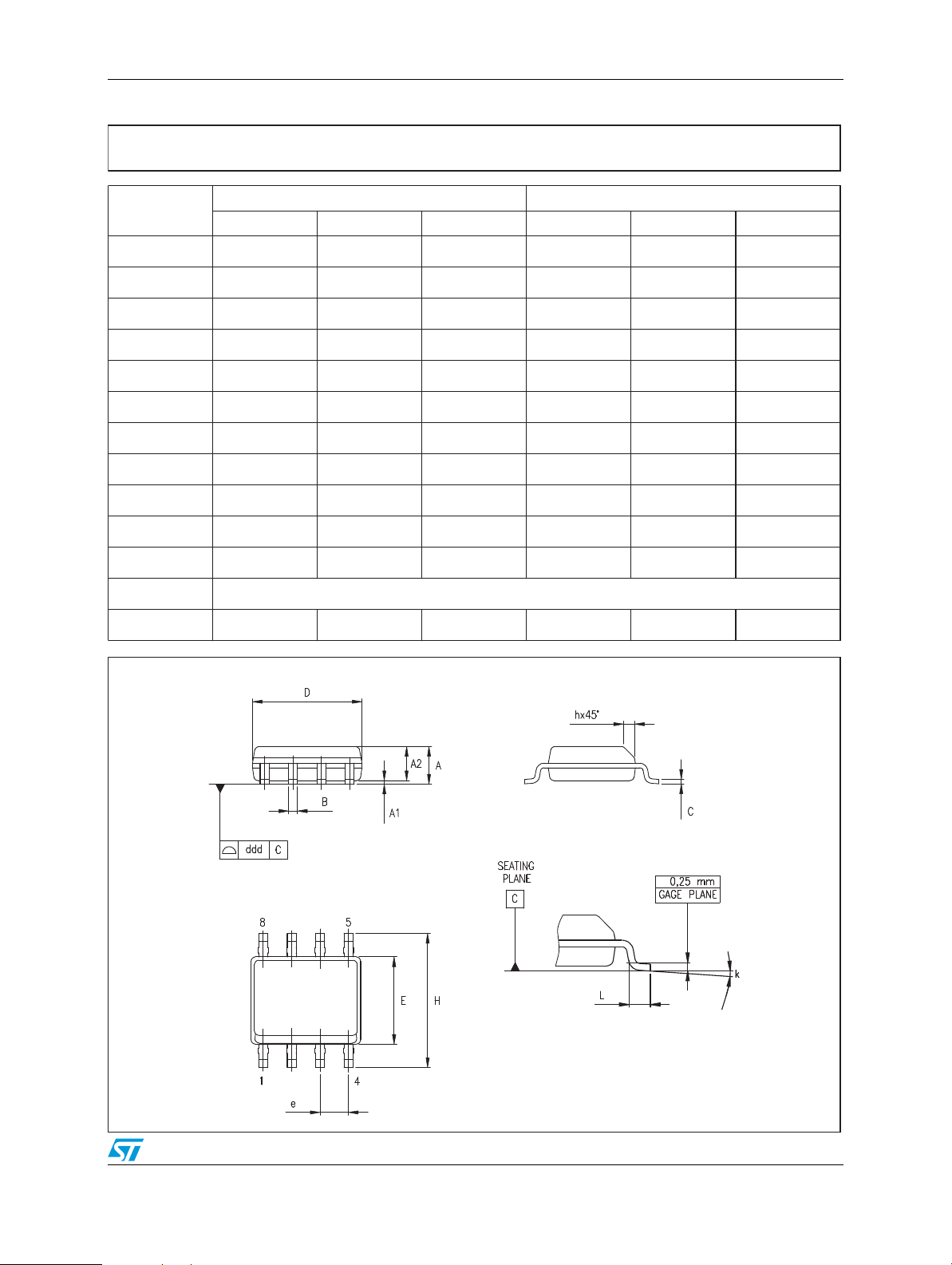
SO-8 mechanical data
Dim.
A1.35 1.75 0.053 0.069
A1 0.10 0.25 0.04 0.010
A2 1.10 1.65 0.043 0.065
B0.33 0.51 0.013 0.020
C0.19 0.25 0.007 0.010
D4.80 5.00 0.189 0.197
E 3.80 4.00 0.150 0.157
e 1.27 0.050
H5.80 6.20 0.228 0.244
h 0.25 0.50 0.010 0.020
L 0.40 1.27 0.016 0.050
k 8° (max.)
ddd 0.1 0.04
Min. Typ. Max. Min. Typ. Max.
mm. inch.
0016023/C
13/16
Page 14
Package mechanical data ST619LB
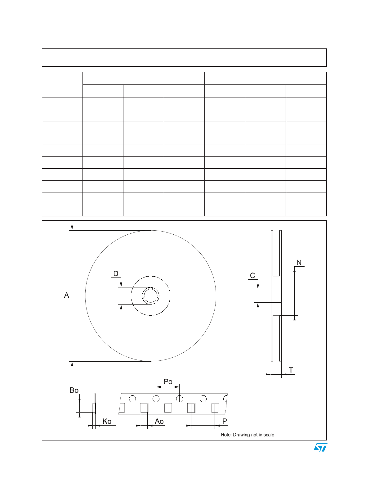
Tape & reel SO-8 mechanical data
mm. inch.
Dim.
Min. Typ. Max. Min. Typ. Max.
A 330 12.992
C 12.8 13.2 0.504 0.519
D 20.2 0.795
N60 2.362
T 22.4 0.882
Ao 8.1 8.5 0.319 0.335
Bo 5.5 5.9 0.216 0.232
Ko 2.1 2.3 0.082 0.090
Po 3.9 4.1 0.153 0.161
P7.98.1 0.311 0.319
14/16
Page 15
ST619LB Revision history
9 Revision history
Table 6. Document revision history
Date Revision Changes
21-Jun-2004 3
07-Nov-2007 4 Added Table 1.
15/16
Page 16

ST619LB
Please Read Carefully:
Information in this document is provided solely in connection with ST products. STMicroelectronics NV and its subsidiaries (“ST”) reserve the
right to make changes, corrections, modifications or improvements, to this document, and the products and services described herein at any
time, without notice.
All ST products are sold pursuant to ST’s terms and conditions of sale.
Purchasers are solely responsible for the choice, selection and use of the ST products and services described herein, and ST assumes no
liability whatsoever relating to the choice, selection or use of the ST products and services described herein.
No license, express or implied, by estoppel or otherwise, to any intellectual property rights is granted under this document. If any part of this
document refers to any third party products or services it shall not be deemed a license grant by ST for the use of such third party products
or services, or any intellectual property contained therein or considered as a warranty covering the use in any manner whatsoever of such
third party products or services or any intellectual property contained therein.
UNLESS OTHERWISE SET FORTH IN ST’S TERMS AND CONDITIONS OF SALE ST DISCLAIMS ANY EXPRESS OR IMPLIED
WARRANTY WITH RESPECT TO THE USE AND/OR SALE OF ST PRODUCTS INCLUDING WITHOUT LIMITATION IMPLIED
WARRANTIES OF MERCHANTABILITY, FITNESS FOR A PARTICULAR PURPOSE (AND THEIR EQUIVALENTS UNDER THE LAWS
OF ANY JURISDICTION), OR INFRINGEMENT OF ANY PATENT, COPYRIGHT OR OTHER INTELLECTUAL PROPERTY RIGHT.
UNLESS EXPRESSLY APPROVED IN WRITING BY AN AUTHORIZED ST REPRESENTATIVE, ST PRODUCTS ARE NOT
RECOMMENDED, AUTHORIZED OR WARRANTED FOR USE IN MILITARY, AIR CRAFT, SPACE, LIFE SAVING, OR LIFE SUSTAINING
APPLICATIONS, NOR IN PRODUCTS OR SYSTEMS WHERE FAILURE OR MALFUNCTION MAY RESULT IN PERSONAL INJURY,
DEATH, OR SEVERE PROPERTY OR ENVIRONMENTAL DAMAGE. ST PRODUCTS WHICH ARE NOT SPECIFIED AS "AUTOMOTIVE
GRADE" MAY ONLY BE USED IN AUTOMOTIVE APPLICATIONS AT USER’S OWN RISK.
Resale of ST products with provisions different from the statements and/or technical features set forth in this document shall immediately void
any warranty granted by ST for the ST product or service described herein and shall not create or extend in any manner whatsoever, any
liability of ST.
ST and the ST logo are trademarks or registered trademarks of ST in various countries.
Information in this document supersedes and replaces all information previously supplied.
The ST logo is a registered trademark of STMicroelectronics. All other names are the property of their respective owners.
© 2007 STMicroelectronics - All rights reserved
STMicroelectronics group of companies
Australia - Belgium - Brazil - Canada - China - Czech Republic - Finland - France - Germany - Hong Kong - India - Israel - Italy - Japan -
Malaysia - Malta - Morocco - Singapore - Spain - Sweden - Switzerland - United Kingdom - United States of America
www.st.com
16/16
 Loading...