

Page 1
2-bit dual supply bus transceiver level translator
Features
■ High speed:
–t
= 6.2 ns (max) at TA = 85 °C
PD
–V
–V
■ Low power dissipation:
–I
■ Symmetrical output impedance:
–|I
–|I
■ Balanced propagation delays:
–T
■
Power-down protection on inputs and outputs
■ 26 Ω series resistor on A side
■ Operating voltage range:
–V
–V
■ Max data rates:
– 380 Mbps (1.8 V to 3.3 V translation)
– 260 Mbps (<1.8 V to 3.3 V translation)
– 260 Mbps (translate to 2.5 V)
– 210 Mbps (translate to 1.5 V)
■ Latch-up performance exceeds 500 mA
(JESD17)
■ ESD performance:
– HBM > 2 kV (MIL STD 883 method 3015)
– MM > 200 V
= 1.8 V
CCB
= 3.3 V
CCA
= I
CCA
| = I
OHA
V
CCB
| = I
OHB
or 3.0 V; V
≈ T
PLH
CCA
CCB
= 5 µA (max) at TA = 85 °C
CCB
= 7 mA min at V
OLA
= 1.65 V or 2.3 V
= 2 mA min at V
OLB
= 1.65 V
CCB
PHL
(OPR) = 1.4 V to 3.6 V
(OPR) = 1.4 V to 3.6 V
= 2.75 V;
CCA
= 2.3 V
CCA
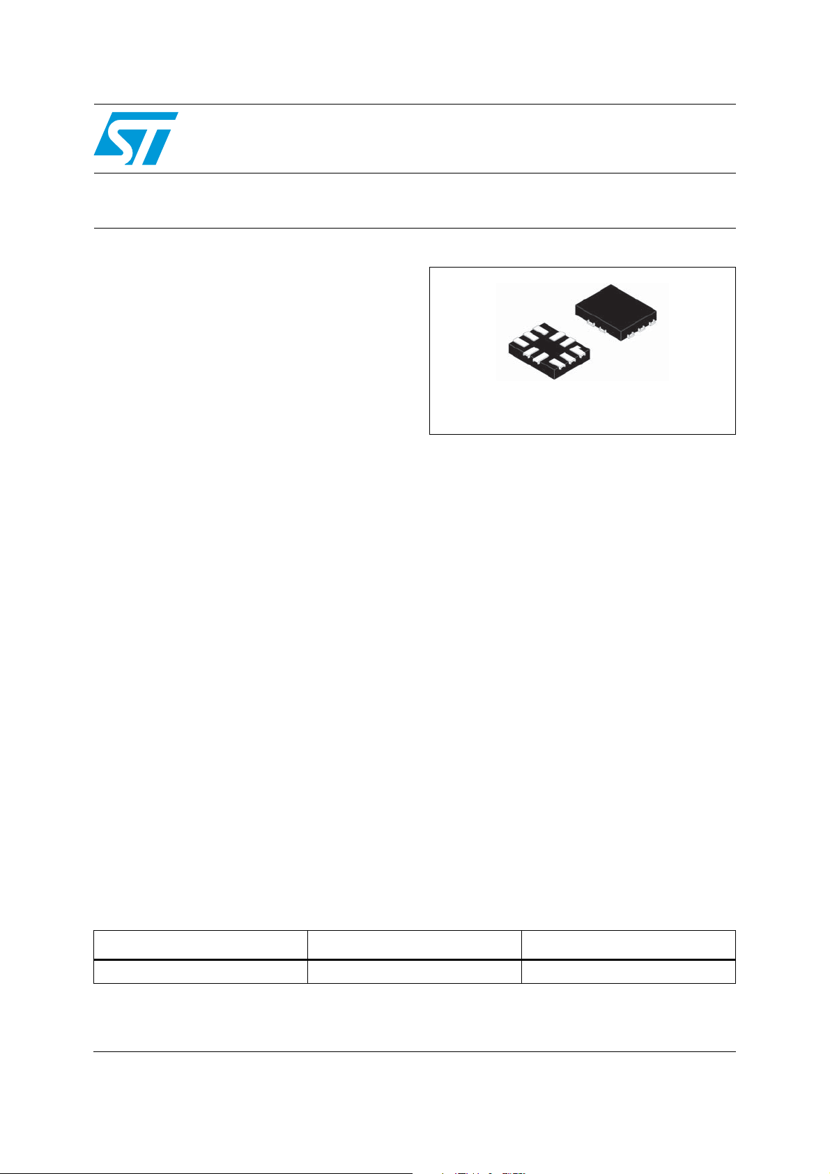
ST2G3236
with side series resistor
QFN10 (1.8 mm x 1.4 mm)
Description
The ST2G3236 is a dual supply, low-voltage
CMOS 2-bit bus transceiver produced with submicron silicon gate and five-layer metal wiring
2
C
MOS technology. Designed for use as an
interface between a 3.3 V bus and a 2.5 V or
1.8 V bus in mixed 3.3 V/1.8 V, 3.3 V/2.5 V and
2.5 V/1.8 V supply systems, it achieves high
speed operation while maintaining the CMOS low
power dissipation.
This IC is intended for two-way asynchronous
communication between data buses, and the
direction of data transmission is determined by
DIR inputs. The A-port interfaces with the 3 V bus,
and the B-port with the 2.5 V and 1.8 V bus.
All inputs are equipped with protection circuits to
protect against static discharge, giving them 2 kV
of ESD immunity and transient excess voltage.
Table 1. Device summary
Part number Package Packaging
ST2G3236 QFN10 (1.8 mm x 1.4 mm) Tape and reel
July 2010 Doc ID 12942 Rev 4 1/22
www.st.com
1
Page 2

Contents ST2G3236
Contents
1 Logic diagram and I/O equivalent circuit . . . . . . . . . . . . . . . . . . . . . . . . 5
1.1 Truth table . . . . . . . . . . . . . . . . . . . . . . . . . . . . . . . . . . . . . . . . . . . . . . . . . . 6
1.2 Application notes and recommendations . . . . . . . . . . . . . . . . . . . . . . . . . . 6
1.3 Recommended power-up sequence . . . . . . . . . . . . . . . . . . . . . . . . . . . . . 6
1.4 Recommended power-down sequence . . . . . . . . . . . . . . . . . . . . . . . . . . . 6
2 Pin connections and descriptions . . . . . . . . . . . . . . . . . . . . . . . . . . . . . . 7
2.1 Pin connections . . . . . . . . . . . . . . . . . . . . . . . . . . . . . . . . . . . . . . . . . . . . . 7
2.2 Pin descriptions . . . . . . . . . . . . . . . . . . . . . . . . . . . . . . . . . . . . . . . . . . . . . 7
3 Electrical ratings . . . . . . . . . . . . . . . . . . . . . . . . . . . . . . . . . . . . . . . . . . . . 8
4 Electrical characteristics . . . . . . . . . . . . . . . . . . . . . . . . . . . . . . . . . . . . . 9
4.1 DC electrical characteristics for V
4.2 DC electrical characteristics for V
4.3 AC electrical characteristics . . . . . . . . . . . . . . . . . . . . . . . . . . . . . . . . . . . 12
4.4 Capacitance characteristics . . . . . . . . . . . . . . . . . . . . . . . . . . . . . . . . . . . 13
. . . . . . . . . . . . . . . . . . . . . . . . . . . . 9
CCA
. . . . . . . . . . . . . . . . . . . . . . . . . . . 10
CCB
5 Test circuit . . . . . . . . . . . . . . . . . . . . . . . . . . . . . . . . . . . . . . . . . . . . . . . . 14
6 Waveforms . . . . . . . . . . . . . . . . . . . . . . . . . . . . . . . . . . . . . . . . . . . . . . . . 15
7 Package mechanical data . . . . . . . . . . . . . . . . . . . . . . . . . . . . . . . . . . . . 16
8 Revision history . . . . . . . . . . . . . . . . . . . . . . . . . . . . . . . . . . . . . . . . . . . 21
2/22 Doc ID 12942 Rev 4
Page 3

ST2G3236 List of tables
List of tables
Table 1. Device summary . . . . . . . . . . . . . . . . . . . . . . . . . . . . . . . . . . . . . . . . . . . . . . . . . . . . . . . . . . 1
Table 2. Truth table. . . . . . . . . . . . . . . . . . . . . . . . . . . . . . . . . . . . . . . . . . . . . . . . . . . . . . . . . . . . . . . 6
Table 3. Pin descriptions . . . . . . . . . . . . . . . . . . . . . . . . . . . . . . . . . . . . . . . . . . . . . . . . . . . . . . . . . . 7
Table 4. Absolute maximum ratings . . . . . . . . . . . . . . . . . . . . . . . . . . . . . . . . . . . . . . . . . . . . . . . . . . 8
Table 5. Recommended operating conditions . . . . . . . . . . . . . . . . . . . . . . . . . . . . . . . . . . . . . . . . . . 8
Table 6. DC specification for V
Table 7. DC specification for V
Table 8. AC electrical characteristics . . . . . . . . . . . . . . . . . . . . . . . . . . . . . . . . . . . . . . . . . . . . . . . . 12
Table 9. Capacitance characteristics . . . . . . . . . . . . . . . . . . . . . . . . . . . . . . . . . . . . . . . . . . . . . . . . 13
Table 10. Test values . . . . . . . . . . . . . . . . . . . . . . . . . . . . . . . . . . . . . . . . . . . . . . . . . . . . . . . . . . . . . 14
Table 11. Waveform symbol value . . . . . . . . . . . . . . . . . . . . . . . . . . . . . . . . . . . . . . . . . . . . . . . . . . . 15
Table 12. QFN10L (1.8 mm x 1.4 mm) mechanical data . . . . . . . . . . . . . . . . . . . . . . . . . . . . . . . . . . 17
Table 13. Revision history . . . . . . . . . . . . . . . . . . . . . . . . . . . . . . . . . . . . . . . . . . . . . . . . . . . . . . . . . 21
. . . . . . . . . . . . . . . . . . . . . . . . . . . . . . . . . . . . . . . . . . . . . . . . . . . 9
CCA
CCB . . . . . . . . . . . . . . . . . . . . . . . . . . . . . . . . . . . . . . . . . . . . . . . . . . . . . . . . . . . . . . .10
Doc ID 12942 Rev 4 3/22
Page 4

List of figures ST2G3236
List of figures
Figure 1. Logic diagram . . . . . . . . . . . . . . . . . . . . . . . . . . . . . . . . . . . . . . . . . . . . . . . . . . . . . . . . . . . . 5
Figure 2. I/O equivalent circuit . . . . . . . . . . . . . . . . . . . . . . . . . . . . . . . . . . . . . . . . . . . . . . . . . . . . . . 5
Figure 3. Pin connections (top through view). . . . . . . . . . . . . . . . . . . . . . . . . . . . . . . . . . . . . . . . . . . . 7
Figure 4. Test circuit . . . . . . . . . . . . . . . . . . . . . . . . . . . . . . . . . . . . . . . . . . . . . . . . . . . . . . . . . . . . . 14
Figure 5. Waveform - propagation delay (f = 1 MHz, 50% duty cycle). . . . . . . . . . . . . . . . . . . . . . . . 15
Figure 6. Waveform - output enable and disable time (f = 1 MHz, 50% duty cycle) . . . . . . . . . . . . . 15
Figure 7. QFN10L (1.8 mm x 1.4 mm) package mechanical outline . . . . . . . . . . . . . . . . . . . . . . . . . 17
Figure 8. QFN10L (1.8 mm x 1.4 mm) footprint recommendation . . . . . . . . . . . . . . . . . . . . . . . . . . . 18
Figure 9. QFN10L (1.8 mm x 1.4 mm) carrier tape . . . . . . . . . . . . . . . . . . . . . . . . . . . . . . . . . . . . . . 18
Figure 10. QFN10L (1.8 mm x 1.4 mm) reel information - back view . . . . . . . . . . . . . . . . . . . . . . . . . 19
Figure 11. QFN10L (1.8 mm x 1.4 mm) reel information - front view. . . . . . . . . . . . . . . . . . . . . . . . . . 20
4/22 Doc ID 12942 Rev 4
Page 5

ST2G3236 Logic diagram and I/O equivalent circuit
1 Logic diagram and I/O equivalent circuit
Figure 1. Logic diagram
1B1A
DIR1
DIR2
A2
Figure 2. I/O equivalent circuit
OE
OE
B2
AM04932v1
CS15740
Doc ID 12942 Rev 4 5/22
Page 6

Logic diagram and I/O equivalent circuit ST2G3236
1.1 Truth table
Table 2. Truth table
Inputs Function
Output
OE
L L Output Input B => A
L H Input Output B <= A
H X High-Z High-Z HIGH-Z
DIRn A BUS B BUS
1.2 Application notes and recommendations
1. Once the device is enabled (OE = low), even if the input is floating, output may be either
on high or low logic level only, not in a high-impedance state. Output is in a highimpedance state only when OE
2. Unused I/O channel should be connected to GND or to the corresponding supply.
3. The OE
to V
V
and DIRn block is powered by V
. The OE and DIRn input high level can be equal to or greater than V
CCB
max.
IHB
4. Any input high level can be higher than the corresponding input supply voltage, up to
V
IHA
max (V
IHB
max).
Example:
= high.
and these input logic levels are referenced
CCB
CCB
, up to
V
= 1.8 V, V
CCA
= 2.6 V, OE = Low, DIRn = Low (B → A direction)
CCB
==> if I/O Bn = 3 V, I/O An = 1.8 V
5. If V
CCA
= V
= 0 V and OE = 0 V, An and Bn are isolated even if there is a signal on
CCB
An or Bn.
6. If the ST2G3236QTR is used in a UART application, there is a possibility of floating
input condition if the cable is disconnected, therefore a pull-down resistor is
recommended on the input port.
1.3 Recommended power-up sequence
1. Apply power to either VCC.
2. Apply power to the OE
input and to the respective data inputs. This may occur at the
same time as step 1.
3. Apply power to the other V
4. Drive the OE
input LOW to enable the device.
CC
.
1.4 Recommended power-down sequence
1. Drive the OE input HIGH to disable the device.
2. Remove power from either V
3. Remove power from the other V
CC
.
CC
.
6/22 Doc ID 12942 Rev 4
Page 7
ST2G3236 Pin connections and descriptions
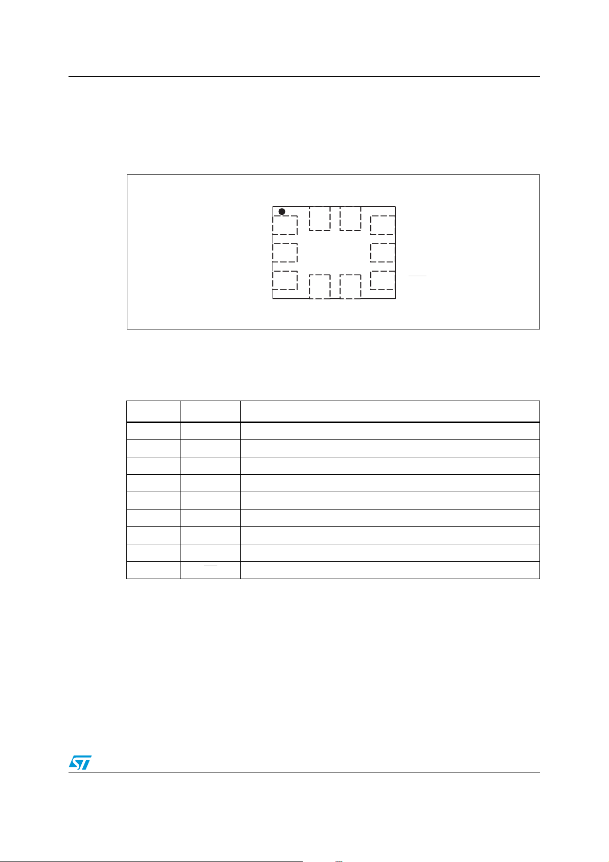
2 Pin connections and descriptions
2.1 Pin connections
Figure 3. Pin connections (top through view)
A2
A1
10
9
1
8
V
CCA
2.2 Pin descriptions
Table 3. Pin descriptions
Pin Symbol Name and function
1, 3 DIR1, DIR2 Directional controls
10 A1 Data inputs/outputs
4 B1 Data outputs/inputs
9 A2 Data inputs/outputs
5 B2 Data outputs/inputs
7 GND Ground (0 V)
8V
2V
6OE
CCA
CCB
CCB
2
3
4
V
B1
Positive supply voltage
Positive supply voltage
Output enable (active low)
5
B2
7
GND
OE
6
OE
AM04933v1
Doc ID 12942 Rev 4 7/22
Page 8

Electrical ratings ST2G3236
3 Electrical ratings
Stressing the device above the rating listed in the absolute maximum ratings table may
cause permanent damage to the device. These are stress ratings only and operation of the
device at these or any other conditions above those indicated in the operating sections of
this specification is not implied. Exposure to absolute maximum rating conditions for
extended periods may affect device reliability.
Table 4. Absolute maximum ratings
Symbol Parameter Value Unit
V
CCA
V
CCB
V
V
I/OA
V
I/OB
V
I/OA
V
I/OB
I
IK
I
OK
I
OA
I
OB
I
CCA
I
CCB
P
D
T
stg
T
L
Table 5. Recommended operating conditions
Supply voltage -0.5 to 4.6 V
Supply voltage -0.5 to 4.6 V
DC input voltage -0.5 to 4.6 V
I
DC I/O voltage (output disabled) -0.5 to 4.6 V
DC I/O voltage (output disabled) -0.5 to 4.6 V
DC output voltage -0.5 to V
DC output voltage -0.5 to V
CCA
CCB
DC input diode current -20 mA
DC output diode current -50 mA
DC output current ±50 mA
DC output current ±50 mA
DC VCC or ground current ±100 mA
DC VCC or ground current ±100 mA
Power dissipation 200 mW
Storage temperature -65 to +150 °C
Lead temperature (10 s) 260 °C
+ 0.5 V
+ 0.5 V
Symbol Parameter Value Unit
V
CCA
V
CCB
V
V
I/OA
V
I/OB
T
op
dt/dv Input rise and fall time
1. VIN from 0.8 V to 2.0 V at VCC = 3.0 V
Supply voltage 1.4 to 3.6 V
Supply voltage 1.4 to 3.6 V
Input voltage (DIRn, OE) 0 to V
I
I/O voltage 0 to V
I/O voltage 0 to V
Operating temperature -40 to +85 °C
V
= 3.0 to 3.6 V 0 to 10 ns/V
CCB
(1)
= 2.3 to 2.7 V 0 to 20 ns/V
V
CCB
V
= 1.4 to 1.95 V 0 to 100 ns/V
CCB
8/22 Doc ID 12942 Rev 4
CCB
CCA
CCB
V
V
V
Page 9

ST2G3236 Electrical characteristics
4 Electrical characteristics
4.1 DC electrical characteristics for V
Table 6. DC specification for V
Sym. Parameter
High level
input
V
IHA
voltage
(An)
Low level
input
V
ILA
voltage
(An)
High level
V
OHA
output
voltage
Low level
V
OLA
output
voltage
Input
I
leakage
IA
current
High
impedance
I
output
OZA
leakage
current
(1)
V
CCB
(V)
1.4 to 3.3 V
1.4 to 3.3 V
1.4 to 3.3 V
1.4 to 3.3 V
2.7 3.3 VI = VCC or GND ±0.5 ±5
1.4 2.7 V
2.7 3.3
CCA
Test conditions Value
(1)
V
CCA
(V)
1.4 0.65V
1.8 0.65V
2.5 1.6 1.6
3.3 2.0 2.0
1.4 0.35V
1.8 0.35V
2.5 0.7 0.7
3.3 0.8 0.8
1.4 IO = -100 µA 1.2 1.2
2.75 I
2.75 I
2.3 I
1.65 I
1.4 I
1.4 I
2.75 I
2.75 I
2.3 I
1.65 I
1.4 I
= -0.4 mA 2.5 2.5
O
= -7 mA 2.2 2.2
O
= -5 mA 1.8 1.8
O
= -2 mA 1.4 1.4
O
= - 1mA 1.1 1.1
O
= 100 µA 0.20 0.20
O
= 1 mA 0.40 0.40
O
= 7 mA 0.55 0.55
O
= 5 mA 0.40 0.40
O
= 2 mA 0.25 0.25
O
= 1 mA 0.20 0.20
O
= 3.6V or GND ±0.5 ±5
I
VIA= GND or 3.6 V
= V
IHB
OE = V
or V
CCB
ILB
V
IB
CCA
= 25 °C -40 to 85 °C
T
A
Min Max Min Max
CCA
CCA
0.65V
0.65V
CCA
CCA
3.6 V
0.35V
0.35V
CCA
CCA
3.6
±1.0 ±10 μA
CCA
CCA
Unit
V
V
V
μA
Doc ID 12942 Rev 4 9/22
Page 10

Electrical characteristics ST2G3236
Table 6. DC specification for V
(continued)
CCA
Test conditions Value
Sym. Parameter
Power
OFF
I
OFF
leakage
current
Quiescent
I
supply
CCtA
current
Maximum
quiescent
ΔI
CCtA
supply
current /
input (An)
1. VCC range = 3.3 ± 0.3; 2.5 ± 0.2 V; 1.8 ± 0.15 V
V
CCB
(V)
(1)
V
CCA
(V)
(1)
00
1.95 2.7
2.7 3.3
1.95 2.7
1.95 3.3
2.7 3.3
=GND to 3.6 V
V
IA
=GND to 3.6 V
V
IB
, DIR=GND to
OE
3.6 V
V
IA=VCCA
V
IB=VCCB
V
IA=VCCA
V
IB=VCCB
or GND
or GND
-0.6 V
or GND
4.2 DC electrical characteristics for V
= 25 °C -40 to 85 °C
T
A
Min Max Min Max
±1.0 ±10 μA
0.5 5 μA1.95 3.3
0.75 mA
CCB
Unit
Table 7. DC specification for V
Test conditions Value
Sym. Parameter
High level
input
V
voltage
IHB
(Bn, DIRn,
)
OE
Low level
input
V
voltage
ILB
(Bn, DIRn,
)
OE
(1)
V
CCB
(V)
V
CCA
(V)
1.4
1.8 0.65V
2.5 1.6 1.6
1.4 to
3.3 V
3.3 2.0 2.0
1.4
1.8 0.35V
2.5 0.7 0.7
1.4 to
3.3 V
3.3 0.8 0.8
CCB
(1)
CCB
CCB
Unit
V
TA = 25°C -40 to 85°C
Min Max Min Max
CCB
CCB
0.65V
0.65V
CCB
CCB
0.65V
CCB
CCB
3.6
0.35V
3.6 V
0.35V
0.35V
10/22 Doc ID 12942 Rev 4
Page 11

ST2G3236 Electrical characteristics
Table 7. DC specification for V
CCB
Test conditions Value
Sym. Parameter
V
CCB
(V)
(1)
V
CCA
(V)
(1)
1.4
1.8 I
2.75 I
2.75 I
1.4 to
3.3 V
2.3 I
V
OHB
High level
output
voltage
1.65 I
1.4 I
1.4
1.8 I
2.75 I
2.75 I
1.4 to
3.3 V
2.3 I
V
OLB
Low level
output
voltage
1.65 I
1.4 I
I
IB
Input
leakage
current
2.7 3.3 VI = VCC or GND ±0.5 ±5
1.4 2.7 V
High
impedance
I
OZB
output
2.7 3.3
leakage
current
Quiescent
I
CCtB
supply
current
Maximum
quiescent
CCtB
supply
current /
ΔI
input (Bn,
DIRn, OE
1. VCC range = 3.3 ± 0.3; 2.5 ± 0.2 V; 1.8 ± 0.15 V
1.95 2.7
2.7 3.3
1.95 2.7
1.95 3.3
2.7 3.3
)
(continued)
= 25°C -40 to 85°C
T
A
Min Max Min Max
= -100 µA 1.3 1.3
I
O
= -100 µA 1.6 1.6
O
= -20 mA 2.2 2.2
O
= -15 mA 1.7 1.7
O
= -4 mA 1.44 1.44
O
= -2 mA 1.5 1.5
O
= -2 mA 1.25 1.25
O
I
= 100 µA 0.1 0.1
O
= 100 µA 0.2 0.2
O
= 20 mA 0.55 0.55
O
= 15 mA 0.35 0.35
O
= 4 mA 0.39 0.39
O
= 2 mA 0.20 0.20
O
= 2 mA 0.15 0.15
O
= 3.6 V or GND ±0.5 ±5
I
V
= V
IA
V
IB
V
IA=VCCA
V
IB=VCCB
VIB=V
V
IA=VCCA
or V
IHA
ILA
= GND or 3.6 V
=V
OE
CCB
or GND
or GND
- 0.6 V
CCB
or GND
±1.0 ±10 μA
0.5 5 μA1.95 3.3
Unit
V
V
μA
0.75 mA
Doc ID 12942 Rev 4 11/22
Page 12

Electrical characteristics ST2G3236
4.3 AC electrical characteristics
Table 8. AC electrical characteristics
Test condition Value
Symbol Parameter
V
CCB
(V) V
CCA
(V)
-40 to 85 °C
Min Max
t
PLH tPHL
Propagation delay time
An to Bn
1.8 ± 0.15 2.5 ± 0.2
= 30 pF
C
L
= 500 Ω
R
L
1.0 5.8
2.5 ± 0.2 3.3 ± 0.3 1.0 4.4
t
PLH tPHL
Propagation delay time
Bn to An
1.8 ± 0.15 2.5 ± 0.2
= 30 pF
C
L
= 500 Ω
R
L
1.0 5.5
2.5 ± 0.2 3.3 ± 0.3 1.0 4.0
t
PZL tPZH
Output enable time OE
to An
1.8 ± 0.15 2.5 ± 0.2
= 30 pF
C
L
= 500 Ω
R
L
1.0 5.4
2.5 ± 0.2 3.3 ± 0.3 1.0 4.0
t
PZL tPZH
Output enable time OE
to Bn
1.8 ± 0.15 2.5 ± 0.2
= 30 pF
C
L
= 500 Ω
R
L
1.0 5.3
2.5 ± 0.2 3.3 ± 0.3 1.0 4.6
t
PLZ tPHZ
Output disable time
OE to An
1.8 ± 0.15 2.5 ± 0.2
= 30 pF
C
L
= 500 Ω
R
L
1.0 5.2
2.5 ± 0.2 3.3 ± 0.3 1.0 4.8
t
PLZ tPHZ
Output disable time
to Bn
OE
1.8 ± 0.15 2.5 ± 0.2
= 30 pF
C
L
= 500 Ω
R
L
1.0 4.6
2.5 ± 0.2 3.3 ± 0.3 1.0 4.4
t
OSLH
t
OSHL
Output to output skew
(1) (2)
time
1.8 ± 0.15 2.5 ± 0.2
= 30 pF
C
L
= 500 Ω
R
L
0.5
2.5 ± 0.2 3.3 ± 0.3 0.75
1. Skew is defined as the absolute value of the difference between the actual propagation delay for any two outputs of the
same device switching in the same direction, either HIGH or LOW (Toslh = | t
2. Parameter guaranteed by design
PLHm
– t
PLHn
|, t
OSHL
= | t
PHLm
- t
PHLn
|
Unit
ns1.8 ± 0.15 3.3 ± 0.3 1.0 6.2
ns1.8 ± 0.15 3.3 ± 0.3 1.0 5.1
ns1.8 ± 0.15 3.3 ± 0.3 1.0 5.1
ns1.8 ± 0.15 3.3 ± 0.3 1.0 5.2
ns1.8 ± 0.15 3.3 ± 0.3 1.0 5.6
ns1.8 ± 0.15 3.3 ± 0.3 1.0 4.5
ns1.8 ± 0.15 3.3 ± 0.3 0.5
12/22 Doc ID 12942 Rev 4
Page 13

ST2G3236 Electrical characteristics
4.4 Capacitance characteristics
Table 9. Capacitance characteristics
Test condition Value
Symbol Parameter
C
C
C
PD
1. CPD is defined as the value of the IC's internal equivalent capacitance, which is calculated from the
operating current consumption without load. (Refer to Figure 4: Test circuit). Average current can be
obtained by the following equation. ICC(opr) - CPD x VCC x fIN + ICC/16 (per circuit)
Input capacitance Open Open - 5 - - - pF
INB
Input/output
I/O
capacitance
Power dissipation
(1)
capacitance
V
V
CCB
(V)
CCA
(V)
2.5 3.3 - 6 - - - pF
2.5 3.3 f=10 MHz - 29 - - -
1.8 3.3 - 29 - - -
= 25 °C -40 to 85 °C
T
A
Min. Typ. Max. Min. Max.
Unit
pF
Doc ID 12942 Rev 4 13/22
Page 14

Test circuit ST2G3236
5 Test circuit
Figure 4. Test circuit
SC11690
Table 10. Test values
Tes t Sw itch
t
PLH
t
PZ
t
PZL
t
PZH
, t
PHL
L, t
(VCC = 3.0 to 3.6 V) 6 V
PLZ
, t
(VCC = 2.3 to 2.7 V or VCC = 1.6 to 1.95 V) 2V
PLZ
, t
PHZ
Open
CC
GND
14/22 Doc ID 12942 Rev 4
Page 15

ST2G3236 Waveforms
6 Waveforms
Table 11. Waveform symbol value
V
Symbol
V
IH
V
M
V
X
V
Y
3.0 to 3.6V 2.3 to 2.7V 1.65 to 1.95V
V
CC
1.5V VCC/2 VCC/2
V
+ 0.3V V
OL
V
- 0.3V V
OL
OL
CC
V
CC
+ 0.15V V
- 0.15V V
OL
V
OL
OL
CC
+ 0.15V
- 0.15V
● C
● R
● R
= 30 pF or equivalent (includes jig and probe capacitance)
L
= R1 = 500 Ω or equivalent
L
T
= Z
of pulse generator (typically 50 Ω)
OUT
Figure 5. Waveform - propagation delay (f = 1 MHz, 50% duty cycle)
CS05160
Figure 6. Waveform - output enable and disable time (f = 1 MHz, 50% duty cycle)
SC13231
Doc ID 12942 Rev 4 15/22
Page 16

Package mechanical data ST2G3236
7 Package mechanical data
In order to meet environmental requirements, ST offers these devices in different grades of
ECOPACK
specifications, grade definitions and product status are available at: www.st.com.
ECOPACK
®
packages, depending on their level of environmental compliance. ECOPACK®
®
is an ST trademark.
16/22 Doc ID 12942 Rev 4
Page 17

ST2G3236 Package mechanical data
Table 12. QFN10L (1.8 mm x 1.4 mm) mechanical data
ref.
Nom Min Max Nom Min Max
A 0.50 0.45 0.55 0.020 0.017 0.021
A1 0.02 0 0.05 0.001 0 0.002
A3 0.127 0.005 0 0
b 0.20 0.15 0.25 0.007 0.006 0.010
D 1.80 1.70 1.90 0.070 0.066 0.074
E 1.40 1.30 1.50 0.055 0.051 0.059
e 0.40 0.015
L 0.40 0.30 0.50 0.015 0.011 0.020
mm inch
Figure 7. QFN10L (1.8 mm x 1.4 mm) package mechanical outline
Doc ID 12942 Rev 4 17/22
Page 18

Package mechanical data ST2G3236
Figure 8. QFN10L (1.8 mm x 1.4 mm) footprint recommendation
Figure 9. QFN10L (1.8 mm x 1.4 mm) carrier tape
18/22 Doc ID 12942 Rev 4
Page 19

ST2G3236 Package mechanical data
Figure 10. QFN10L (1.8 mm x 1.4 mm) reel information - back view
Doc ID 12942 Rev 4 19/22
Page 20

Package mechanical data ST2G3236
Figure 11. QFN10L (1.8 mm x 1.4 mm) reel information - front view
20/22 Doc ID 12942 Rev 4
Page 21

ST2G3236 Revision history
8 Revision history
Table 13. Revision history
Date Revision Changes
06-Dec-2006 1 First release
31-Mar-2010 2
21-Apr-2010 3
23-Jul-2010 4
Corrected the value for V
conditions, from “0 to V
Table 5: Recommended operating
I in
” to “0 to V
CCA
CCB
”.
Minor formatting and text changes throughout the document.
Added footnote to Table 4: Absolute maximum ratings on
page 8.
Updated Figure 1, Section 3, Ta bl e 6 , 7; added Section 1.2;
reformatted document; minor textual changes.
Doc ID 12942 Rev 4 21/22
Page 22

ST2G3236
Please Read Carefully:
Information in this document is provided solely in connection with ST products. STMicroelectronics NV and its subsidiaries (“ST”) reserve the
right to make changes, corrections, modifications or improvements, to this document, and the products and services described herein at any
time, without notice.
All ST products are sold pursuant to ST’s terms and conditions of sale.
Purchasers are solely responsible for the choice, selection and use of the ST products and services described herein, and ST assumes no
liability whatsoever relating to the choice, selection or use of the ST products and services described herein.
No license, express or implied, by estoppel or otherwise, to any intellectual property rights is granted under this document. If any part of this
document refers to any third party products or services it shall not be deemed a license grant by ST for the use of such third party products
or services, or any intellectual property contained therein or considered as a warranty covering the use in any manner whatsoever of such
third party products or services or any intellectual property contained therein.
UNLESS OTHERWISE SET FORTH IN ST’S TERMS AND CONDITIONS OF SALE ST DISCLAIMS ANY EXPRESS OR IMPLIED
WARRANTY WITH RESPECT TO THE USE AND/OR SALE OF ST PRODUCTS INCLUDING WITHOUT LIMITATION IMPLIED
WARRANTIES OF MERCHANTABILITY, FITNESS FOR A PARTICULAR PURPOSE (AND THEIR EQUIVALENTS UNDER THE LAWS
OF ANY JURISDICTION), OR INFRINGEMENT OF ANY PATENT, COPYRIGHT OR OTHER INTELLECTUAL PROPERTY RIGHT.
UNLESS EXPRESSLY APPROVED IN WRITING BY AN AUTHORIZED ST REPRESENTATIVE, ST PRODUCTS ARE NOT
RECOMMENDED, AUTHORIZED OR WARRANTED FOR USE IN MILITARY, AIR CRAFT, SPACE, LIFE SAVING, OR LIFE SUSTAINING
APPLICATIONS, NOR IN PRODUCTS OR SYSTEMS WHERE FAILURE OR MALFUNCTION MAY RESULT IN PERSONAL INJURY,
DEATH, OR SEVERE PROPERTY OR ENVIRONMENTAL DAMAGE. ST PRODUCTS WHICH ARE NOT SPECIFIED AS "AUTOMOTIVE
GRADE" MAY ONLY BE USED IN AUTOMOTIVE APPLICATIONS AT USER’S OWN RISK.
Resale of ST products with provisions different from the statements and/or technical features set forth in this document shall immediately void
any warranty granted by ST for the ST product or service described herein and shall not create or extend in any manner whatsoever, any
liability of ST.
ST and the ST logo are trademarks or registered trademarks of ST in various countries.
Information in this document supersedes and replaces all information previously supplied.
The ST logo is a registered trademark of STMicroelectronics. All other names are the property of their respective owners.
© 2010 STMicroelectronics - All rights reserved
STMicroelectronics group of companies
Australia - Belgium - Brazil - Canada - China - Czech Republic - Finland - France - Germany - Hong Kong - India - Israel - Italy - Japan -
Malaysia - Malta - Morocco - Philippines - Singapore - Spain - Sweden - Switzerland - United Kingdom - United States of America
www.st.com
22/22 Doc ID 12942 Rev 4
 Loading...