

Page 1
Features
ST2L05-3300
Very low quiescent current dual voltage regulator
■ V
■ V
■
■ Guaranteed current of output 2: 1 A
■ ± 2% output tolerance (at 25 °C)
■ ± 3% output tolerance at overtemperature
■ Typical dropout 1.1 V (I
■ Internal power and thermal limit
■ Good stability with low ESR output capacitor
■ Operating temperature range: 0 °C to 125 °C
■ Very low quiescent current: 7 mA max
: fixed
O1
: adjustable from 1.25 to VI - V
O2
Guaranteed current of output 1: 1 A
= IO2 = 1 A)
O1
DROP
overtemperature
■ Available in DFN8 5x6 mm package
Applications
■ Hard disk drives
■ CD/DVD-ROMs
■ CD/DVD-R/RWs
■ COMBO
®
(DVD-ROM+CD-R/RW)
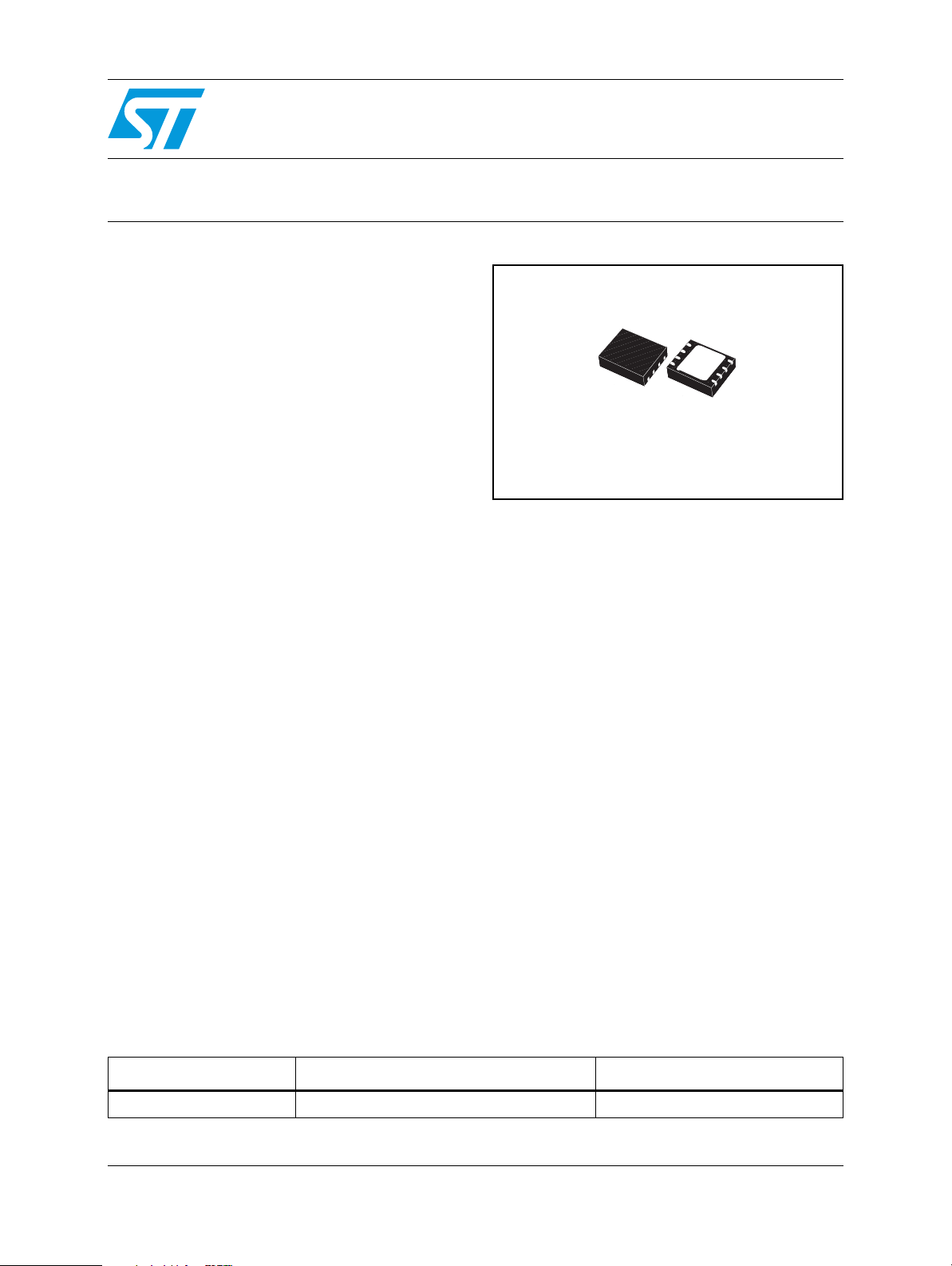
DFN8 (5x6 mm)
and overtemperature protected. Also noteworthy
is the very good thermal performance of the DFN
package, with only 2 °C/W of thermal resistance
junction-to-case.
Description
Specifically designed for data storage
applications, this device integrates two voltage
regulators, each capable of supplying 1 A of
current. It is assembled in an 8-pin DFN8 5x6 mm
surface mounting package. One regulator block
supplies 3.3 V and, on request, 1.5 V, 1.8 V, 2.5 V,
2.8 V and 3.0 V. The other is adjustable from 1.25
V to V
- V
I
several different types of microcontroller. Both
outputs are current-limited
Table 1. Device summary
Order code Package Output voltage
ST2L05R3300PS DFN8 (5x6 mm) Adjustable
February 2009 Rev 7 1/29
, which is suitable for powering
DROP
www.st.com
29
Page 2

Contents ST2L05-3300
Contents
1 Block diagram . . . . . . . . . . . . . . . . . . . . . . . . . . . . . . . . . . . . . . . . . . . . . . 3
2 Pin configuration . . . . . . . . . . . . . . . . . . . . . . . . . . . . . . . . . . . . . . . . . . . . 4
3 Maximum ratings . . . . . . . . . . . . . . . . . . . . . . . . . . . . . . . . . . . . . . . . . . . . 5
4 Application circuits . . . . . . . . . . . . . . . . . . . . . . . . . . . . . . . . . . . . . . . . . . 6
5 Electrical characteristics . . . . . . . . . . . . . . . . . . . . . . . . . . . . . . . . . . . . . 7
6 Application hints . . . . . . . . . . . . . . . . . . . . . . . . . . . . . . . . . . . . . . . . . . . 15
6.1 External capacitors . . . . . . . . . . . . . . . . . . . . . . . . . . . . . . . . . . . . . . . . . . 15
6.2 Input capacitor . . . . . . . . . . . . . . . . . . . . . . . . . . . . . . . . . . . . . . . . . . . . . 15
6.3 Output capacitor . . . . . . . . . . . . . . . . . . . . . . . . . . . . . . . . . . . . . . . . . . . . 15
6.4 Adjustable regulator . . . . . . . . . . . . . . . . . . . . . . . . . . . . . . . . . . . . . . . . . 15
7 Typical characteristics . . . . . . . . . . . . . . . . . . . . . . . . . . . . . . . . . . . . . 17
8 Package mechanical data . . . . . . . . . . . . . . . . . . . . . . . . . . . . . . . . . . . . 24
9 Different output voltage versions of the ST2L05-3300
available on request . . . . . . . . . . . . . . . . . . . . . . . . . . . . . . . . . . . . . . . . 27
10 Revision history . . . . . . . . . . . . . . . . . . . . . . . . . . . . . . . . . . . . . . . . . . . 28
2/29
Page 3
ST2L05-3300 Block diagram
1 Block diagram
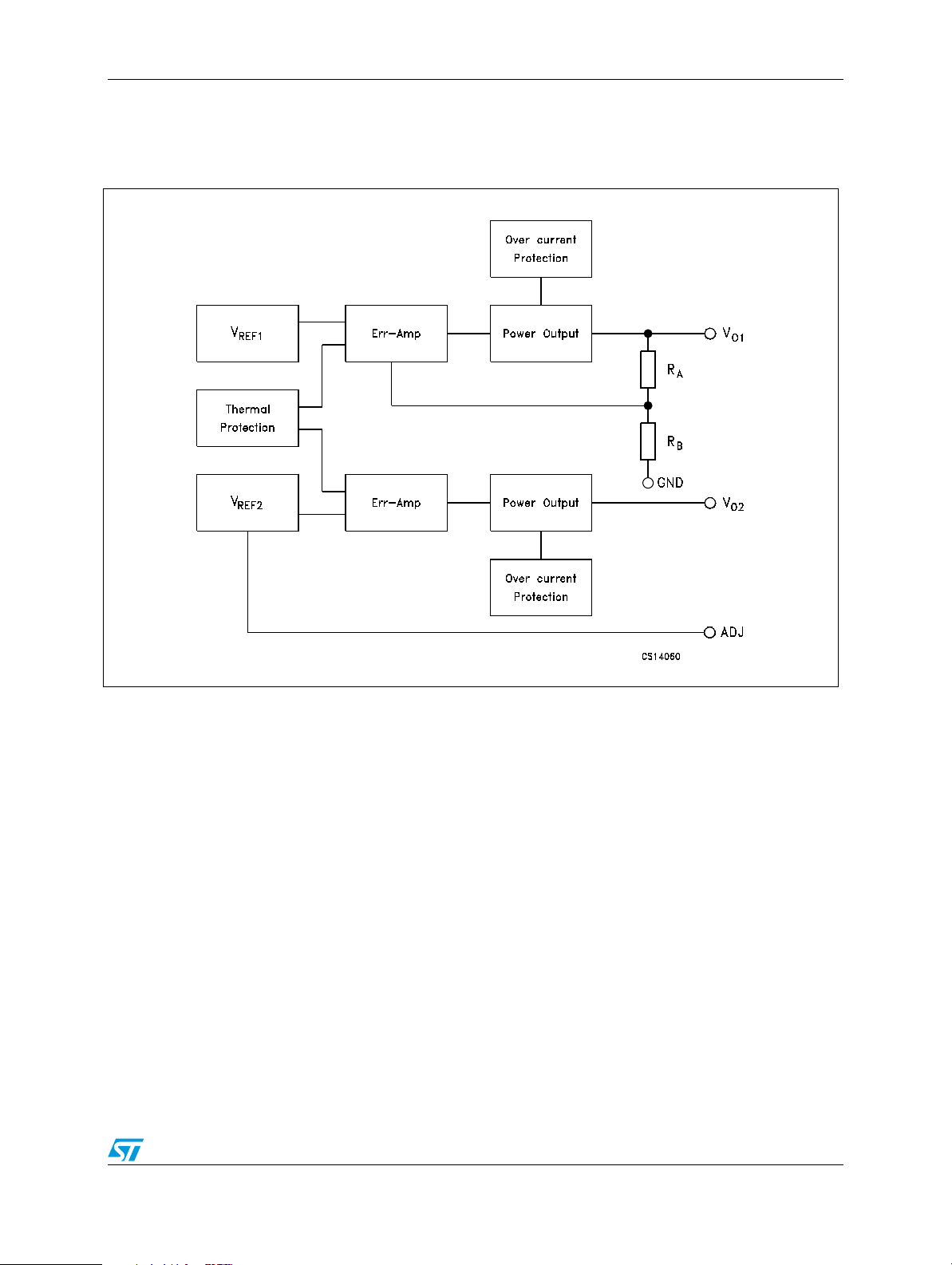
Figure 1. Block diagram of the fixed / adjustable output version of the ST2L05-3300
3/29
Page 4
Pin configuration ST2L05-3300
2 Pin configuration
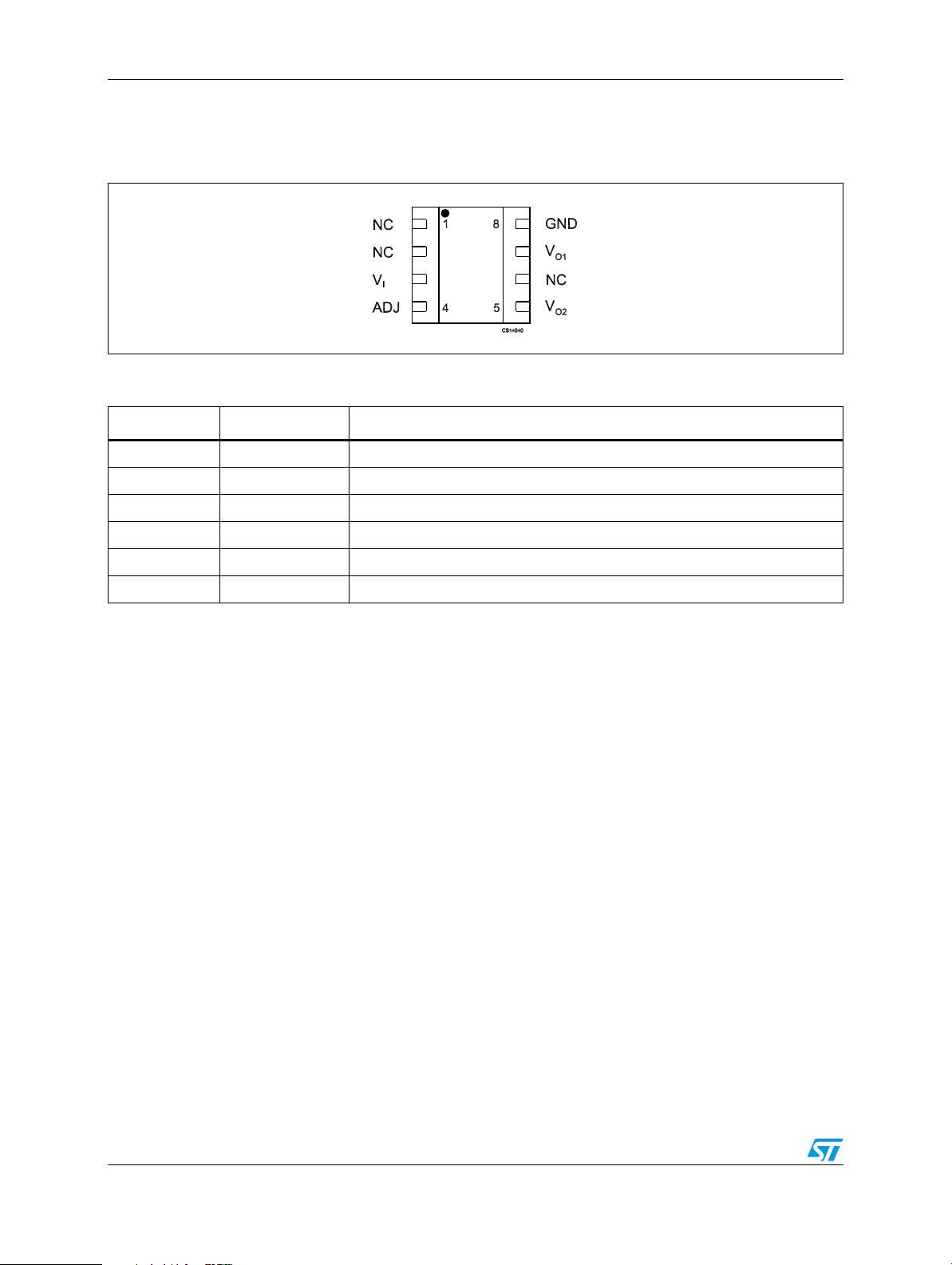
Figure 2. Pin connection (top through view)
Table 2. Pin description
Pin n° Symbol Name and function
3V
I
Bypass with a 4.7 µF capacitor to GND
4 ADJ Resistor divider connection
8 GND Ground
5V
7V
O2
O1
Adjustable output voltage: bypass with a 4.7 µF capacitor to GND
Fixed output voltage: bypass with a 4.7 µF capacitor to GND
1, 2, 6 NC Not connected
4/29
Page 5
ST2L05-3300 Maximum ratings
3 Maximum ratings
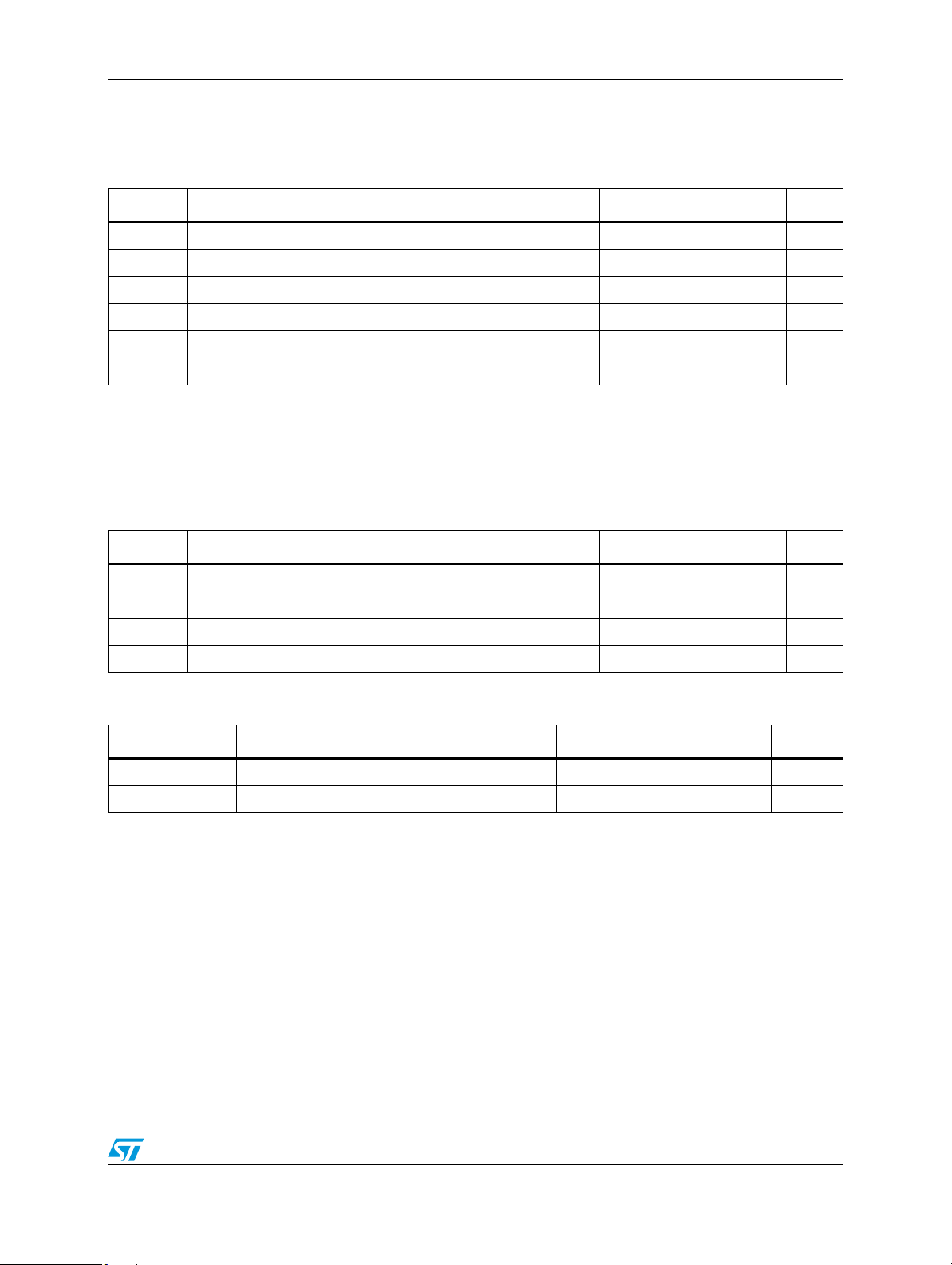
Table 3. Absolute maximum ratings
Symbol Parameter Value Unit
V
P
I
OSH
T
T
STG
T
LEAD
1. Storage temperatures > 125°C are only acceptable if the dual regulator is soldered to a PCBA.
Operating input voltage 10 V
I
Power dissipation Internally limited
D
Short circuit output current - 3.3 V and adjustable output Internally limited
Operating junction temperature range 0 to 150 °C
OP
Storage temperature range
(1)
- 65 to 150 °C
Lead temperature (soldering) 10 sec. 260 °C
Note: Absolute maximum ratings are those values beyond which damage to the device may occur.
Functional operation under these condition is not implied.
Table 4. Recommended operating conditions
Symbol Parameter Value Unit
V
ΔV
t
RISE
t
FAL L
Input voltage 4.5 to 7 V
I
Input voltage ripple ± 0.15 V
I
Input voltage rise time (from 10% to 90%) ≥ 1µs
Input voltage fall time (from 10% to 90%) ≥ 1µs
Table 5. Thermal data
Symbol Parameter Value Unit
R
thJC
R
thJA
Thermal resistance junction-case 2 °C/W
Thermal resistance junction-ambient 36 °C/W
5/29
Page 6
Application circuits ST2L05-3300
4 Application circuits
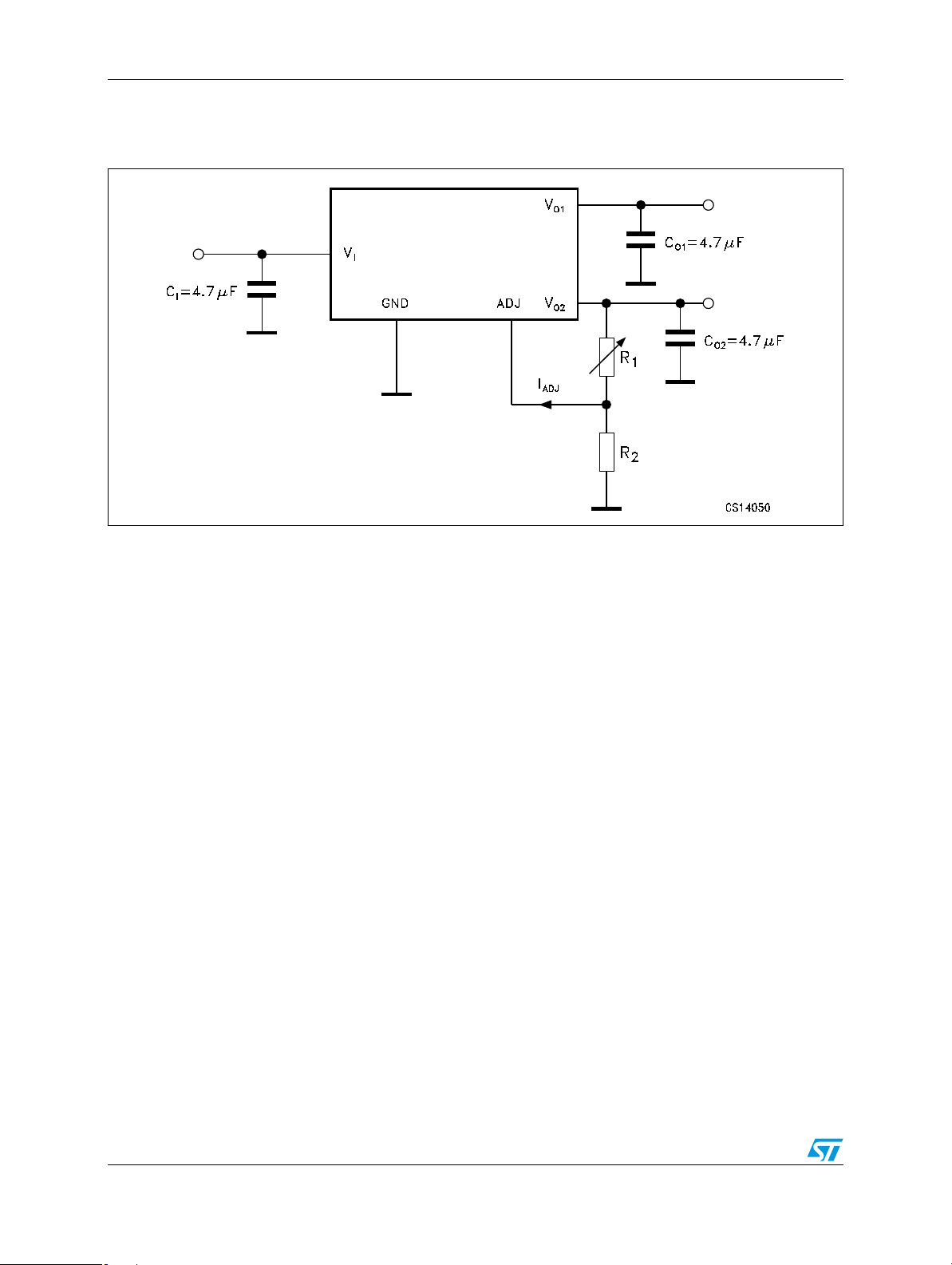
Figure 3. Application circuit of fixed / adj. version
1. In the fixed / adj. version, the adjustable output voltage V
V
. The adjustable output voltage VO2 is set using a resistor divider connected between VO2 (pin 4) and ground (pin 3)
DROP
with its center tap connected to VO2 ADJ (pin 2). The voltage divider resistors are: R1 connected to VO2 and VO2 ADJ and
R2 connected to VO2 ADJ and GND. VO2 is determined by V
application hints section):
V
= V
O2
(1 + R1 / R2) + I
REF
ADJR1
O2
(1)
is designed to support output voltages from 1.25 V to VI -
, R1, R2, and I
REF
as follows (for more details see the
ADJ
6/29
Page 7
ST2L05-3300 Electrical characteristics
5 Electrical characteristics
IO = 10 mA to 1 A, TJ = 0 to 125 °C, VI = 4.5 V to 7 V, CI = 4.7 µF, C
O1
= C
= 4.7 µF, unless
O2
otherwise specified.
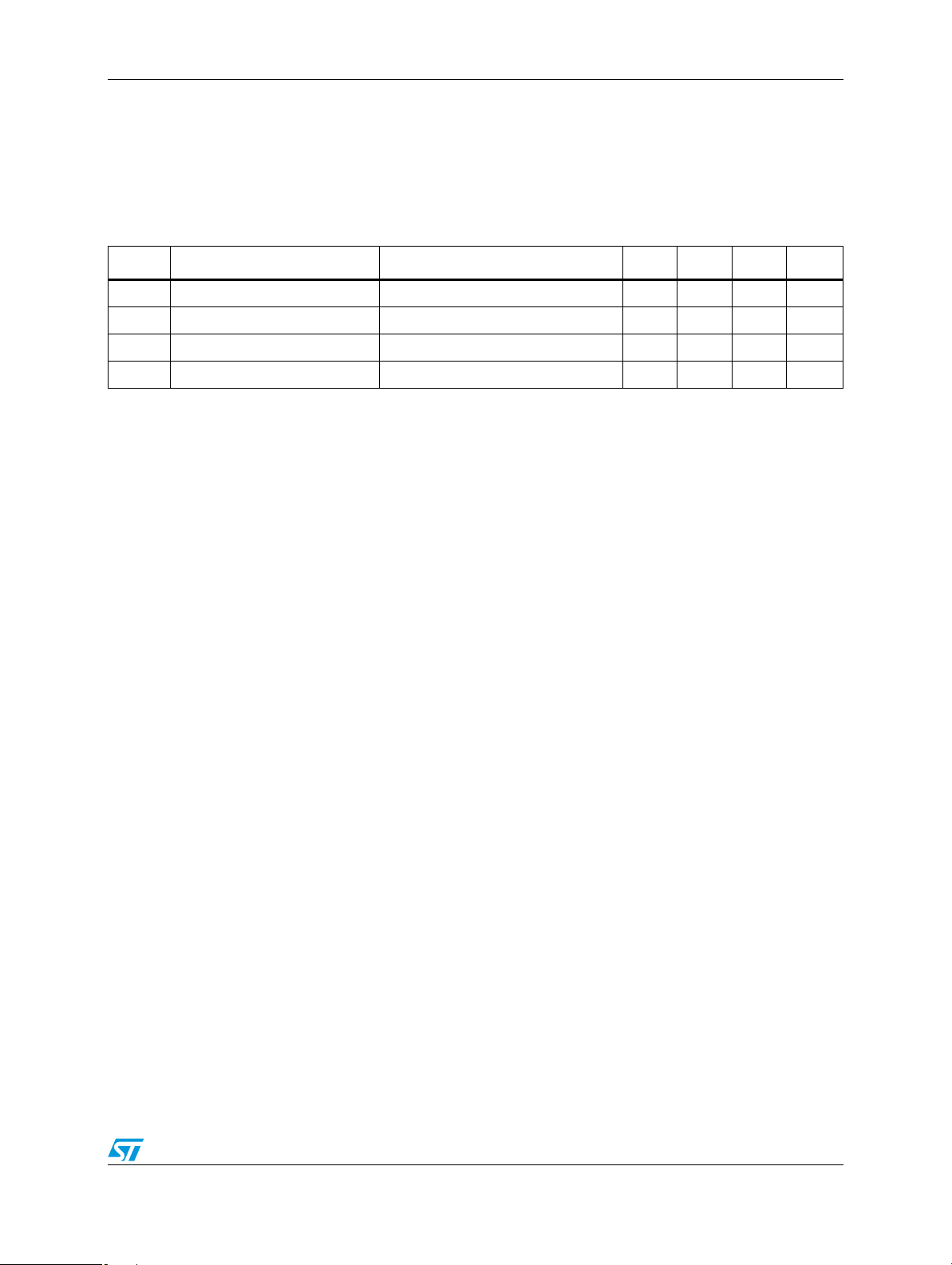
Table 6. Output 1 and output 2 dual specification
Symbol Parameter Test conditions Min. Typ. Max. Unit
I
GND
I
ST
T
SHDN
DT
SHDN
Quiescent current (fixed / adj.) VI ≤ 7 V, I
Total current limit I
O1
+ I
O2
= 5 mA to 1 A 5 mA
OUT1,2
2A
Thermal shutdown 175 °C
Thermal shutdown hysteresis 5 °C
7/29
Page 8
Electrical characteristics ST2L05-3300
IO = 10 mA to 1 A, TJ = 0 to 125 °C, VI = 4.5 V to 7 V, CI = 4.7 µF, C
O1
= C
= 4.7 µF, unless
O2
otherwise specified.
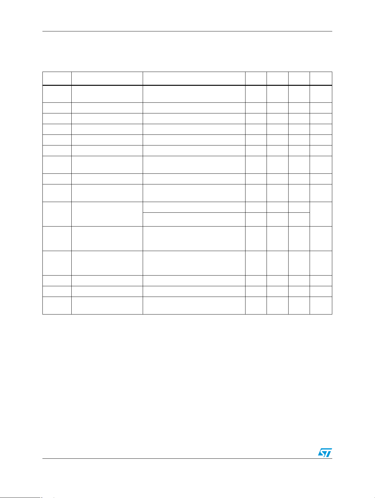
Table 7. Electrical characteristics of fixed output 1.5 V
Symbol Parameter Test conditions Min. Typ. Max. Unit
V
O
V
O
ΔV
O
ΔV
O
V
D
I
S
I
OMIN
e
N
SVR
ΔVO/ΔI
ΔVO1/ΔV
ΔV
/ΔI
O
T
R
S Temperature stability
S
= 5mA to 1A, VI = 4.75 to 5.25V
I
Output voltage 1.5V
O
T = 25°C
1.47 1.5 1.53 V
Output voltage 1.5V IO = 5mA to 1A, VI = 4.75 to 5.25V 1.455 1.5 1.545 V
Line regulation VI = 4.75 to 5.25V, IO = 5mA to 1A 15 mV
Load regulation VI = 4.75V, IO = 10mA to 1A 12 mV
Dropout voltage ΔVO = -1% IO = 1A 1.3 V
Current limit VI = 5.5V 1 A
Min. output current for
regulation
RMS output noise
Supply voltage
rejection
(2)(5)
Transient response change
of VO with step load
O
change
(3)(5)
Transient response change
of V
I
of V
with application
OUT1
(3)(5)
I
Transient response short
circuit removal response
O
(3)(5)
Thermal regulation
Long-term stability
(1000hrs)
(1) (5)
(5)
(5)
(5)
T = 25°C 0.003 %
VI = 5V 60 dB
VI = 5V, IO = 1mA to 1A, tr ≥ 1µs 10
= 5V, IO = 1A to 1mA, tf ≥ 1µs 10
V
I
0 to 5V step input, IO = 1mA to 1A,
tr ≥ 1µs
VI = 5V, IO = short to IO = 10mA 20
IO = 1A, t
= 30ms 0.1 %/W
PULSE
0.5 %
= 125°C 0.3 %
T
J
0mA
(4)
(4)
(4)
10
(4)
%
%
%
1. Bandwidth of 10 Hz to 10 kHz.
2. 120 Hz input ripple.
= 20 µF, CO1 and CO2 = 10 µF. CI, CO1 and CO2 are all X7R ceramic capacitors.
3. C
I
4. % undershoot or overshoot of V
5. Guaranteed by design, not tested in production.
O
8/29
Page 9
ST2L05-3300 Electrical characteristics
IO = 10 mA to 1 A, TJ = 0 to 125 °C, VI = 4.5 V to 7 V, CI = 4.7 µF, C
O1
= C
= 4.7 µF, unless
O2
otherwise specified.
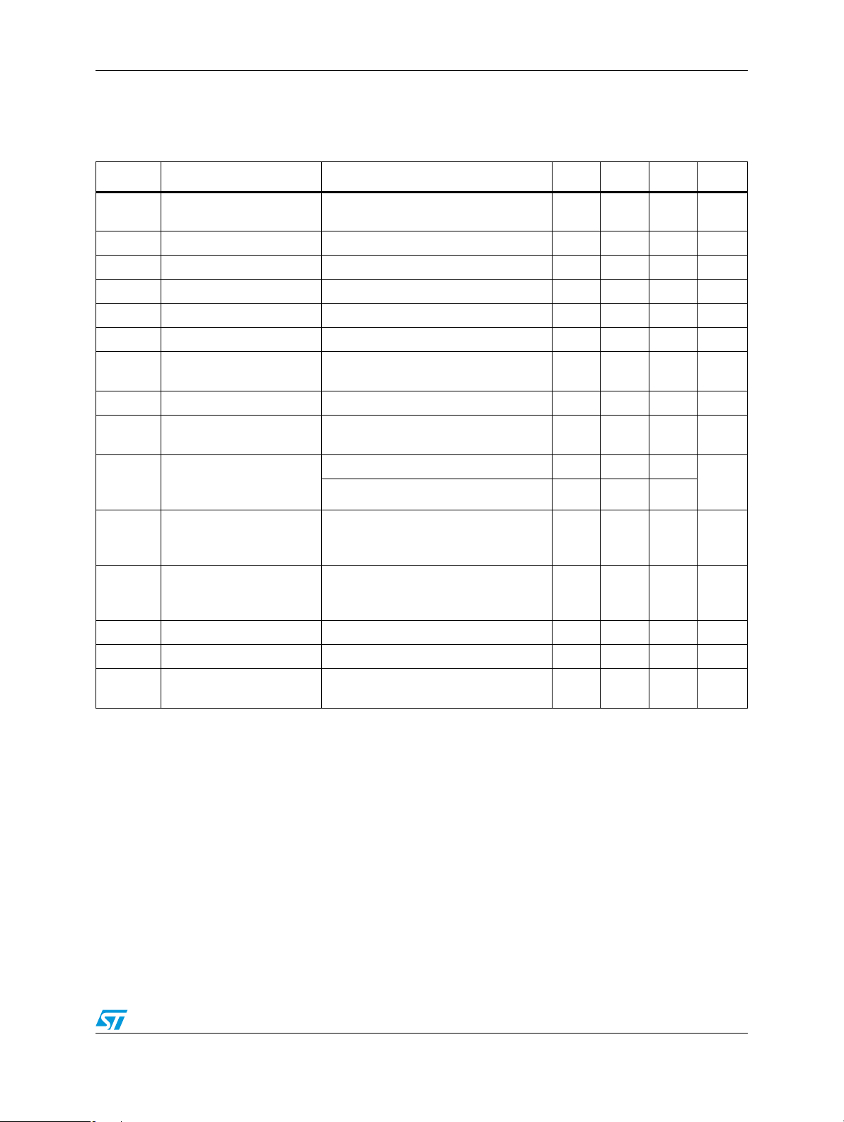
Table 8. Electrical characteristics of fixed output 1.8 V
Symbol Parameter Test conditions Min. Typ. Max. Unit
V
O
V
O
ΔV
O
ΔV
O
V
D
I
S
I
OMIN
e
N
SVR
ΔVO/ΔI
ΔVO1/ΔV
ΔV
/ΔI
O
T
R
S Temperature stability
S
= 5mA to 1A, VI = 4.75 to 5.25V
I
Output voltage 1.8V
O
T = 25°C
1.764 1.8 1.836 V
Output voltage 1.8V IO = 5mA to 1A, VI = 4.75 to 5.25V 1.746 1.8 1.854 V
Line regulation VI = 4.75 to 5.25V, IO = 5mA to 1A 15 mV
Load regulation VI = 4.75V, IO = 10mA to 1A 12 mV
Dropout voltage ΔVO = -1% IO = 1A 1.3 V
Current limit VI = 5.5V 1 A
Min. output current for
regulation
RMS output noise
Supply voltage
rejection
(2)(5)
Transient response change
of VO with step load
O
change
(3)(5)
Transient response change
of V
I
of V
with application
OUT1
(3)(5)
I
Transient response short
circuit removal response
O
(3)(5)
Thermal regulation
Long-term stability
(1000hrs)
(1) (5)
(5)
(5)
(5)
T = 25°C 0.003 %
VI = 5V 60 dB
VI = 5V, IO = 1mA to 1A, tr ≥ 1µs 10
= 5V, IO = 1A to 1mA, tf ≥ 1µs 10
V
I
0 to 5V step input, IO = 1mA to 1A,
tr ≥ 1µs
VI = 5V, IO = short to IO = 10mA 20
IO = 1A, t
= 30ms 0.1 %/W
PULSE
0.5 %
= 125°C 0.3 %
T
J
0mA
(4)
(4)
(4)
10
(4)
%
%
%
1. Bandwidth of 10 Hz to 10 kHz.
2. 120 Hz input ripple.
= 20 µF, CO1 and CO2 = 10 µF. CI, CO1 and CO2 are all X7R ceramic capacitors.
3. C
I
4. % undershoot or overshoot of V
5. Guaranteed by design, not tested in production.
O
9/29
Page 10
Electrical characteristics ST2L05-3300
IO = 10 mA to 1 A, TJ = 0 to 125 °C, VI = 4.5 V to 7 V, CI = 4.7 µF, C
O1
= C
= 4.7 µF, unless
O2
otherwise specified.
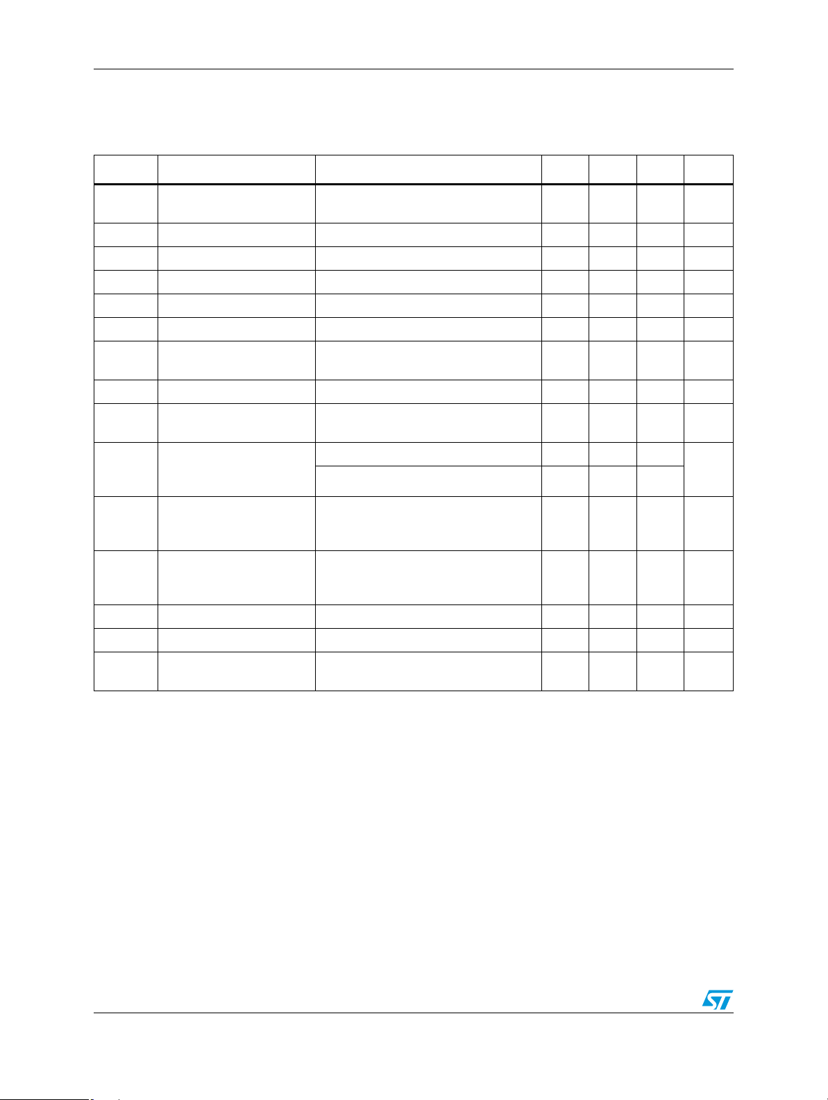
Table 9. Electrical characteristics of fixed output 2.5 V
Symbol Parameter Test conditions Min. Typ. Max. Unit
V
O
V
O
ΔV
O
ΔV
O
V
D
I
S
I
OMIN
e
N
SVR
/ΔI
ΔV
O
ΔVO1/ΔV
ΔV
/ΔI
O
T
R
S Temperature stability
S
= 5mA to 1A, VI = 4.75 to 5.25V
I
Output voltage 2.5V
O
T = 25°C
2.45 2.5 2.55 V
Output voltage 2.5V IO = 5mA to 1A, VI = 4.75 to 5.25V 2.425 2.5 2.575 V
Line regulation VI = 4.75 to 5.25V, IO = 5mA to 1A 15 mV
Load regulation VI = 4.75V, IO = 10mA to 1A 12 mV
Dropout voltage ΔVO = -1% IO = 1A 1.3 V
Current limit VI = 5.5V 1 A
Min. output current for
regulation
RMS output noise
Supply voltage
rejection
(2)(5)
Transient response change
O
O
change
(3)(5)
with step load
of V
Transient response change
I
of V
of VI
with application
OUT1
(3)(5)
Transient response short
circuit removal response
O
(3)(5)
Thermal regulation
Long-term stability
(1000hrs)
(1) (5)
(5)
(5)
(5)
T = 25°C 0.003 %
VI = 5V 60 dB
VI = 5V, IO = 1mA to 1A, tr ≥ 1µs 10
VI = 5V, IO = 1A to 1mA, tf ≥ 1µs 10
0 to 5V step input, IO= 1mA to 1A,
tr ≥ 1µs
VI = 5V, IO = short to IO = 10mA 20
IO = 1A, t
= 30ms 0.1 %/W
PULSE
0.5 %
T
= 125°C 0.3 %
J
0mA
(4)
(4)
(4)
10
(4)
%
%
%
1. Bandwidth of 10 Hz to 10 kHz.
2. 120 Hz input ripple.
= 20 µF, CO1 and CO2 = 10 µF. CI, CO1 and CO2 are all X7R ceramic capacitors.
3. C
I
4. % undershoot or overshoot of V
5. Guaranteed by design, not tested in production.
O
10/29
Page 11
ST2L05-3300 Electrical characteristics
IO = 10 mA to 1 A, TJ = 0 to 125 °C, VI = 4.5 V to 7 V, CI = 4.7 µF, C
O1
= C
= 4.7 µF, unless
O2
otherwise specified.
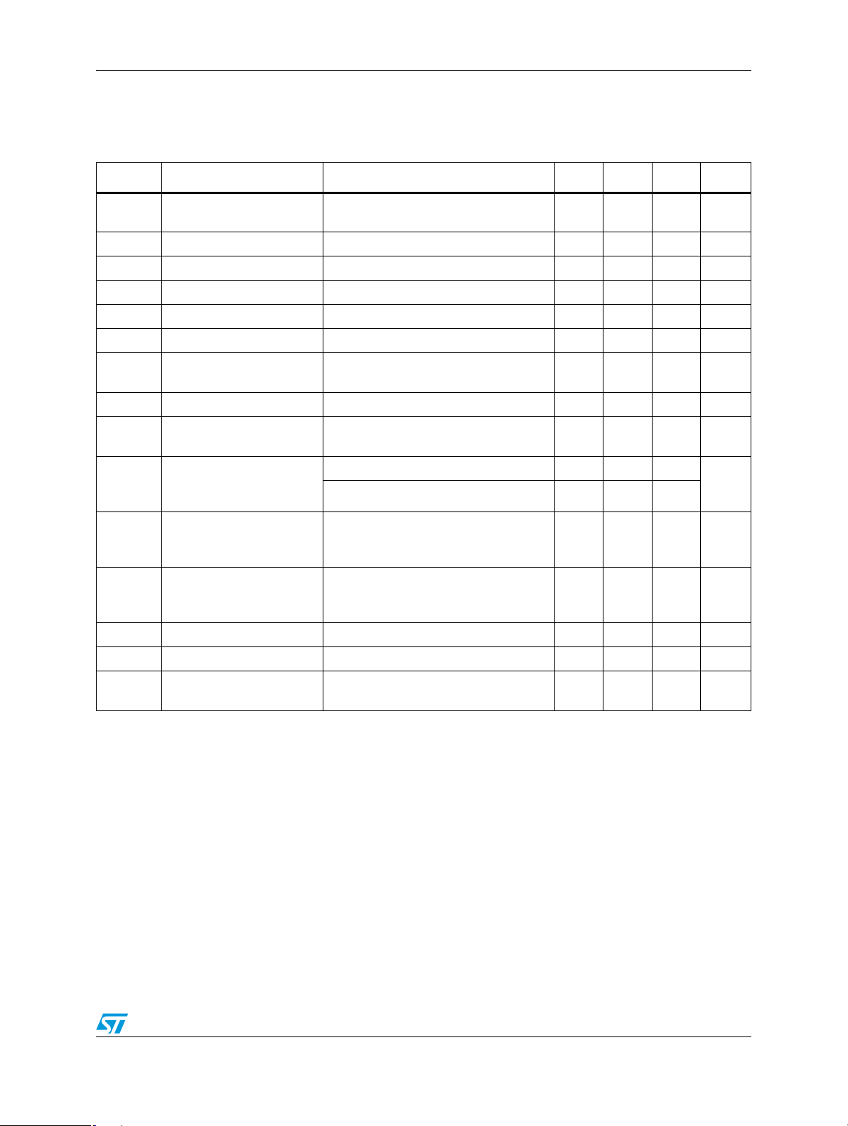
Table 10. Electrical characteristics of fixed output 2.8 V
Symbol Parameter Test conditions Min. Typ. Max. Unit
V
O
V
O
ΔV
O
ΔV
O
V
D
I
S
I
OMIN
e
N
SVR
ΔVO/ΔI
ΔVO1/ΔV
ΔV
/ΔI
O
T
R
S Temperature stability
S
= 5mA to 1A, VI = 4.75 to 5.25V
I
Output voltage 2.8V
O
T = 25°C
2.744 2.8 2.856 V
Output voltage 2.8V IO = 5mA to 1A, VI = 4.75 to 5.25V 2.716 2.8 2.884 V
Line regulation VI = 4.75 to 5.25V, IO = 5mA to 1A 15 mV
Load regulation VI = 4.75V, IO = 10mA to 1A 12 mV
Dropout voltage ΔVO = -1% IO = 1A 1.3 V
Current limit VI = 5.5V 1 A
Min. output current for
regulation
RMS output noise
Supply voltage
rejection
(2)(5)
Transient response change
of VO with step load
O
change
(3)(5)
Transient response change
of V
I
of V
with application
OUT1
(3)(5)
I
Transient response short
circuit removal response
O
(3)(5)
Thermal regulation
Long-term stability
(1000hrs)
(1) (5)
(5)
(5)
(5)
T = 25°C 0.003 %
VI = 5V 60 dB
VI = 5V, IO = 1mA to 1A, tr ≥ 1µs 10
= 5V, IO = 1A to 1mA, tf ≥ 1µs 10
V
I
0 to 5V step input, IO= 1mA to 1A,
tr ≥ 1µs
VI = 5V, IO = short to IO = 10mA 20
IO = 1A, t
= 30ms 0.1 %/W
PULSE
0.5 %
= 125°C 0.3 %
T
J
0mA
(4)
(4)
(4)
10
(4)
%
%
%
1. Bandwidth of 10 Hz to 10 kHz.
2. 120 Hz input ripple.
= 20 µF, CO1 and CO2 = 10 µF. CI, CO1 and CO2 are all X7R ceramic capacitors.
3. C
I
4. % undershoot or overshoot of V
5. Guaranteed by design, not tested in production.
O
11/29
Page 12
Electrical characteristics ST2L05-3300
IO = 10 mA to 1 A, TJ = 0 to 125 °C, VI = 4.5 V to 7 V, CI = 4.7 µF, C
O1
= C
= 4.7 µF, unless
O2
otherwise specified.
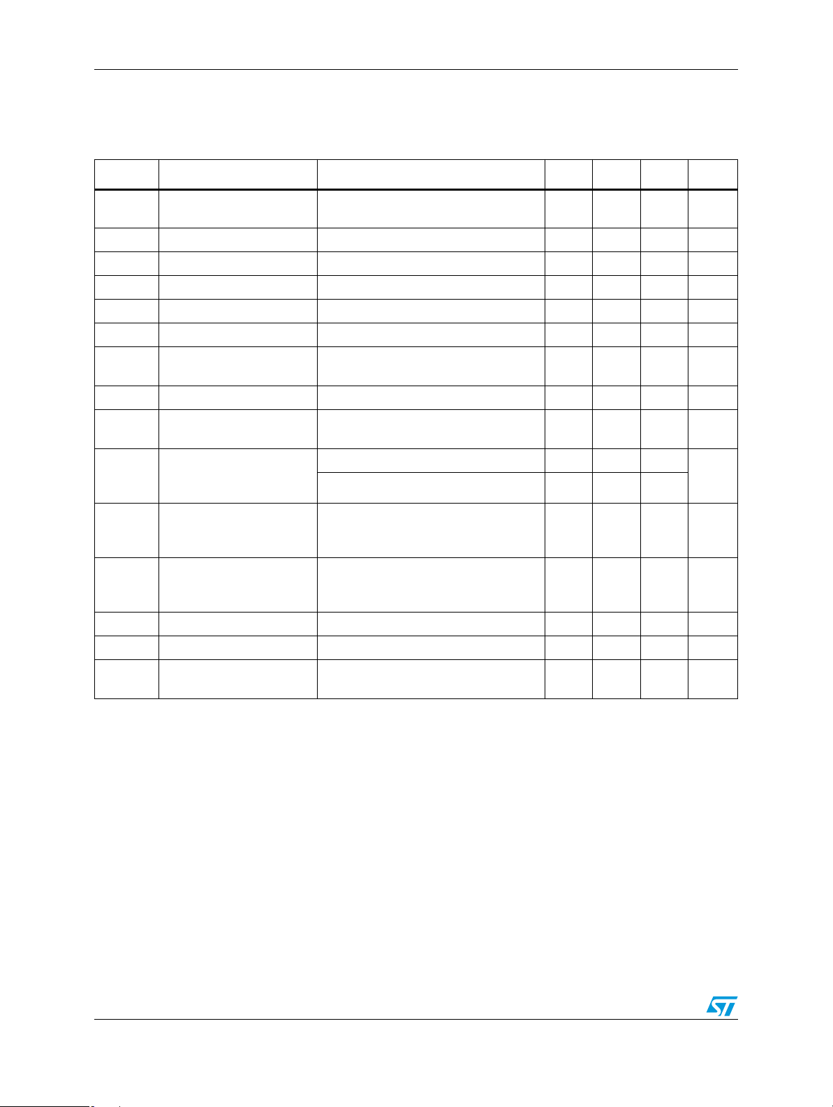
Table 11. Electrical characteristics of fixed output 3.0 V
Symbol Parameter Test conditions Min. Typ. Max. Unit
V
O
V
O
ΔV
O
ΔV
O
V
D
I
S
I
OMIN
e
N
SVR
ΔVO/ΔI
ΔVO1/ΔV
ΔV
/ΔI
O
T
R
S Temperature stability
S
= 5mA to 1A, VI = 4.75 to 5.25V
I
Output voltage 3.0V
O
T = 25°C
2.94 3.0 3.06 V
Output voltage 3.0V IO = 5mA to 1A, VI = 4.75 to 5.25V 2.91 3.0 3.09 V
Line regulation VI = 4.75 to 5.25V, IO = 5mA to 1A 15 mV
Load regulation VI = 4.75V, IO = 10mA to 1A 12 mV
Dropout voltage ΔVO = -1% IO = 1A 1.3 V
Current limit VI = 5.5V 1 A
Min. output current for
regulation
RMS output noise
Supply voltage
rejection
(2)(5)
Transient response change
of VO with step load
O
change
(3)(5)
Transient response change
of V
I
of V
with application
OUT1
(3)(5)
I
Transient response short
circuit removal response
O
(3)(5)
Thermal regulation
Long-term stability
(1000hrs)
(1) (5)
(5)
(5)
(5)
T = 25°C 0.003 %
VI = 5V 60 dB
VI = 5V, IO = 1mA to 1A, tr ≥ 1µs 10
= 5V, IO = 1A to 1mA, tf ≥ 1µs 10
V
I
0 to 5V step input, IO= 1mA to 1A,
tr ≥ 1µs
VI = 5V, IO = short to IO = 10mA 20
IO = 1A, t
= 30ms 0.1 %/W
PULSE
0.5 %
= 125°C 0.3 %
T
J
0mA
(4)
(4)
(4)
10
(4)
%
%
%
1. Bandwidth of 10 Hz to 10 kHz.
2. 120 Hz input ripple.
= 20 µF, CO1 and CO2 = 10 µF. CI, CO1 and CO2 are all X7R ceramic capacitors.
3. C
I
4. % undershoot or overshoot of V
5. Guaranteed by design, not tested in production.
O
12/29
Page 13
ST2L05-3300 Electrical characteristics
IO = 10 mA to 1 A, TJ = 0 to 125 °C, VI = 4.5 V to 7 V, CI = 4.7 µF, C
O1
= C
= 4.7 µF, unless
O2
otherwise specified.
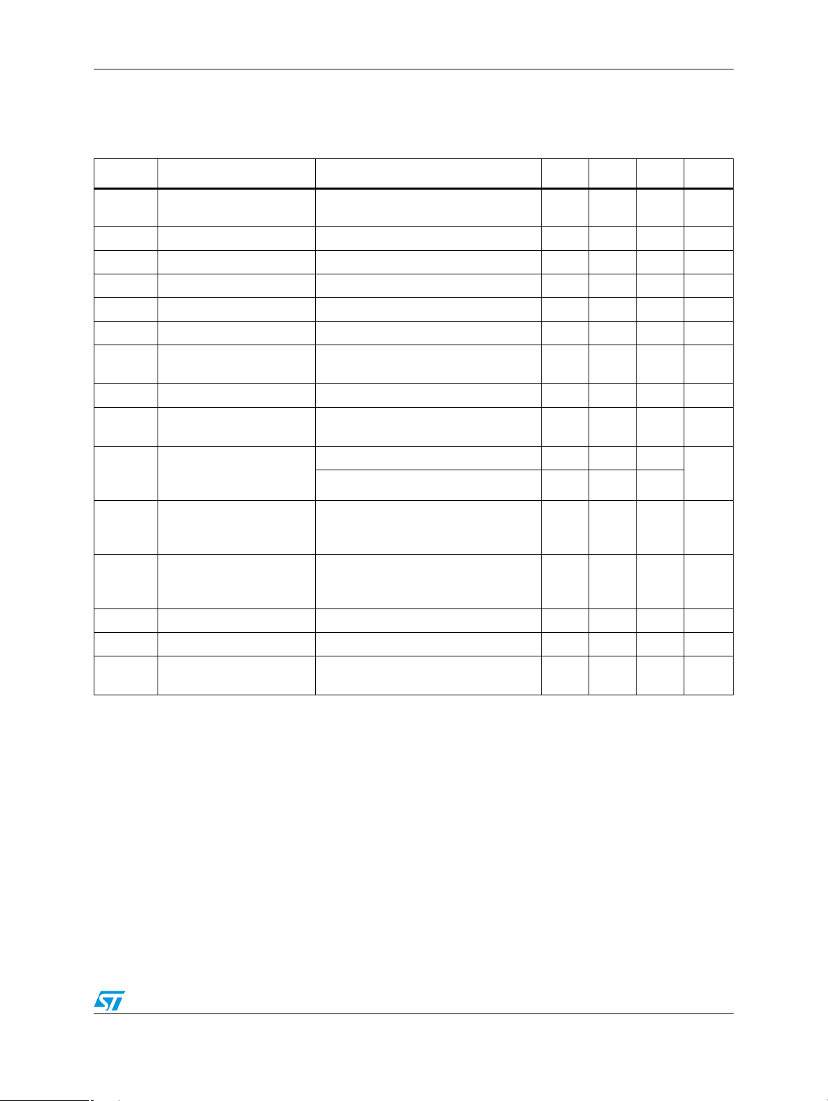
Table 12. Electrical characteristics of fixed output 3.3 V
Symbol Parameter Test Conditions Min. Typ. Max. Unit
V
O
V
O
ΔV
O
ΔV
O
V
D
I
S
I
OMIN
e
N
SVR
ΔVO/ΔI
ΔVO1/ΔV
ΔV
/ΔI
O
T
R
S Temperature stability
S
= 5mA to 1A, VI = 4.75 to 5.25V
I
Output voltage 3.3V
O
T = 25°C
3.234 3.3 3.366 V
Output voltage 3.3V IO = 5mA to 1A, VI = 4.75 to 5.25V 3.2 3.3 3.4 V
Line regulation VI = 4.75 to 5.25V, IO = 5mA to 1A 15 mV
Load regulation VI = 4.75V, IO = 10mA to 1A 12 mV
Dropout voltage ΔVO = -1% IO = 1A 1.3 V
Current limit VI = 5.5V 1 A
Min. output current for
regulation
RMS output noise
Supply voltage
rejection
(2)(5)
Transient response change
of VO with step load
O
change
(3)(5)
Transient response change
of V
I
of V
with application
OUT1
(3)(5)
I
Transient response short
circuit removal response
O
(3)(5)
Thermal regulation
Long-term stability
(1000hrs)
(1) (5)
(5)
(5)
(5)
T = 25°C 0.003 %
VI = 5V 60 dB
VI = 5V, IO = 1mA to 1A, tr ≥ 1µs 10
= 5V, IO = 1A to 1mA, tf ≥ 1µs 10
V
I
0 to 5V step input, IO= 1mA to 1A,
tr ≥ 1µs
VI = 5V, IO = short to IO = 10mA 20
IO = 1A, t
= 30ms 0.1 %/W
PULSE
0.5 %
= 125°C 0.3 %
T
J
0mA
(4)
(4)
(4)
10
(4)
%
%
%
1. Bandwidth of 10 Hz to 10 kHz.
2. 120 Hz input ripple.
= 20 µF, CO1 and CO2 = 10 µF. CI, CO1 and CO2 are all X7R ceramic capacitors.
3. C
I
4. % undershoot or overshoot of V
5. Guaranteed by design, not tested in production.
O
13/29
Page 14
Electrical characteristics ST2L05-3300
IO = 10 mA to 1 A, TJ = 0 to 125 °C, VI = 4.5 V to 7 V, CI = 4.7 µF, C
O1
= C
= 4.7 µF, unless
O2
otherwise specified.
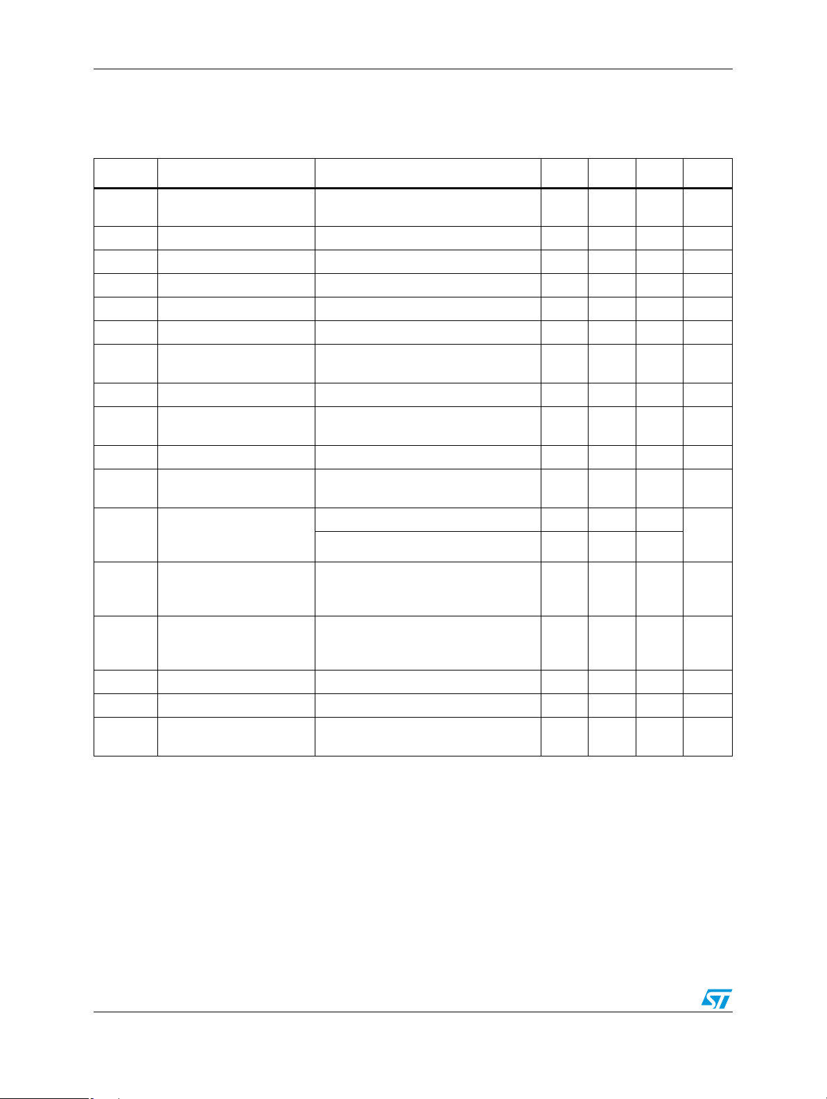
Table 13. Electrical characteristics of adjustable output
Symbol Parameter Test conditions Min. Typ. Max. Unit
V
O
V
O
ΔV
O2
ΔV
O2
V
D
I
S
I
ADJ
I
ΔADJ
I
OMIN
e
N
SVR
ΔV
/ΔI
O2
2
ΔVO2/ΔV
/ΔI
ΔV
O2
2
T
R
S Temperature stability
S
= 5mA to 1A, VI = 4.75 to 5.25V,
I
Reference voltage
O
T = 25°C
1.225 1.25 1.275 V
Reference voltage IO = 5mA to 1A, VI = 4.75 to 5.25V 1.212 1.25 1.287 V
Line regulation 2 VI = 4.75 to 5.25V, IO = 5mA to 1A 0.35 %
Load regulation 2 VI = 4.75V, IO = 10mA to 1A 0.4 %
Dropout voltage ΔVO = -1% IO = 1A 1.3 V
Current limit VI = 5.5V 1 A
Adjustable current
(sinking)
1µA
Adjustable current change IO = 10mA to 1A 200 nA
Min. output current for
regulation
RMS output noise
Supply voltage
rejection
Transient response change
O
of VO with step load
change
(2)(5)
(3)(5)
Transient response change
of V
I
of V
Transient response short
O
circuit removal response
(3)(5)
with application
OUT1
(3)(5)
I
Thermal regulation
Long-term stability
(1000hrs)
(1) (5)
(5)
(5)
(5)
T = 25°C 0.003 %
VI = 5V 60 dB
VI = 5V, IO = 1mA to 1A, tr ≥ 1µs 10
= 5V, IO = 1A to 1mA, tf ≥ 1µs 10
V
I
0 to 5V step input, IO= 1mA to 1A,
tr ≥ 1µs
VI = 5V, IO = short to IO = 10mA 20
IO = 1A, t
= 30ms 0.1 %/W
PULSE
0.5 %
T
= 125°C 0.3 %
J
2mA
(4)
(4)
(4)
10
(4)
%
%
%
1. Bandwidth of 10 Hz to 10 kHz.
2. 120 Hz input ripple.
= 20 µF, CO1 and CO2 = 10 µF. CI, CO1 and CO2 are all X7R ceramic capacitors.
3. C
I
4. % undershoot or overshoot of V
5. Guaranteed by design, not tested in production.
O
14/29
Page 15

ST2L05-3300 Application hints
6 Application hints
6.1 External capacitors
Like any low-dropout regulator, the ST2L05-3300 requires external capacitors for stability. It
is recommended to solder both capacitors as close as possible to the relative pins (1, 4 and
5).
6.2 Input capacitor
An input capacitor with a value of at least 2.2 µF is required. The amount of input
capacitance can be increased without limit if a good quality tantalum or aluminium capacitor
is used. SMD X7R or Y5V ceramic multilayer capacitors may not ensure stability in any
condition due to the variability of their frequency and temperature characteristics. The use of
this capacitor type is strictly related to the use of the output capacitors. For additional
details, please read the Output capacitor section below. The input capacitor must be located
at a distance of not more than 0.5" from the input pin of the device and returned to a clean
analog ground.
6.3 Output capacitor
The ST2L05-3300 is designed specifically to work with ceramic and tantalum capacitors.
Special care must be taken when a ceramic multilayer capacitor is used. Due to their
characteristics, this type of capacitor can sometimes have an ESR value lower than the
minimum required by the ST2L05-3300, and their relatively large capacitance can vary
greatly depending on the ambient temperature. The test results for the stability of the
ST2L05-3300 using multilayer ceramic capacitors show that a minimum value of 2.2 µF is
needed for both regulators. This value can be increased without limit if the input capacitor
value is greater than or equal to 4.7 µF, and up to 10 µF if the input capacitor is less than 4.7
µF. Surface-mountable solid tantalum capacitors offer a good combination of small physical
size, capacitance value and ESR in the range needed for the ST2L05-3300. Test results
show good stability for both outputs with values of at least 1 µF. The value can be increased
without limit for even better performance in areas such as transient response and noise.
Important:
The output capacitor must maintain an ESR in the stable region over the full operating
temperature to assure stability. Moreover, capacitor tolerance and variations due to
temperature must be considered to assure that the minimum amount of capacitance is
provided at all times. For this reason, when a ceramic multilayer capacitor is used, the better
choice for temperature coefficient is the X7R type, which holds the capacitance within ±
15%. The output capacitor should be located not more than 0.5" from the output pins of the
device and returned to a clean analog ground.
6.4 Adjustable regulator
The ST2L05-3300 has a 1.25 V reference voltage between the output and the adjust pins
(pins 4 and 2, respectively). When resistor R
constant current flows through R
voltage. Minimum load current is 2 mA max in all temperature conditions.
is placed between these two terminals, a
and down to R2 to set the overall (VO2 to GND) output
1
1
15/29
Page 16
Application hints ST2L05-3300
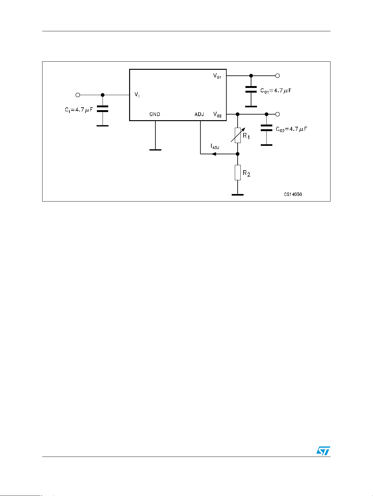
Figure 4. Application circuit
VO = V
I
is very small (typically 35 µA) and constant: in the VO calculation it can be ignored.
ADJ
(1 + R1 / R2) + I
REF
ADJR1
16/29
Page 17
ST2L05-3300 Typical characteristics
7 Typical characteristics
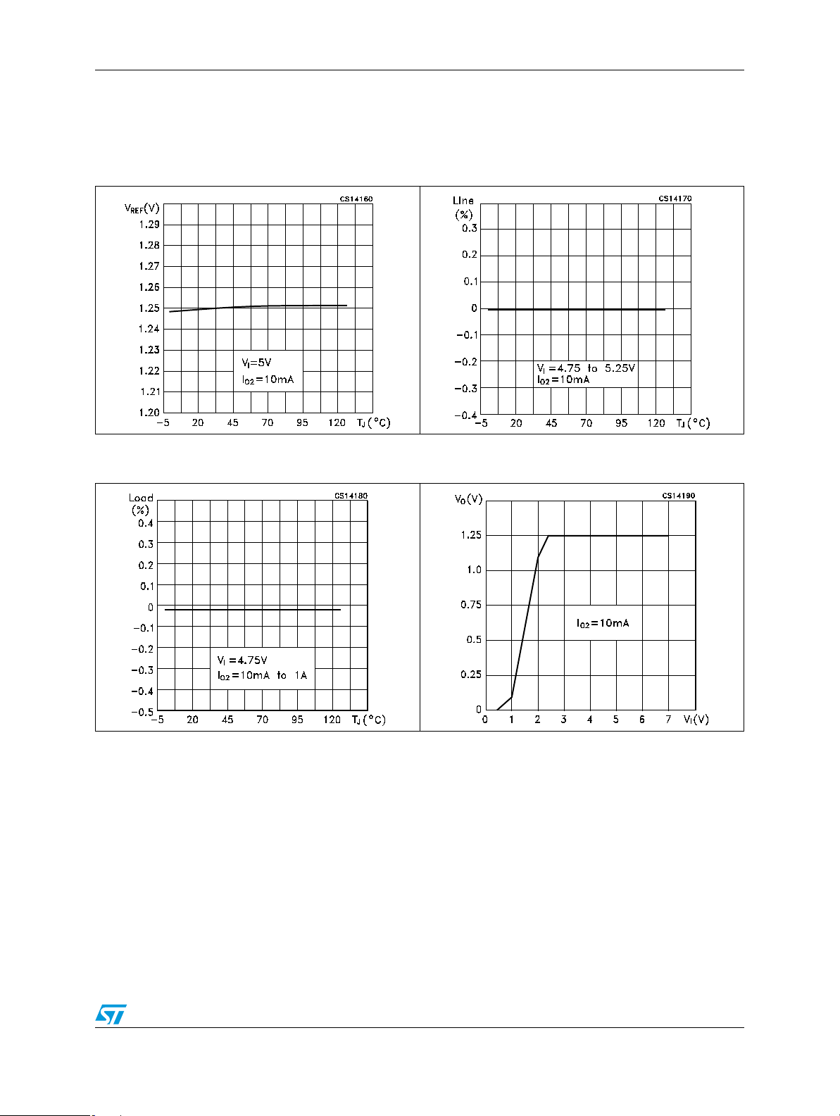
Figure 5. Reference voltage vs. temperature Figure 6. Reference line regulation vs.
temperature
Figure 7. Reference load regulation vs.
temperature
Figure 8. Reference voltage vs. input voltage
17/29
Page 18
Typical characteristics ST2L05-3300
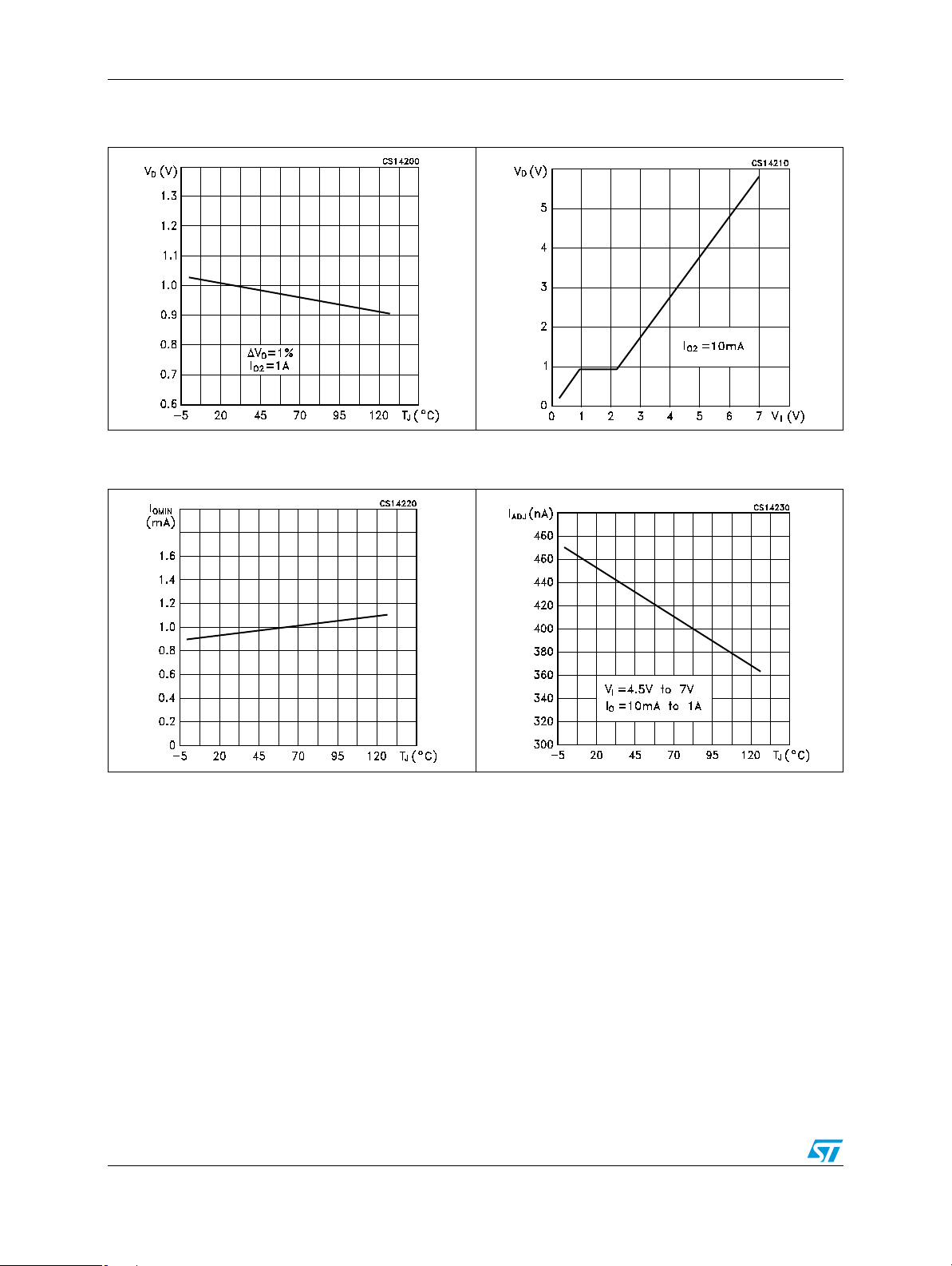
Figure 9. Dropout voltage vs. temperature
(adjustable output)
Figure 11. Minimum load current vs.
temperature (adjustable output)
Figure 10. Dropout voltage vs. input voltage
(adjustable output)
Figure 12. Adjust pin current vs. temperature
(adjustable output)
18/29
Page 19
ST2L05-3300 Typical characteristics
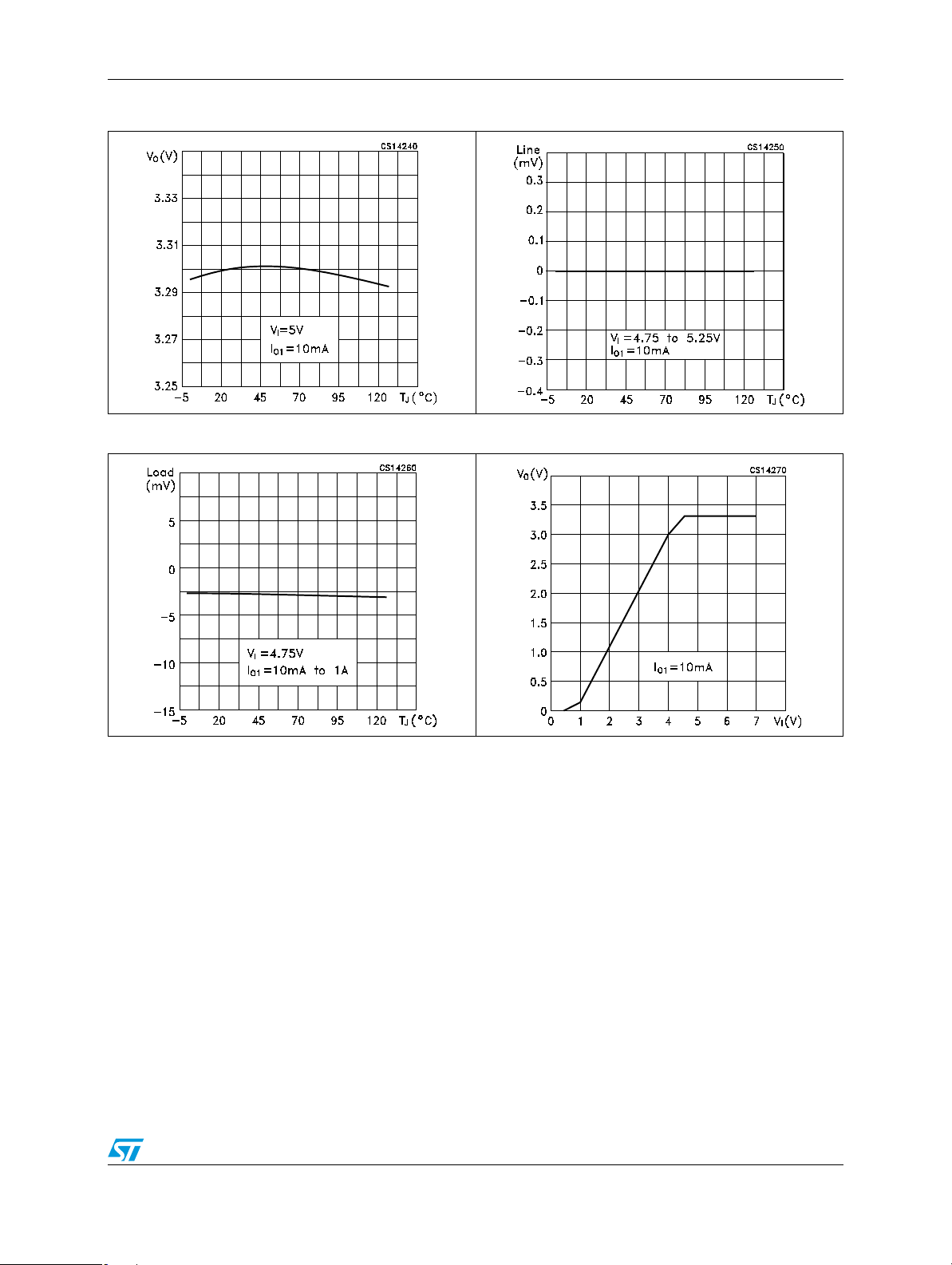
Figure 13. Output voltage vs. temperature Figure 14. Line regulation vs. temperature
Figure 15. Load regulation vs. temperature Figure 16. Output voltage vs. input voltage
19/29
Page 20
Typical characteristics ST2L05-3300
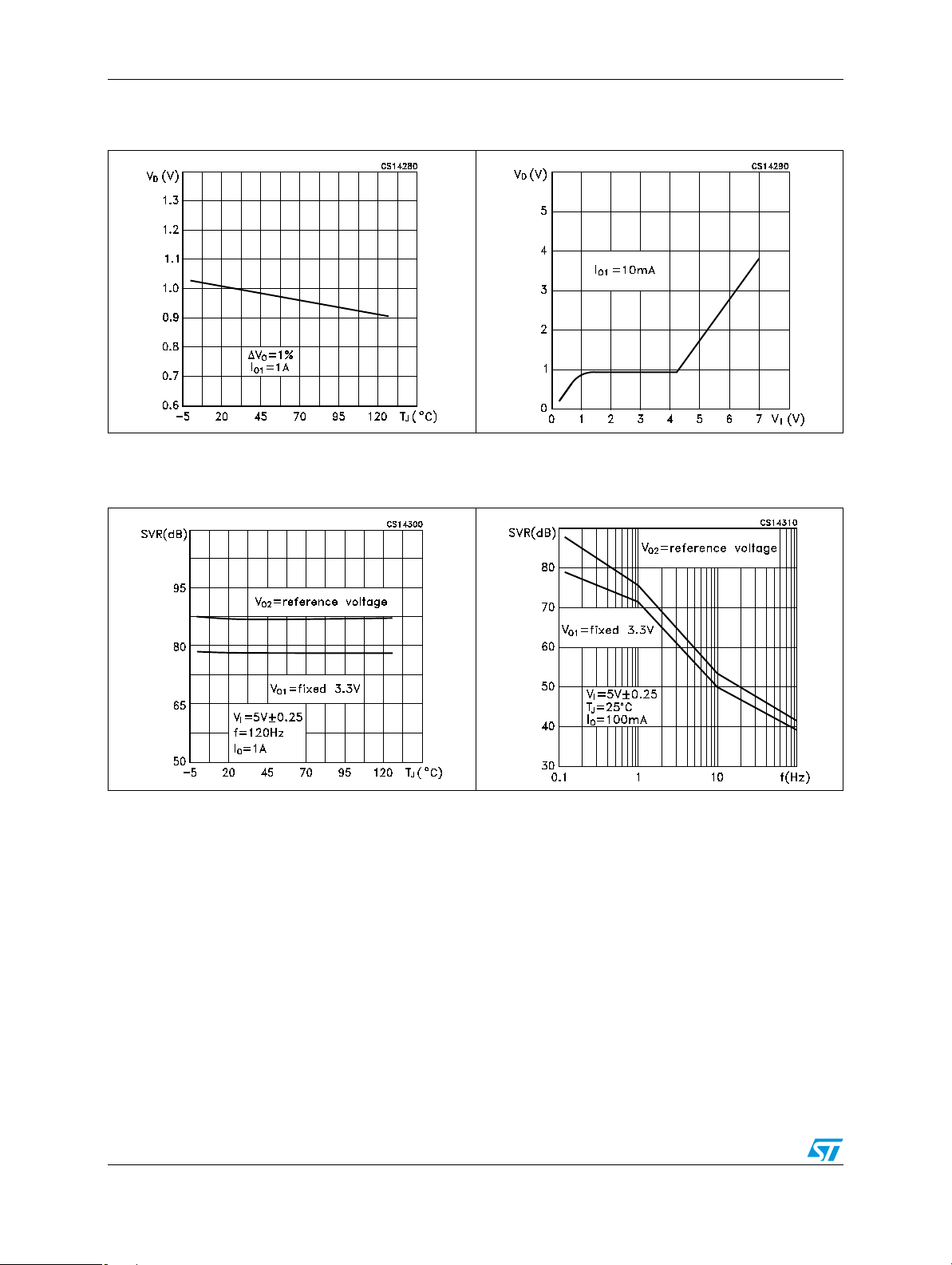
Figure 17. Dropout voltage vs. temperature
(fixed output)
Figure 19. Supply voltage rejection vs.
temperature
Figure 18. Dropout voltage vs. input voltage
Figure 20. Supply voltage rejection vs.
frequency
20/29
Page 21
ST2L05-3300 Typical characteristics
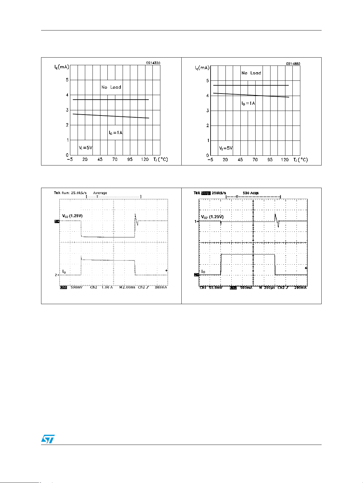
Figure 21. Quiescent current vs. temperature
(fixed/adj. version)
Figure 22. Quiescent current vs. temperature
(fixed/fixed version)
Figure 23. Short-circuit removal response Figure 24. Change of VO with step load
change
VI = 5 V, IO = short circuit to 10 mA, CO = 10 µF, CI = 22 µF
all ceramic X5R, T
= 25 °C
J
VI = 5 V, IO = 1 mA to 1 A, CO = 10 µF, CI = 22 µF all ceramic
X5R, T
= 25 °C
J
21/29
Page 22
Typical characteristics ST2L05-3300
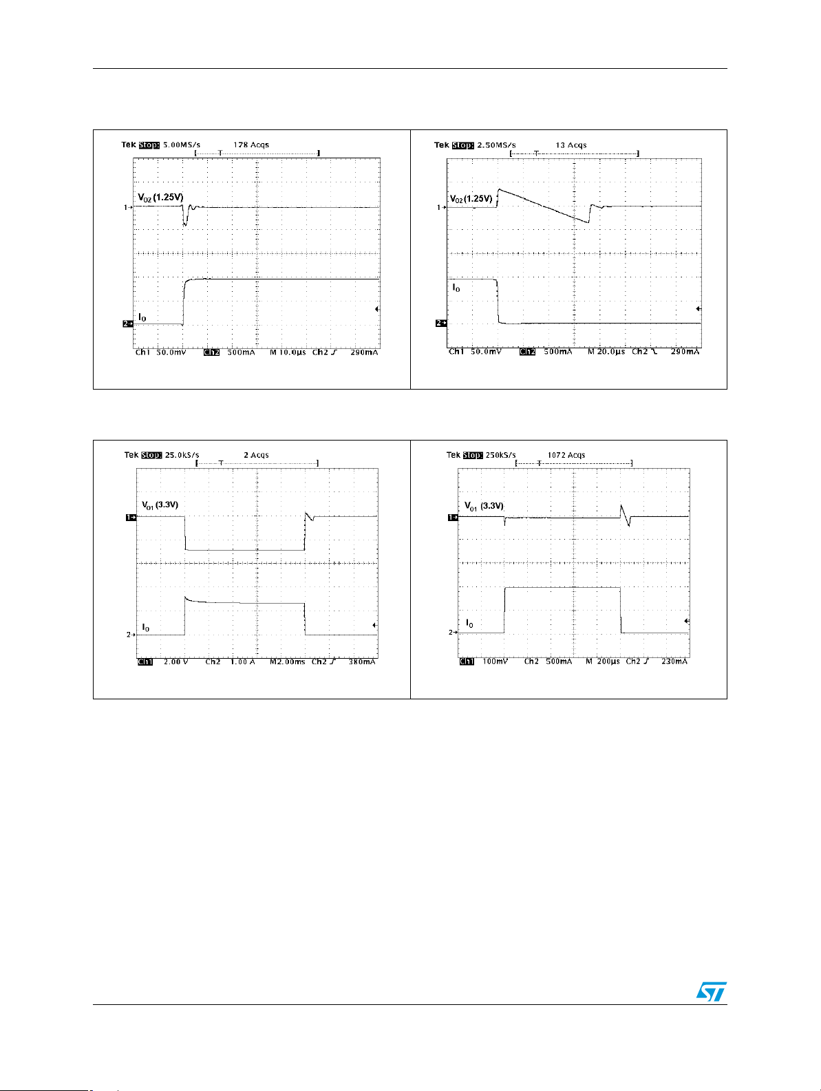
Figure 25. Change of VO with step load
VI = 5 V, IO = 1 mA to 1 A, CO = 10 µF, CI = 22 µF all
ceramic X5R, T
change
= 25 °C, t
J
RISE
= 1 µs
Figure 26. Change of VO with step load
VI = 5 V, IO = 1 mA to 1 A, CO = 10 µF, CI = 22 µF all
ceramic X5R, T
change
= 25 °C, t
J
FALL
= 1 µs
Figure 27. Short-circuit removal response Figure 28. Change of VO with step load
change
VI = 5 V, IO = short circuit to 10 mA, CO = 10 µF, CI = 22 µF
all ceramic X5R, T
= 25 °C
J
22/29
CO = CI = 4.7 µF, V
= 0 to 2 V, VI = 5.5 V, IO = 5 mA
EN
Page 23
ST2L05-3300 Typical characteristics
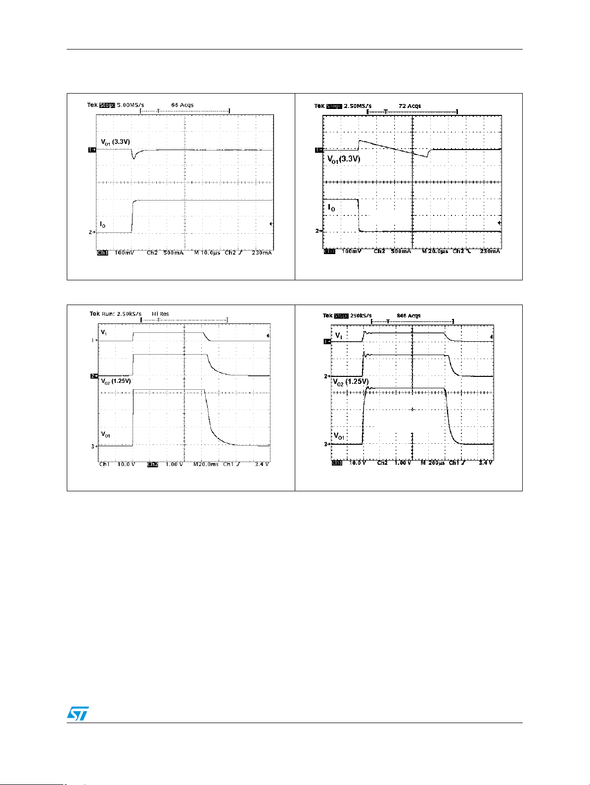
Figure 29. Change of VO with step load change Figure 30. Change of VO with step load
VI = 5 V, IO = 1 mA to 1 A, CO = 10 µF, CI = 22 µF all
ceramic X5R, T
Figure 31. Start-up transient Figure 32. Start-up transient
= 25 °C, t
J
RISE
= t
FALL
= 1 µs
VI = 5 V, IO = 1 mA to 1 A, CO = 10 µF, C I = 22 µF all
ceramic X5R, T
change
= 25 °C, t
J
FALL
= 1 µs
VI = 0 to 5 V, IO = 1 A, CO = 10 µF, CI = 22 µF all ceramic
X5R, T
= 25 °C, t
J
RISE
≤ 1 µs
VI = 0 to 5 V, IO = 1 A, CO = 10 µF, CI = 22 µF all ceramic
X5R, T
= 25 °C, t
J
RISE
≤ 1 µs
23/29
Page 24

Package mechanical data ST2L05-3300
8 Package mechanical data
In order to meet environmental requirements, ST offers these devices in different grades of
ECOPACK
specifications, grade definitions and product status are available at: www.st.com. ECOPACK
is an ST trademark.
®
packages, depending on their level of environmental compliance. ECOPACK®
24/29
Page 25
ST2L05-3300 Package mechanical data
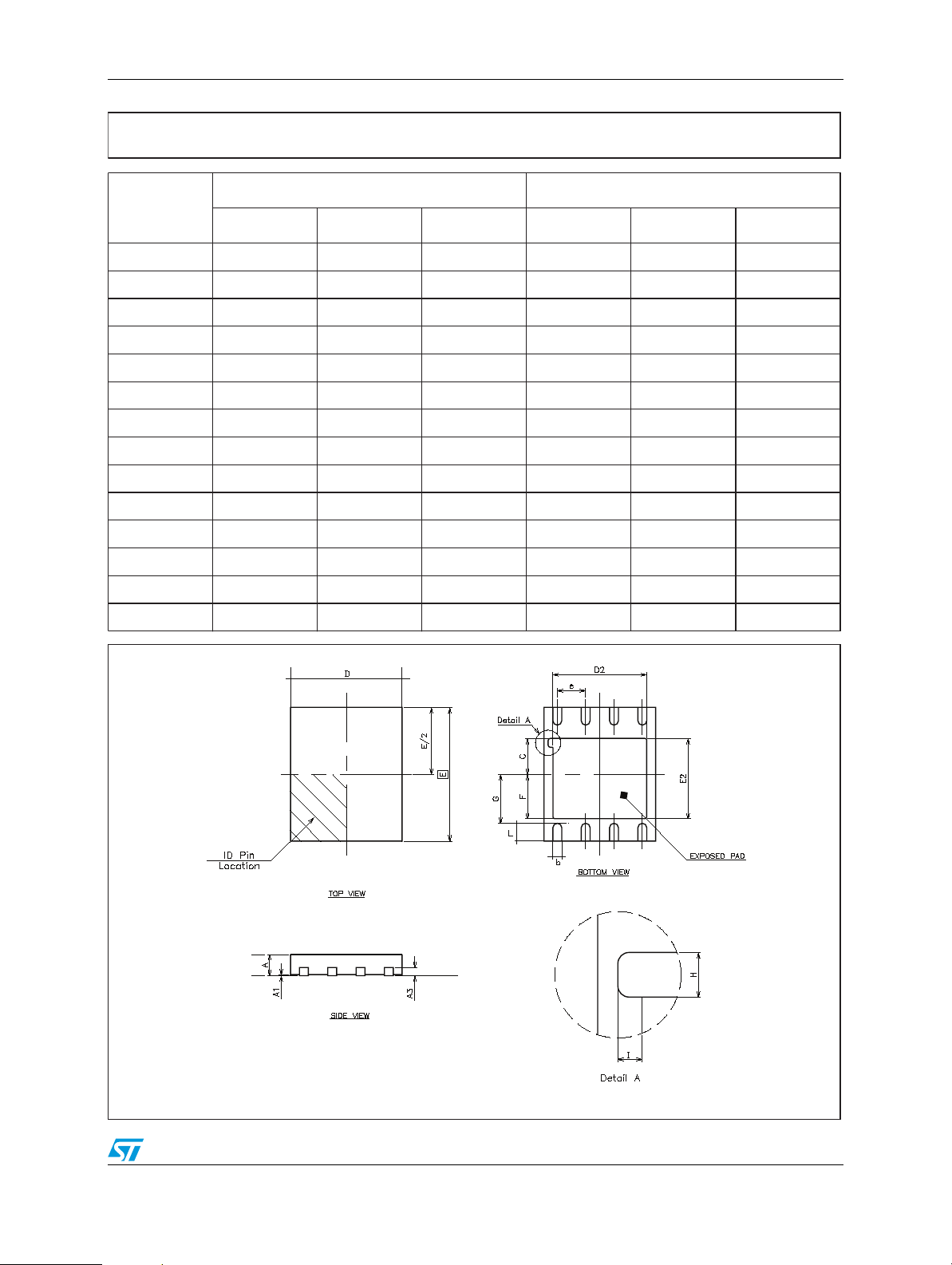
DFN8 (5x6 mm) mechanical data
mm. inch.
Dim.
Min. Typ. Max. Min. Typ. Max.
A0.800.90 1.00 0.032 0.035 0.039
A1 0.02 0.05 0.001 0.002
A3 0.20 0.008
b 0.35 0.40 0.47 0.014 0.016 0.018
D 5.00 0.197
D2 4.15 4.2 4.25 0.163 0.165 0.167
E 6.00 0.236
E2 3.55 3.6 3.65 0.140 0.142 0.144
e 1.27 0.049
F1.99 0.078
G 2.20 0.086
H 0.40 0.015
I 0.219 0.0086
L 0.70 0.90 0.028 0.035
7286463/C
25/29
Page 26
Package mechanical data ST2L05-3300
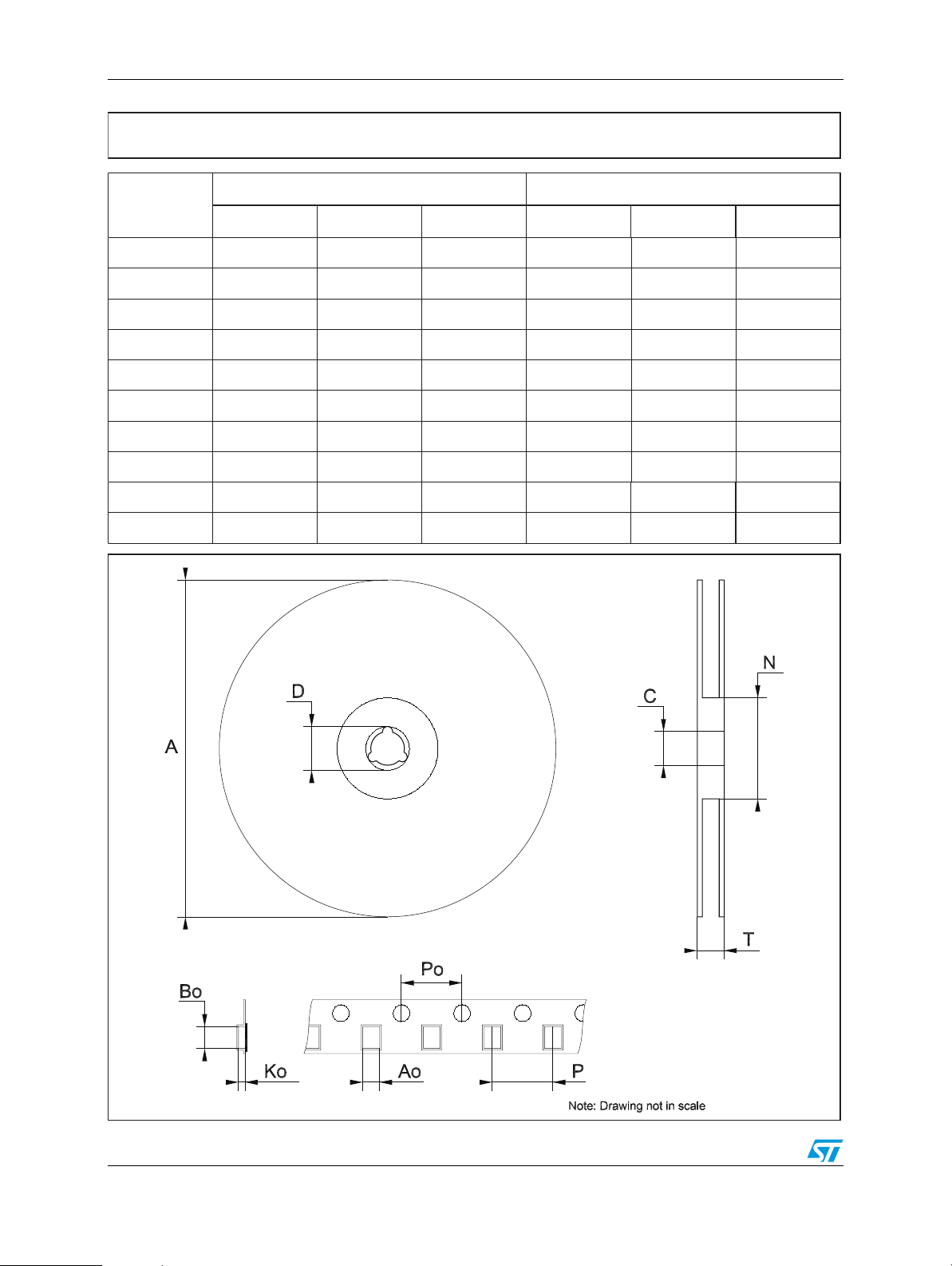
Tape and reel QFNxx/DFNxx (5x6 mm) mechanical data
mm. inch.
Dim.
Min. Typ. Max. Min. Typ. Max.
A 330 12.992
C 12.8 13.2 0.504 0.520
D 20.2 0.795
N 99 101 3.898 3.976
T 14.4 0.567
Ao 5.30 0.209
Bo 6.30 0.248
Ko 1.20 0.047
Po 4 0.157
P 8 0.315
26/29
Page 27
ST2L05-3300 Different output voltage versions of the ST2L05-3300 available on request
9 Different output voltage versions of the ST2L05-3300
available on request
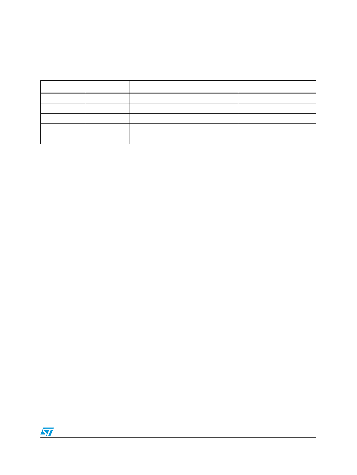
Table 14. Options available on request
V
O1
1.8 V ADJ ST2L05R1800PS Tape and reel
2.5 V ADJ ST2L05R2500PS Tape and reel
2.8 V ADJ ST2L05R2800PS Tape and reel
3.0 V 1.5 V ST2L05R3015PS Tape and reel
3.0 V ADJ ST2L05R3000PS Tape and reel
V
O2
Order codes Shipment
27/29
Page 28
Revision history ST2L05-3300
10 Revision history
Table 15. Document revision history
Date Revision Changes
18-Nov-2004 4 Removed PPAK version.
24-Nov-2004 5 Added new mechanical data.
06-Dec-2004 6 Modified mechanical data.
13-Feb-2009 7 Removed SPAK5-L version.
28/29
Page 29

ST2L05-3300
Please Read Carefully:
Information in this document is provided solely in connection with ST products. STMicroelectronics NV and its subsidiaries (“ST”) reserve the
right to make changes, corrections, modifications or improvements, to this document, and the products and services described herein at any
time, without notice.
All ST products are sold pursuant to ST’s terms and conditions of sale.
Purchasers are solely responsible for the choice, selection and use of the ST products and services described herein, and ST assumes no
liability whatsoever relating to the choice, selection or use of the ST products and services described herein.
No license, express or implied, by estoppel or otherwise, to any intellectual property rights is granted under this document. If any part of this
document refers to any third party products or services it shall not be deemed a license grant by ST for the use of such third party products
or services, or any intellectual property contained therein or considered as a warranty covering the use in any manner whatsoever of such
third party products or services or any intellectual property contained therein.
UNLESS OTHERWISE SET FORTH IN ST’S TERMS AND CONDITIONS OF SALE ST DISCLAIMS ANY EXPRESS OR IMPLIED
WARRANTY WITH RESPECT TO THE USE AND/OR SALE OF ST PRODUCTS INCLUDING WITHOUT LIMITATION IMPLIED
WARRANTIES OF MERCHANTABILITY, FITNESS FOR A PARTICULAR PURPOSE (AND THEIR EQUIVALENTS UNDER THE LAWS
OF ANY JURISDICTION), OR INFRINGEMENT OF ANY PATENT, COPYRIGHT OR OTHER INTELLECTUAL PROPERTY RIGHT.
UNLESS EXPRESSLY APPROVED IN WRITING BY AN AUTHORIZED ST REPRESENTATIVE, ST PRODUCTS ARE NOT
RECOMMENDED, AUTHORIZED OR WARRANTED FOR USE IN MILITARY, AIR CRAFT, SPACE, LIFE SAVING, OR LIFE SUSTAINING
APPLICATIONS, NOR IN PRODUCTS OR SYSTEMS WHERE FAILURE OR MALFUNCTION MAY RESULT IN PERSONAL INJURY,
DEATH, OR SEVERE PROPERTY OR ENVIRONMENTAL DAMAGE. ST PRODUCTS WHICH ARE NOT SPECIFIED AS "AUTOMOTIVE
GRADE" MAY ONLY BE USED IN AUTOMOTIVE APPLICATIONS AT USER’S OWN RISK.
Resale of ST products with provisions different from the statements and/or technical features set forth in this document shall immediately void
any warranty granted by ST for the ST product or service described herein and shall not create or extend in any manner whatsoever, any
liability of ST.
ST and the ST logo are trademarks or registered trademarks of ST in various countries.
Information in this document supersedes and replaces all information previously supplied.
The ST logo is a registered trademark of STMicroelectronics. All other names are the property of their respective owners.
© 2009 STMicroelectronics - All rights reserved
STMicroelectronics group of companies
Australia - Belgium - Brazil - Canada - China - Czech Republic - Finland - France - Germany - Hong Kong - India - Israel - Italy - Japan -
Malaysia - Malta - Morocco - Singapore - Spain - Sweden - Switzerland - United Kingdom - United States of America
www.st.com
29/29
 Loading...