

13.56 MHz short-range contactless memory chip
–Unsawn wafer
– Bumped and sawn wafer
with 512-bit EEPROM and anticollision functions
Features
■ ISO 14443-2 Type B air interface compliant
■ ISO 14443-3 Type B frame format compliant
■ 13.56 MHz carrier frequency
■ 847 kHz subcarrier frequency
■ 106 Kbit/second data transfer
■ 8 bit Chip_ID based anticollision system
■ 2 Count-down binary counters with automated
antitearing protection
■ 64-bit Unique Identifier
■ 512-bit EEPROM with write protect feature
■ Read_block and Write_block (32 bits)
■ Internal tuning capacitor
■ 1million erase/write cycles
■ 40-year data retention
■ Self-timed programming cycle
■ 5 ms typical programming time
SRI512
September 2011 Doc ID 13263 Rev 6 1/47
www.st.com
1

Contents SRI512
Contents
1 Description . . . . . . . . . . . . . . . . . . . . . . . . . . . . . . . . . . . . . . . . . . . . . . . . . 7
2 Signal description . . . . . . . . . . . . . . . . . . . . . . . . . . . . . . . . . . . . . . . . . . . 8
2.1 AC1, AC0 . . . . . . . . . . . . . . . . . . . . . . . . . . . . . . . . . . . . . . . . . . . . . . . . . . 8
3 Data transfer . . . . . . . . . . . . . . . . . . . . . . . . . . . . . . . . . . . . . . . . . . . . . . . 9
3.1 Input data transfer from the reader to the SRI512 (request frame) . . . . . . 9
3.1.1 Character transmission format for request frame . . . . . . . . . . . . . . . . . . 9
3.1.2 Request start of frame . . . . . . . . . . . . . . . . . . . . . . . . . . . . . . . . . . . . . . 10
3.1.3 Request end of frame . . . . . . . . . . . . . . . . . . . . . . . . . . . . . . . . . . . . . . 10
3.2 Output data transfer from the SRI512 to the reader (answer frame) . . . . 11
3.2.1 Character transmission format for answer frame . . . . . . . . . . . . . . . . . . 11
3.2.2 Answer start of frame . . . . . . . . . . . . . . . . . . . . . . . . . . . . . . . . . . . . . . . 11
3.2.3 Answer end of frame . . . . . . . . . . . . . . . . . . . . . . . . . . . . . . . . . . . . . . . 12
3.3 Transmission frame . . . . . . . . . . . . . . . . . . . . . . . . . . . . . . . . . . . . . . . . . 12
3.4 CRC . . . . . . . . . . . . . . . . . . . . . . . . . . . . . . . . . . . . . . . . . . . . . . . . . . . . . 13
4 Memory mapping . . . . . . . . . . . . . . . . . . . . . . . . . . . . . . . . . . . . . . . . . . 14
4.1 Resettable OTP area . . . . . . . . . . . . . . . . . . . . . . . . . . . . . . . . . . . . . . . . 15
4.2 32-bit binary counters . . . . . . . . . . . . . . . . . . . . . . . . . . . . . . . . . . . . . . . . 16
4.3 EEPROM area . . . . . . . . . . . . . . . . . . . . . . . . . . . . . . . . . . . . . . . . . . . . . 18
4.4 System area . . . . . . . . . . . . . . . . . . . . . . . . . . . . . . . . . . . . . . . . . . . . . . . 19
4.4.1 OTP_Lock_Reg . . . . . . . . . . . . . . . . . . . . . . . . . . . . . . . . . . . . . . . . . . . 19
4.4.2 Fixed Chip_ID (option) . . . . . . . . . . . . . . . . . . . . . . . . . . . . . . . . . . . . . . 20
5 SRI512 operation . . . . . . . . . . . . . . . . . . . . . . . . . . . . . . . . . . . . . . . . . . . 21
6 SRI512 states . . . . . . . . . . . . . . . . . . . . . . . . . . . . . . . . . . . . . . . . . . . . . . 22
6.1 Power-off state . . . . . . . . . . . . . . . . . . . . . . . . . . . . . . . . . . . . . . . . . . . . . 22
6.2 Ready state . . . . . . . . . . . . . . . . . . . . . . . . . . . . . . . . . . . . . . . . . . . . . . . 22
6.3 Inventory state . . . . . . . . . . . . . . . . . . . . . . . . . . . . . . . . . . . . . . . . . . . . . 22
6.4 Selected state . . . . . . . . . . . . . . . . . . . . . . . . . . . . . . . . . . . . . . . . . . . . . 22
6.5 Deselected state . . . . . . . . . . . . . . . . . . . . . . . . . . . . . . . . . . . . . . . . . . . . 22
2/47 Doc ID 13263 Rev 6

SRI512 Contents
6.6 Deactivated state . . . . . . . . . . . . . . . . . . . . . . . . . . . . . . . . . . . . . . . . . . . 22
7 Anticollision . . . . . . . . . . . . . . . . . . . . . . . . . . . . . . . . . . . . . . . . . . . . . . . 24
7.1 Description of an anticollision sequence . . . . . . . . . . . . . . . . . . . . . . . . . 26
8 SRI512 commands . . . . . . . . . . . . . . . . . . . . . . . . . . . . . . . . . . . . . . . . . 28
8.1 Initiate() command . . . . . . . . . . . . . . . . . . . . . . . . . . . . . . . . . . . . . . . . . . 29
8.2 Pcall16() command . . . . . . . . . . . . . . . . . . . . . . . . . . . . . . . . . . . . . . . . . 30
8.3 Slot_marker(SN) command . . . . . . . . . . . . . . . . . . . . . . . . . . . . . . . . . . . 31
8.4 Select(Chip_ID) command . . . . . . . . . . . . . . . . . . . . . . . . . . . . . . . . . . . . 32
8.5 Completion() command . . . . . . . . . . . . . . . . . . . . . . . . . . . . . . . . . . . . . . 33
8.6 Reset_to_inventory() command . . . . . . . . . . . . . . . . . . . . . . . . . . . . . . . . 34
8.7 Read_block(Addr) command . . . . . . . . . . . . . . . . . . . . . . . . . . . . . . . . . . 35
8.8 Write_block (Addr, Data) command . . . . . . . . . . . . . . . . . . . . . . . . . . . . . 36
8.9 Get_UID() command . . . . . . . . . . . . . . . . . . . . . . . . . . . . . . . . . . . . . . . . 37
8.10 Power-on state . . . . . . . . . . . . . . . . . . . . . . . . . . . . . . . . . . . . . . . . . . . . . 38
9 Maximum rating . . . . . . . . . . . . . . . . . . . . . . . . . . . . . . . . . . . . . . . . . . . . 39
10 DC and AC parameters . . . . . . . . . . . . . . . . . . . . . . . . . . . . . . . . . . . . . . 40
11 Part numbering . . . . . . . . . . . . . . . . . . . . . . . . . . . . . . . . . . . . . . . . . . . . 42
Appendix A ISO 14443 Type B CRC calculation . . . . . . . . . . . . . . . . . . . . . . . . . 43
Appendix B SRI512 command brief . . . . . . . . . . . . . . . . . . . . . . . . . . . . . . . . . . . 44
Revision history . . . . . . . . . . . . . . . . . . . . . . . . . . . . . . . . . . . . . . . . . . . . . . . . . . . . 46
Doc ID 13263 Rev 6 3/47

List of tables SRI512
List of tables
Table 1. Signal names . . . . . . . . . . . . . . . . . . . . . . . . . . . . . . . . . . . . . . . . . . . . . . . . . . . . . . . . . . . . 7
Table 2. Bit description . . . . . . . . . . . . . . . . . . . . . . . . . . . . . . . . . . . . . . . . . . . . . . . . . . . . . . . . . . . 10
Table 3. SRI512 memory mapping . . . . . . . . . . . . . . . . . . . . . . . . . . . . . . . . . . . . . . . . . . . . . . . . . . 14
Table 4. Standard anticollision sequence . . . . . . . . . . . . . . . . . . . . . . . . . . . . . . . . . . . . . . . . . . . . . 26
Table 5. Command code . . . . . . . . . . . . . . . . . . . . . . . . . . . . . . . . . . . . . . . . . . . . . . . . . . . . . . . . . 28
Table 6. Absolute maximum ratings . . . . . . . . . . . . . . . . . . . . . . . . . . . . . . . . . . . . . . . . . . . . . . . . . 39
Table 7. Operating conditions. . . . . . . . . . . . . . . . . . . . . . . . . . . . . . . . . . . . . . . . . . . . . . . . . . . . . . 40
Table 8. DC characteristics. . . . . . . . . . . . . . . . . . . . . . . . . . . . . . . . . . . . . . . . . . . . . . . . . . . . . . . . 40
Table 9. AC characteristics. . . . . . . . . . . . . . . . . . . . . . . . . . . . . . . . . . . . . . . . . . . . . . . . . . . . . . . . 40
Table 10. Ordering information scheme . . . . . . . . . . . . . . . . . . . . . . . . . . . . . . . . . . . . . . . . . . . . . . . 42
Table 11. Document revision history . . . . . . . . . . . . . . . . . . . . . . . . . . . . . . . . . . . . . . . . . . . . . . . . . 46
4/47 Doc ID 13263 Rev 6

SRI512 List of figures
List of figures
Figure 1. Logic diagram . . . . . . . . . . . . . . . . . . . . . . . . . . . . . . . . . . . . . . . . . . . . . . . . . . . . . . . . . . . . 7
Figure 2. Die floor plan. . . . . . . . . . . . . . . . . . . . . . . . . . . . . . . . . . . . . . . . . . . . . . . . . . . . . . . . . . . . . 8
Figure 3. 10% ASK modulation of the received wave . . . . . . . . . . . . . . . . . . . . . . . . . . . . . . . . . . . . . 9
Figure 4. SRI512 request frame character format . . . . . . . . . . . . . . . . . . . . . . . . . . . . . . . . . . . . . . . . 9
Figure 5. Request start of frame . . . . . . . . . . . . . . . . . . . . . . . . . . . . . . . . . . . . . . . . . . . . . . . . . . . . 10
Figure 6. Request end of frame . . . . . . . . . . . . . . . . . . . . . . . . . . . . . . . . . . . . . . . . . . . . . . . . . . . . . 10
Figure 7. Wave transmitted using BPSK subcarrier modulation . . . . . . . . . . . . . . . . . . . . . . . . . . . . 11
Figure 8. Answer start of frame . . . . . . . . . . . . . . . . . . . . . . . . . . . . . . . . . . . . . . . . . . . . . . . . . . . . . 11
Figure 9. Answer end of frame. . . . . . . . . . . . . . . . . . . . . . . . . . . . . . . . . . . . . . . . . . . . . . . . . . . . . . 12
Figure 10. Example of a complete transmission frame . . . . . . . . . . . . . . . . . . . . . . . . . . . . . . . . . . . . 12
Figure 11. CRC transmission rules . . . . . . . . . . . . . . . . . . . . . . . . . . . . . . . . . . . . . . . . . . . . . . . . . . . 13
Figure 12. Resettable OTP area (addresses 0 to 4) . . . . . . . . . . . . . . . . . . . . . . . . . . . . . . . . . . . . . . 15
Figure 13. Write_block update in standard mode (binary format) . . . . . . . . . . . . . . . . . . . . . . . . . . . . 15
Figure 14. Write_block update in reload mode (binary format) . . . . . . . . . . . . . . . . . . . . . . . . . . . . . . 16
Figure 15. Binary counter (addresses 5 to 6). . . . . . . . . . . . . . . . . . . . . . . . . . . . . . . . . . . . . . . . . . . . 16
Figure 16. Count down example (binary format) . . . . . . . . . . . . . . . . . . . . . . . . . . . . . . . . . . . . . . . . . 17
Figure 17. EEPROM (addresses 7 to 15) . . . . . . . . . . . . . . . . . . . . . . . . . . . . . . . . . . . . . . . . . . . . . . 18
Figure 18. System area . . . . . . . . . . . . . . . . . . . . . . . . . . . . . . . . . . . . . . . . . . . . . . . . . . . . . . . . . . . . 19
Figure 19. State transition diagram . . . . . . . . . . . . . . . . . . . . . . . . . . . . . . . . . . . . . . . . . . . . . . . . . . . 23
Figure 20. SRI512 Chip_ID description . . . . . . . . . . . . . . . . . . . . . . . . . . . . . . . . . . . . . . . . . . . . . . . . 24
Figure 21. Description of a possible anticollision sequence . . . . . . . . . . . . . . . . . . . . . . . . . . . . . . . . 25
Figure 22. Example of an anticollision sequence. . . . . . . . . . . . . . . . . . . . . . . . . . . . . . . . . . . . . . . . . 27
Figure 23. Initiate request format . . . . . . . . . . . . . . . . . . . . . . . . . . . . . . . . . . . . . . . . . . . . . . . . . . . . . 29
Figure 24. Initiate response format . . . . . . . . . . . . . . . . . . . . . . . . . . . . . . . . . . . . . . . . . . . . . . . . . . . 29
Figure 25. Initiate frame exchange between reader and SRI512 . . . . . . . . . . . . . . . . . . . . . . . . . . . . 29
Figure 26. Pcall16 request format . . . . . . . . . . . . . . . . . . . . . . . . . . . . . . . . . . . . . . . . . . . . . . . . . . . . 30
Figure 27. Pcall16 response format . . . . . . . . . . . . . . . . . . . . . . . . . . . . . . . . . . . . . . . . . . . . . . . . . . . 30
Figure 28. Pcall16 frame exchange between reader and SRI512 . . . . . . . . . . . . . . . . . . . . . . . . . . . . 30
Figure 29. Slot_marker request format . . . . . . . . . . . . . . . . . . . . . . . . . . . . . . . . . . . . . . . . . . . . . . . . 31
Figure 30. Slot_marker response format . . . . . . . . . . . . . . . . . . . . . . . . . . . . . . . . . . . . . . . . . . . . . . . 31
Figure 31. Slot_marker frame exchange between reader and SRI512 . . . . . . . . . . . . . . . . . . . . . . . . 31
Figure 32. Select request format . . . . . . . . . . . . . . . . . . . . . . . . . . . . . . . . . . . . . . . . . . . . . . . . . . . . . 32
Figure 33. Select response format . . . . . . . . . . . . . . . . . . . . . . . . . . . . . . . . . . . . . . . . . . . . . . . . . . . . 32
Figure 34. Select frame exchange between reader and SRI512 . . . . . . . . . . . . . . . . . . . . . . . . . . . . . 32
Figure 35. Completion request format . . . . . . . . . . . . . . . . . . . . . . . . . . . . . . . . . . . . . . . . . . . . . . . . . 33
Figure 36. Completion response format. . . . . . . . . . . . . . . . . . . . . . . . . . . . . . . . . . . . . . . . . . . . . . . . 33
Figure 37. Completion frame exchange between reader and SRI512. . . . . . . . . . . . . . . . . . . . . . . . . 33
Figure 38. Reset_to_inventory request format. . . . . . . . . . . . . . . . . . . . . . . . . . . . . . . . . . . . . . . . . . . 34
Figure 39. Reset_to_inventory response format . . . . . . . . . . . . . . . . . . . . . . . . . . . . . . . . . . . . . . . . . 34
Figure 40. Reset_to_inventory frame exchange between reader and SRI512 . . . . . . . . . . . . . . . . . . 34
Figure 41. Read_block request format. . . . . . . . . . . . . . . . . . . . . . . . . . . . . . . . . . . . . . . . . . . . . . . . . 35
Figure 42. Read_block response format . . . . . . . . . . . . . . . . . . . . . . . . . . . . . . . . . . . . . . . . . . . . . . . 35
Figure 43. Read_block frame exchange between reader and SRI512 . . . . . . . . . . . . . . . . . . . . . . . . 35
Figure 44. Write_block request format . . . . . . . . . . . . . . . . . . . . . . . . . . . . . . . . . . . . . . . . . . . . . . . . . 36
Figure 45. Write_block response format . . . . . . . . . . . . . . . . . . . . . . . . . . . . . . . . . . . . . . . . . . . . . . . 36
Figure 46. Write_block frame exchange between reader and SRI512 . . . . . . . . . . . . . . . . . . . . . . . . 37
Figure 47. Get_UID request format . . . . . . . . . . . . . . . . . . . . . . . . . . . . . . . . . . . . . . . . . . . . . . . . . . . 37
Figure 48. Get_UID response format . . . . . . . . . . . . . . . . . . . . . . . . . . . . . . . . . . . . . . . . . . . . . . . . . . 37
Doc ID 13263 Rev 6 5/47

List of figures SRI512
Figure 49. 64-bit unique identifier of the SRI512 . . . . . . . . . . . . . . . . . . . . . . . . . . . . . . . . . . . . . . . . . 38
Figure 50. Get_UID frame exchange between reader and SRI512 . . . . . . . . . . . . . . . . . . . . . . . . . . . 38
Figure 51. SRI512 synchronous timing, transmit and receive . . . . . . . . . . . . . . . . . . . . . . . . . . . . . . . 41
Figure 52. Initiate frame exchange between reader and SRI512 . . . . . . . . . . . . . . . . . . . . . . . . . . . . 44
Figure 53. Pcall16 frame exchange between reader and SRI512 . . . . . . . . . . . . . . . . . . . . . . . . . . . . 44
Figure 54. Slot_marker frame exchange between reader and SRI512 . . . . . . . . . . . . . . . . . . . . . . . . 44
Figure 55. Select frame exchange between reader and SRI512 . . . . . . . . . . . . . . . . . . . . . . . . . . . . . 44
Figure 56. Completion frame exchange between reader and SRI512. . . . . . . . . . . . . . . . . . . . . . . . . 44
Figure 57. Reset_to_inventory frame exchange between reader and SRI512 . . . . . . . . . . . . . . . . . . 45
Figure 58. Read_block frame exchange between reader and SRI512 . . . . . . . . . . . . . . . . . . . . . . . . 45
Figure 59. Write_block frame exchange between reader and SRI512 . . . . . . . . . . . . . . . . . . . . . . . . 45
Figure 60. Get_UID frame exchange between reader and SRI512 . . . . . . . . . . . . . . . . . . . . . . . . . . . 45
6/47 Doc ID 13263 Rev 6
SRI512 Description
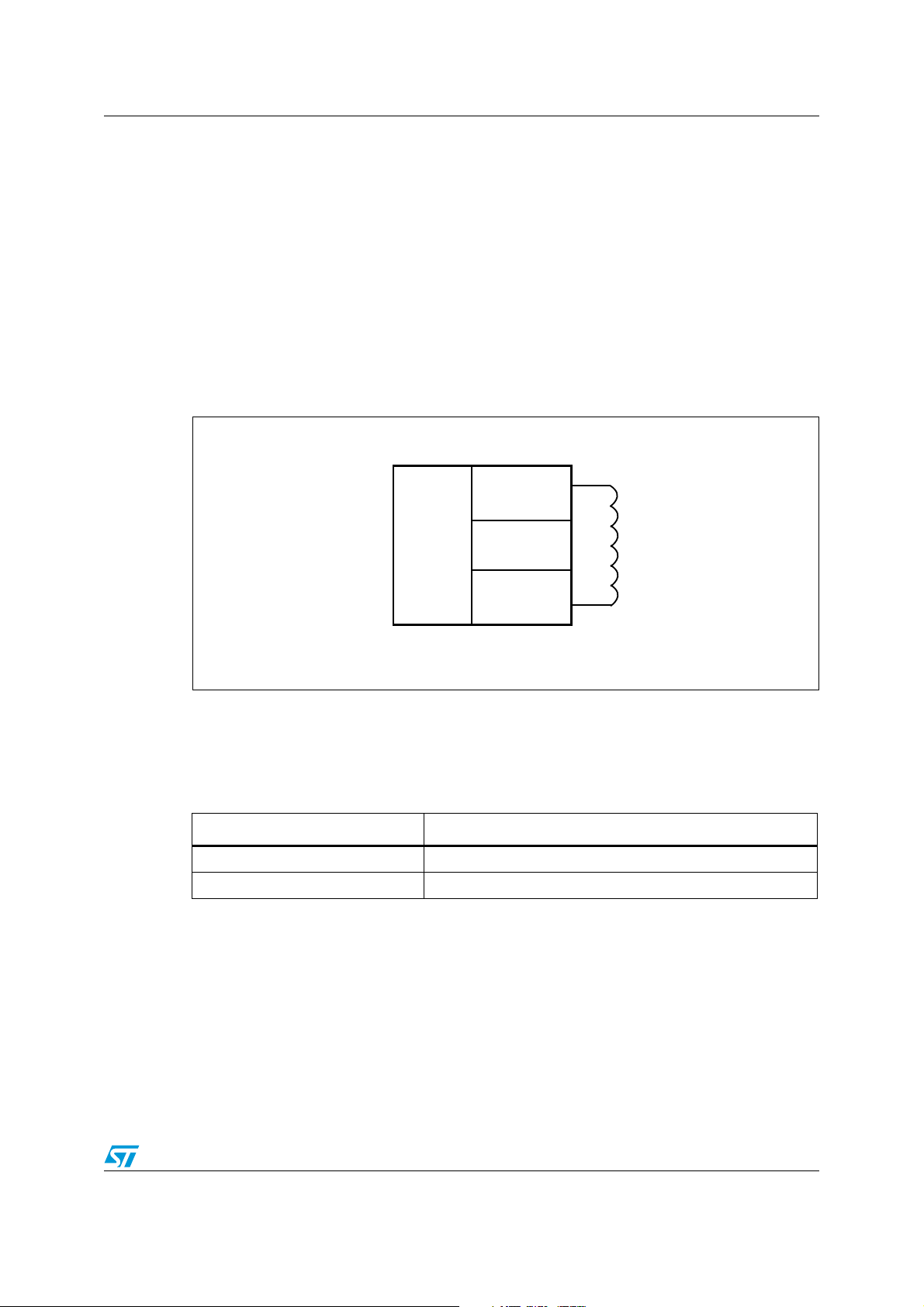
AI10795
AC1
SRI512
AC0
Power
Supply
Regulator
BPSK
Load
Modulator
ASK
Demodulator
512-bit
User
EEPROM
1 Description
The SRI512 is a contactless memory, powered by an externally transmitted radio wave. It
contains a 512-bit user EEPROM. The memory is organized as 16 blocks of 32 bits. The
SRI512 is accessed via the 13.56 MHz carrier. Incoming data are demodulated and
decoded from the received amplitude shift keying (ASK) modulation signal and outgoing
data are generated by load variation using bit phase shift keying (BPSK) coding of a
847 kHz subcarrier. The received ASK wave is 10% modulated. The data transfer rate
between the SRI512 and the reader is 106 Kbit/s in both reception and emission modes.
The SRI512 follows the ISO 14443-2 Type B recommendation for the radio-frequency power
and signal interface.
Figure 1. Logic diagram
The SRI512 is specifically designed for short range applications that need re-usable
products. The SRI512 includes an anticollision mechanism that allows it to detect and select
tags present at the same time within range of the reader. Using the STMicroelectronics
single chip coupler, CRX14, it is easy to design a reader and build a contactless system.
Table 1. Signal names
AC1 Antenna coil
AC0 Antenna coil
Signal name Description
Doc ID 13263 Rev 6 7/47

Signal description SRI512
AI09055
AC1AC0
The SRI512 contactless EEPROM can be randomly read and written in block mode (each
block containing 32 bits). The instruction set includes the following nine commands:
● Read_block
● Write_block
● Initiate
● Pcall16
● Slot_marker
● Select
● Completion
● Reset_to_inventory
● Get_UID
The SRI512 memory is organized in three areas, as described in Tab l e 3 . The first area is a
resettable OTP (one-time programmable) area in which bits can only be switched from 1 to
0. Using a special command, it is possible to erase all bits of this area to 1.
The second area provides two 32-bit binary counters that can only be decremented from
FFFF FFFFh to 0000 0000h, and gives a capacity of 4,294,967,296 units per counter.
The last area is the EEPROM memory. It is accessible by block of 32 bits and includes an
auto-erase cycle during each Write_block command.
Figure 2. Die floor plan
2 Signal description
2.1 AC1, AC0
The pads for the Antenna Coil. AC1 and AC0 must be directly bonded to the antenna.
8/47 Doc ID 13263 Rev 6

SRI512 Data transfer
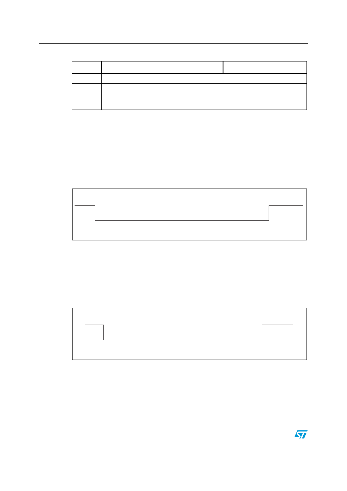
DATA BIT TO TRANSMIT
TO THE
10% ASK MODULATION
OF THE 13.56MHz WAVE,
GENERATED BY THE READER
Transfer time for one data bit is 1/106 kHz
SRI512
Ai10796
ai07664
1 ETU
Start
"0"
Stop
"1"
MSbLSb Information Byte
b0 b1 b2 b3 b4 b5 b6 b7 b8 b9
3 Data transfer
3.1 Input data transfer from the reader to the SRI512 (request frame)
The reader must generate a 13.56 MHz sinusoidal carrier frequency at its antenna, with
enough energy to “remote-power” the memory. The energy received at the SRI512’s
antenna is transformed into a supply voltage by a regulator, and into data bits by the ASK
demodulator. For the SRI512 to decode correctly the information it receives, the reader must
10% amplitude-modulate the 13.56 MHz wave before sending it to the SRI512. This is
represented in Figure 3. The data transfer rate is 106 Kbits/s.
Figure 3. 10% ASK modulation of the received wave
3.1.1 Character transmission format for request frame
The SRI512 transmits and receives data bytes as 10-bit characters, with the least significant
bit (b
) transmitted first, as shown in Figure 4. Each bit duration, an ETU (elementary time
0
unit), is equal to 9.44 µs (1/106 kHz).
These characters, framed by a start of frame (SOF) and an end of frame (EOF), are put
together to form a command frame as shown in Figure 10. A frame includes an SOF,
commands, addresses, data, a CRC and an EOF as defined in the ISO 14443-3 Type B
Standard. If an error is detected during data transfer, the SRI512 does not execute the
command, but it does not generate an error frame.
Figure 4. SRI512 request frame character format
Doc ID 13263 Rev 6 9/47
Data transfer SRI512
ai07665
ETU
b0 b1 b2 b3 b4 b5 b6 b7 b8 b9 b10 b11
000000000011
ai07666
ETU
b0 b1 b2 b3 b4 b5 b6 b7 b8 b9
0000000000
Table 2. Bit description
Bit Description Value
b
Start bit used to synchronize the transmission b0 = 0
0
b1 to b8Information byte (command, address or data)
b
Stop bit used to indicate the end of a character b9 = 1
9
3.1.2 Request start of frame
The SOF described in Figure 5 is composed of:
● one falling edge,
● followed by 10 ETUs at logic-0,
● followed by a single rising edge,
● followed by at least 2 ETUs (and at most 3) at logic-1.
Figure 5. Request start of frame
The information byte is sent with
the least significant bit first
3.1.3 Request end of frame
The EOF shown in Figure 6 is composed of:
● one falling edge,
● followed by 10 ETUs at logic-0,
● followed by a single rising edge.
Figure 6. Request end of frame
10/47 Doc ID 13263 Rev 6
SRI512 Data transfer
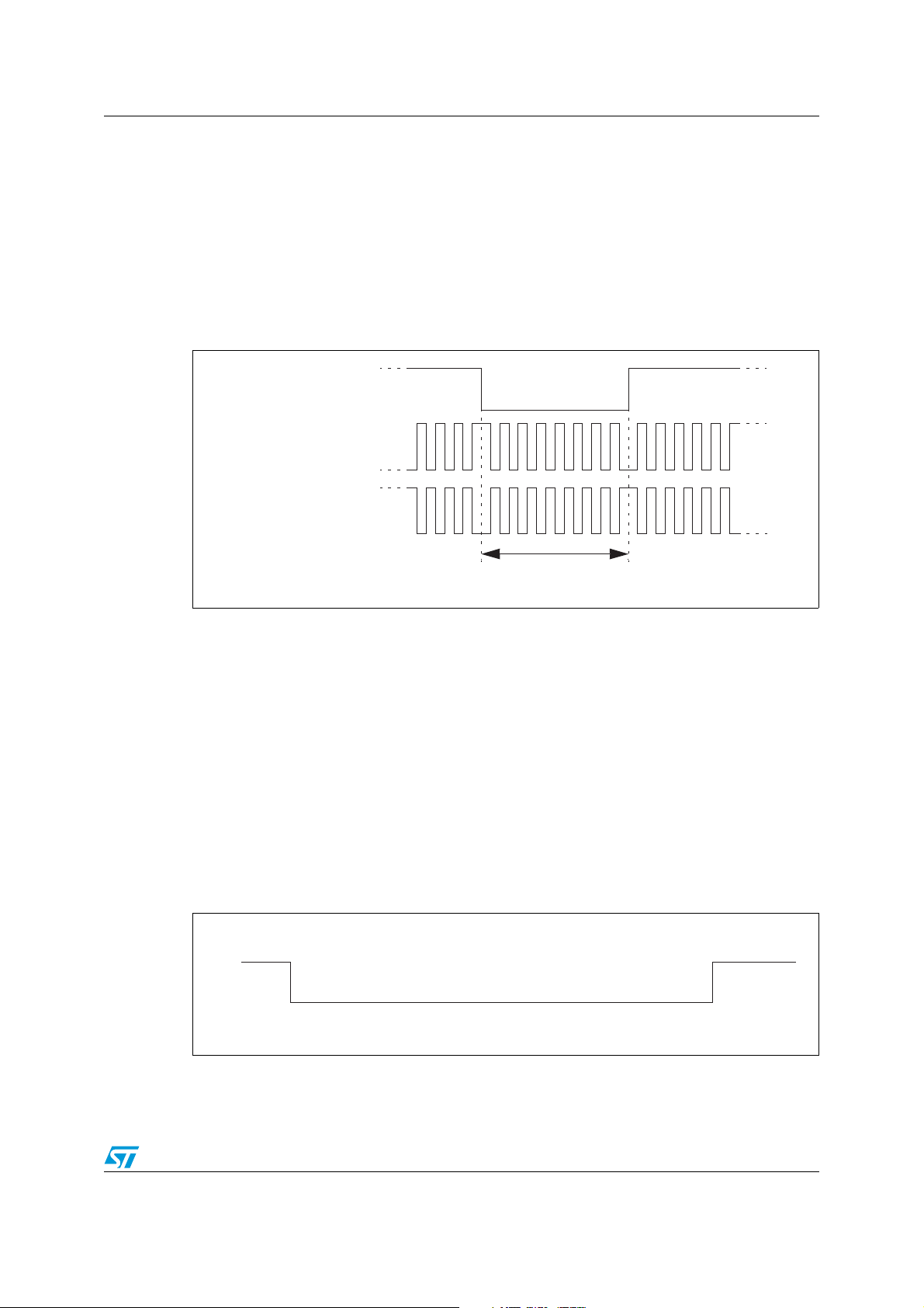
Or
AI10797
Data Bit to be Transmitted
to the Reader
847kHz BPSK Modulation
Generated by the SRI512
BPSK Modulation at 847kHz
During a One-bit Data Transfer Time (1/106kHz)
ai07665
ETU
b0 b1 b2 b3 b4 b5 b6 b7 b8 b9 b10 b11
000000000011
3.2 Output data transfer from the SRI512 to the reader (answer frame)
The data bits issued by the SRI512 use back-scattering. Back-scattering is obtained by
modifying the SRI512 current consumption at the antenna (load modulation). The load
modulation causes a variation at the reader antenna by inductive coupling. With appropriate
detector circuitry, the reader is able to pick up information from the SRI512. To improve loadmodulation detection, data is transmitted using a BPSK encoded, 847 kHz subcarrier
frequency ƒ
Figure 7. Wave transmitted using BPSK subcarrier modulation
as shown in Figure 7, and as specified in the ISO 14443-2 Type B Standard.
s
3.2.1 Character transmission format for answer frame
3.2.2 Answer start of frame
The character format is the same as for input data transfer (Figure 4). The transmitted
frames are made up of an SOF, data, a CRC and an EOF (Figure 10). As with an input data
transfer, if an error occurs, the reader does not issue an error code to the SRI512, but it
should be able to detect it and manage the situation. The data transfer rate is
106 Kbits/second.
The SOF described in Figure 8 is composed of:
● followed by 10 ETUs at logic-0
● followed by 2 ETUs at logic-1
Figure 8. Answer start of frame
Doc ID 13263 Rev 6 11/47

Data transfer SRI512
ai07665
ETU
b0 b1 b2 b3 b4 b5 b6 b7 b8 b9 b10 b11
000000000011
12 bits
10 bits
Sync
128/fs
128/fs
fs=847.5kHz
t
DR
t
0
t
1
SOF
Cmd
Data CRC CRC
EOF
10 bits 10 bits 10 bits 10 bits
12 bits
10 bits 10 bits 10 bits
Data CRC CRC
SOF
EOF
12 bits
SOF
t
2
Ai10798
Input data transfer using ASK Output data transfer using BPSK
Sent by the
Reader
Sent by the
SRI512
at 106kb/s
3.2.3 Answer end of frame
The EOF shown in Figure 9 is composed of:
● followed by 10 ETUs at logic-0,
● followed by 2 ETUs at logic-1.
Figure 9. Answer end of frame
3.3 Transmission frame
Between the request data transfer and the answer data transfer, all ASK and BPSK
modulations are suspended for a minimum time of t
to switch from Transmission to Reception mode. It is repeated after each frame. After t
13.56 MHz carrier frequency is modulated by the SRI512 at 847 kHz for a period of
t
=128/ƒS to allow the reader to synchronize. After t1, the first phase transition generated
1
by the SRI512 forms the start bit (‘0’) of the answer SOF. After the falling edge of the answer
EOF, the reader waits a minimum time, t
, before sending a new request frame to the
2
SRI512.
= 128/ƒS. This delay allows the reader
0
, the
0
Figure 10. Example of a complete transmission frame
12/47 Doc ID 13263 Rev 6

SRI512 Data transfer
CRC 16 (8 bits) CRC 16 (8 bits)
LSbit MSbit LSbit MSbit
LSByte MSByte
ai07667
3.4 CRC
The 16-bit CRC used by the SRI512 is generated in compliance with the ISO14443 Type B
recommendation. For further information, please see Appendix A. The initial register
contents are all 1’s: FFFFh.
The two-byte CRC is present in every request and in every answer frame, before the EOF.
The CRC is calculated on all the bytes between SOF (not included) and the CRC field.
Upon reception of a request from a reader, the SRI512 verifies that the CRC value is valid. If
it is invalid, the SRI512 discards the frame and does not answer the reader.
Upon reception of an answer from the SRI512, the reader should verify the validity of the
CRC. In case of error, the actions to be taken are the reader designer’s responsibility.
The CRC is transmitted with the least significant byte first and each byte is transmitted with
the least significant bit first.
Figure 11. CRC transmission rules
Doc ID 13263 Rev 6 13/47

Memory mapping SRI512
4 Memory mapping
The SRI512 is organized as 16 blocks of 32 bits as shown in Ta bl e 3 . All blocks are
accessible by the Read_block command. Depending on the write access, they can be
updated by the Write_block command. A Write_block updates all the 32 bits of the block.
Table 3. SRI512 memory mapping
Block
Addr
0 32 bits Boolean area
1 32 bits Boolean area
2 32 bits Boolean area
3 32 bits Boolean area
4 32 bits Boolean area
Msb 32-bit block Lsb
b
31
b16b15b
14
b8 b
7
Description
b
0
Resettable OTP
bits
5 32 bits binary counter
6 32 bits binary counter
7User area
8User area
9User area
10 User area
11 User area
12 User area
13 User area
14 User area
15 User area
255 OTP_Lock_Reg 0 ST Reserved
Fixed Chip_ID
(Option)
UID0
64 bits UID area ROM
UID1
Count down
Counter
Lockable
EEPROM
System OTP bits
14/47 Doc ID 13263 Rev 6

SRI512 Memory mapping
Block
Address
MSb
b31
32-bit Block
b16 b15 b14 b8 b7
LSb
b0
Description
Resettable
OTP Bit
0
1
2
3
4
32-bit Boolean Area
32-bit Boolean Area
32-bit Boolean Area
32-bit Boolean Area
32-bit Boolean Area
ai12381
ai07658
1 ... 1 1 01011111 0 11
1 ... 1 0 01011001 1 11
1 ... 1 0 01011001 0 11
Previous data stored in block
Data to be written
New data stored in block
b31 b0
4.1 Resettable OTP area
This area contains five individual 32-bit Boolean words (see Figure 12 for a map of the
area). A Write_block command will not erase the previous contents of the block as the write
cycle is not preceded by an auto-erase cycle. This feature can be used to reset selected bits
from 1 to 0. All bits previously at 0 remain unchanged. When the 32 bits of a block are all at
0, the block is empty, and cannot be updated any more. See Figure 13 and Figure 14 for
examples of the result of the Write_block command in the resettable OTP area.
Figure 12. Resettable OTP area (addresses 0 to 4)
Figure 13. Write_block update in standard mode (binary format)
The five 32-bit blocks making up the Resettable OTP area can be erased in one go by
adding an auto-erase cycle to the Write_block command. An auto-erase cycle is added
each time the SRI512 detects a Reload command. The Reload command is implemented
through a specific update of the 32-bit binary counter located at block address 6 (see
Section 4.2: 32-bit binary counters for details).
Doc ID 13263 Rev 6 15/47
 Loading...