

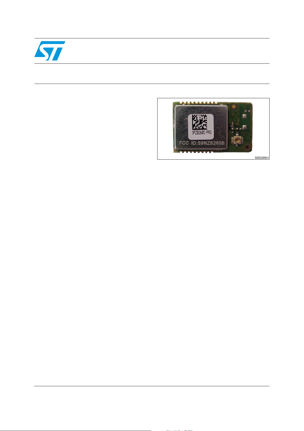
Low-power, compact ZigBee® module
Features
■ Integrated 2.4 GHz, IEEE 802.15.4 compliant
transceiver:
– + 3 dBm nominal TX output power (at UFL
connector level)
– + 5 dBm in boost mode
– -95 dBm (typ) RX sensitivity
– RX filtering for co-existence with IEEE
802.11g and Bluetooth
– Integrated VCP and loop filter
■ SPI or UART interface available for connection
with a host processor
■ On-board 24 MHz stable Xtal
■ Operates in the -40 °C to +85 °C industrial
temperature range
■ 1 µA power consumption in deep sleep mode
■ Pins available for non-intrusive debug interface
(SIF)
■ Single supply voltage (2.1 V to 3.6 V)
■ Integrated RF UFL connector for external
antenna
■ CE and RoHS compliant
■ FCC compliant (FCC ID: S9NZB260B)
®
devices
SPZB260C-PRO
Description
The SPZB260C-PRO is a low power, compact
ZigBee
applications. It enables OEMs to easily add
wireless capability to electronic devices.
The module is based on the EM260 ZigBee
network processor, which integrates a 2.4 GHz
IEEE 802.15.4 compliant transceiver and IEEE
802.15.4 PHY and MAC.
A single supply voltage is required to power the
module. The voltage supply also determines the
I/O port level, allowing easy integration with the
target device. The module integrates an RF UFL
connector, allowing the use of an external
antenna.
®
module optimized for embedded
Applications
The EM260 provides an SPI-based serial
interface (EZSP - EmberZNet serial protocol) or
■ Industrial control
■ Sensor networking
■ Monitoring of remote systems
■ Home appliances
■ Security systems
■ Lighting control
■ Metering
September 2010 Doc ID 17301 Rev 1 1/15
UART interface to the EmberZNet APIs, both
accessible from the module.
The module is shipped with the EmberZnet PRO
version 3.3.1 loaded into the Flash memory for
use of the SPI-based serial interface.
For details or additional information, please refer
to the EM260 datasheet available on the Ember
Corporation website.
www.st.com
15

Contents SPZB260C-PRO
Contents
1 Block diagram . . . . . . . . . . . . . . . . . . . . . . . . . . . . . . . . . . . . . . . . . . . . . . 3
2 Pin information . . . . . . . . . . . . . . . . . . . . . . . . . . . . . . . . . . . . . . . . . . . . . 4
2.1 Pin connections . . . . . . . . . . . . . . . . . . . . . . . . . . . . . . . . . . . . . . . . . . . . . 4
2.2 Pin description . . . . . . . . . . . . . . . . . . . . . . . . . . . . . . . . . . . . . . . . . . . . . . 5
3 Maximum ratings . . . . . . . . . . . . . . . . . . . . . . . . . . . . . . . . . . . . . . . . . . . . 6
3.1 Absolute maximum ratings . . . . . . . . . . . . . . . . . . . . . . . . . . . . . . . . . . . . . 6
3.2 Operating ranges . . . . . . . . . . . . . . . . . . . . . . . . . . . . . . . . . . . . . . . . . . . . 6
4 Electrical characteristics . . . . . . . . . . . . . . . . . . . . . . . . . . . . . . . . . . . . . 7
4.1 DC electrical characteristics . . . . . . . . . . . . . . . . . . . . . . . . . . . . . . . . . . . . 7
4.2 DC I/O specifications . . . . . . . . . . . . . . . . . . . . . . . . . . . . . . . . . . . . . . . . . 7
4.3 RF electrical characteristics . . . . . . . . . . . . . . . . . . . . . . . . . . . . . . . . . . . . 8
5 Package mechanical dimensions . . . . . . . . . . . . . . . . . . . . . . . . . . . . . . 9
6 Soldering . . . . . . . . . . . . . . . . . . . . . . . . . . . . . . . . . . . . . . . . . . . . . . . . . 11
Appendix A FCC statement . . . . . . . . . . . . . . . . . . . . . . . . . . . . . . . . . . . . . . . . . . 12
A.1 Instructions for FCC ID labeling . . . . . . . . . . . . . . . . . . . . . . . . . . . . . . . . 12
A.2 Special requirement for modular application. . . . . . . . . . . . . . . . . . . . . . . 13
Revision history . . . . . . . . . . . . . . . . . . . . . . . . . . . . . . . . . . . . . . . . . . . . . . . . . . . . 14
2/15 Doc ID 17301 Rev 1
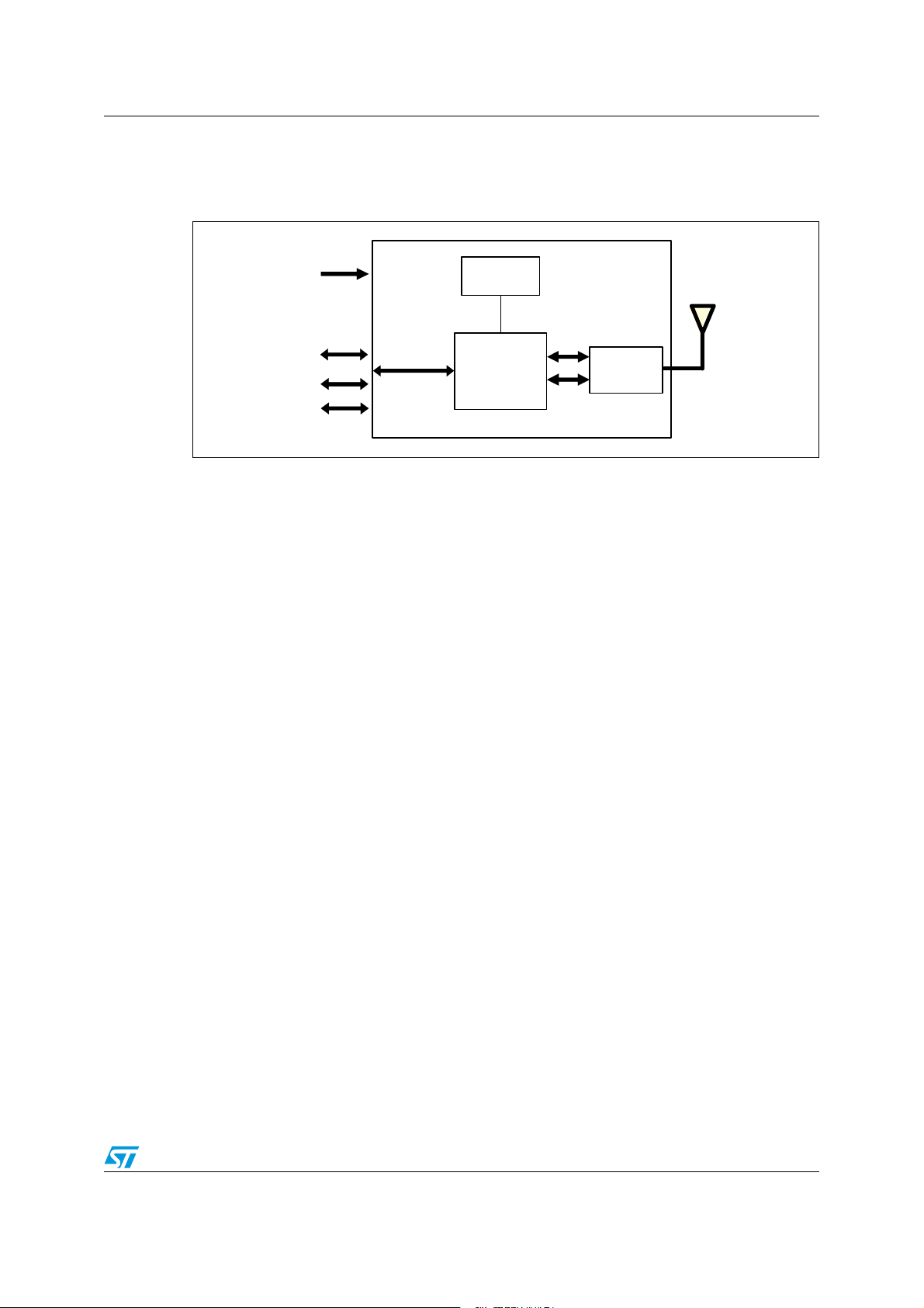
SPZB260C-PRO Block diagram
1 Block diagram
Figure 1. SPZB260C-PRO block diagram
6
$$
3)&
30)<5!24
#/.423)'.
-(Z
84!,
%-
4RANSCEIVER
2&
ANTENNA
"ALUN
&ILTER
!-V
Doc ID 17301 Rev 1 3/15

Pin information SPZB260C-PRO
2 Pin information
2.1 Pin connections
Figure 2. Pin connection diagram
4/15 Doc ID 17301 Rev 1
SPZB260C-PRO Pin information
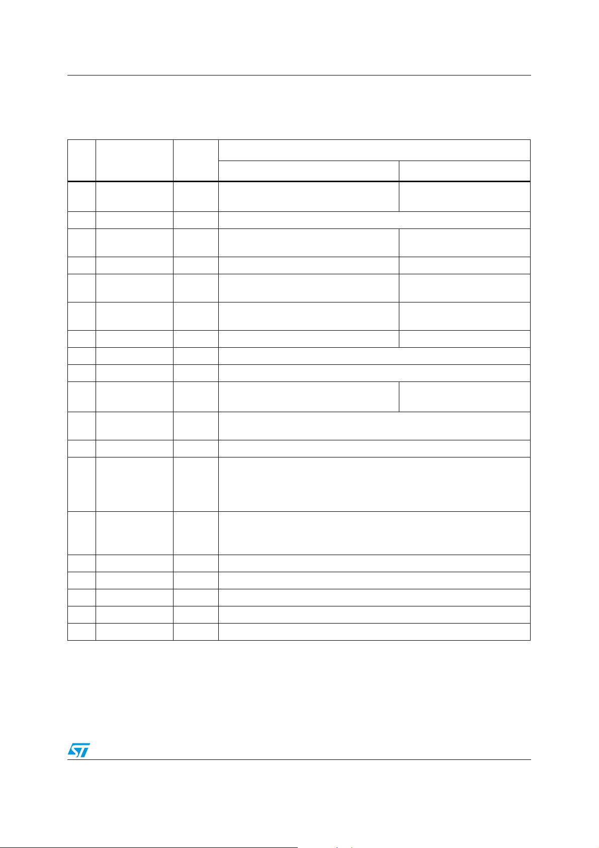
2.2 Pin description
Table 1. Pin description
Description
Pin n Pin name Direction
SPI mode UART mode
1 RTS O Not used
RTS signal
(10 kΩ pull-up to VDD)
2 RSTB I Active low reset (a pull-up of 10 kΩ typ is provided with 10 nF to GND)
3 HOST_INT / RXD O /I
Host interrupt signal (from ZB module to
host) - SPI mode
RXD signal
4 SPI_SSEL / CTS I SPI slave select (from host to ZB module) CTS signal
5 SPI MOSI I
6 SPI MISO O
SPI data, master out/slave in (from host to
ZB module)
SPI data, master in/slave out (from ZB
module to host)
Not used
Not used
7 SPI_CLK I SPI clock Not used
8 GND --- Ground
9
10 TXD O Not used
11 SIF_CLK I
VDD --- Input power supply
TXD signal
(10 kΩ pull-up to VDD)
Non-intrusive debug interface. Serial interface clock signal (internal pulldown)
12 SIF_MISO O Non-intrusive debug interface. Serial interface master in/slave out
Non-intrusive debug interface
13 SIF_MOSI I
Serial interface master out/slave in
To guarantee proper signal level when in deep sleep mode, a 10 kΩ resistor
to GND is included
Non-intrusive debug Interface
14 SIF_LOADB I/O
Serial interface load strobe (open collector with internal pull-up).
To improve noise immunity, a 10 kΩ resistor to Vdd is included
15 PTI_EN O Frame signal of packet trace interface (PTI)
16 PTI_DATA O Data signal of packet trace interface (PTI)
17 WAKE I Wake interrupt signal from host to ZB module
18 ACTIVITY O Activity signal for application debug /monitor
19 SDBG O Spare debug signal
Doc ID 17301 Rev 1 5/15
 Loading...