

Low data rate, low power sub-1GHZ transceiver
QFN20
Features
■ Frequency bands: 150-174 MHz, 300-348
MHz, 387-470 MHz, 779-956 MHz
■ Modulation schemes: 2-FSK, GFSK, MSK,
GMSK, OOK, and ASK
■ Air data rate from 1 to 500 kbps
■ Very low power consumption (9 mA RX and 21
mA TX at +11 dBm)
■ Programmable RX digital filter from 6 kHz to
800 kHz
■ Programmable channel spacing (12.5 kHz
min.)
■ Excellent performance of receiver sensitivity (-
120 dBm), selectivity, and blocking
■ Programmable output power up to +11 dBm
■ Fast startup and frequency synthesizer settling
time (6 µs)
■ Frequency offset compensation
■ Integrated temperature sensor
■ Battery indicator and low battery detector
■ RX and TX FIFO buffer (96 bytes each)
■ Configurability via SPI interface
■ Automatic acknowledgement, retransmission,
and timeout protocol engine
■ AES 128-bit encryption co-processor
■ Antenna diversity algorithm
■ Fully integrated ultra low power RC oscillator
■ Wake-up on internal timer and wake-up on
external event
■ Flexible packet length with dynamic payload
length
■ Sync word detection
■ Address check
■ Automatic CRC handling
■ FEC with interleaving
SPIRIT1
Datasheet — preliminary data
■ Digital RSSI output
■ Programmable carrier sense (CS) indicator
■ Automatic clear channel assessment (CCA)
before transmitting (for listen-before-talk
systems). Embedded CSMA/CA protocol
■ Programmable preamble quality indicator
(PQI)
■ Link quality indication (LQI)
■ Whitening and de-whitening of data
■ Wireless M-BUS, EN 300 220, FCC CFR47 15
(15.205, 15.209, 15.231, 15.247, 15.249), and
ARIB STD T-67, T93, T-108 compliant
■ QFN20 4x4 mm RoHS package
■ Operating temperature range from -40 °C to 85
°C
Applications
■ AMR (automatic meter reading)
■ Home and building automation
■ WSN (wireless sensors network)
■ Industrial monitoring and control
■ Wireless fire and security alarm systems
■ Point-to-point wireless link
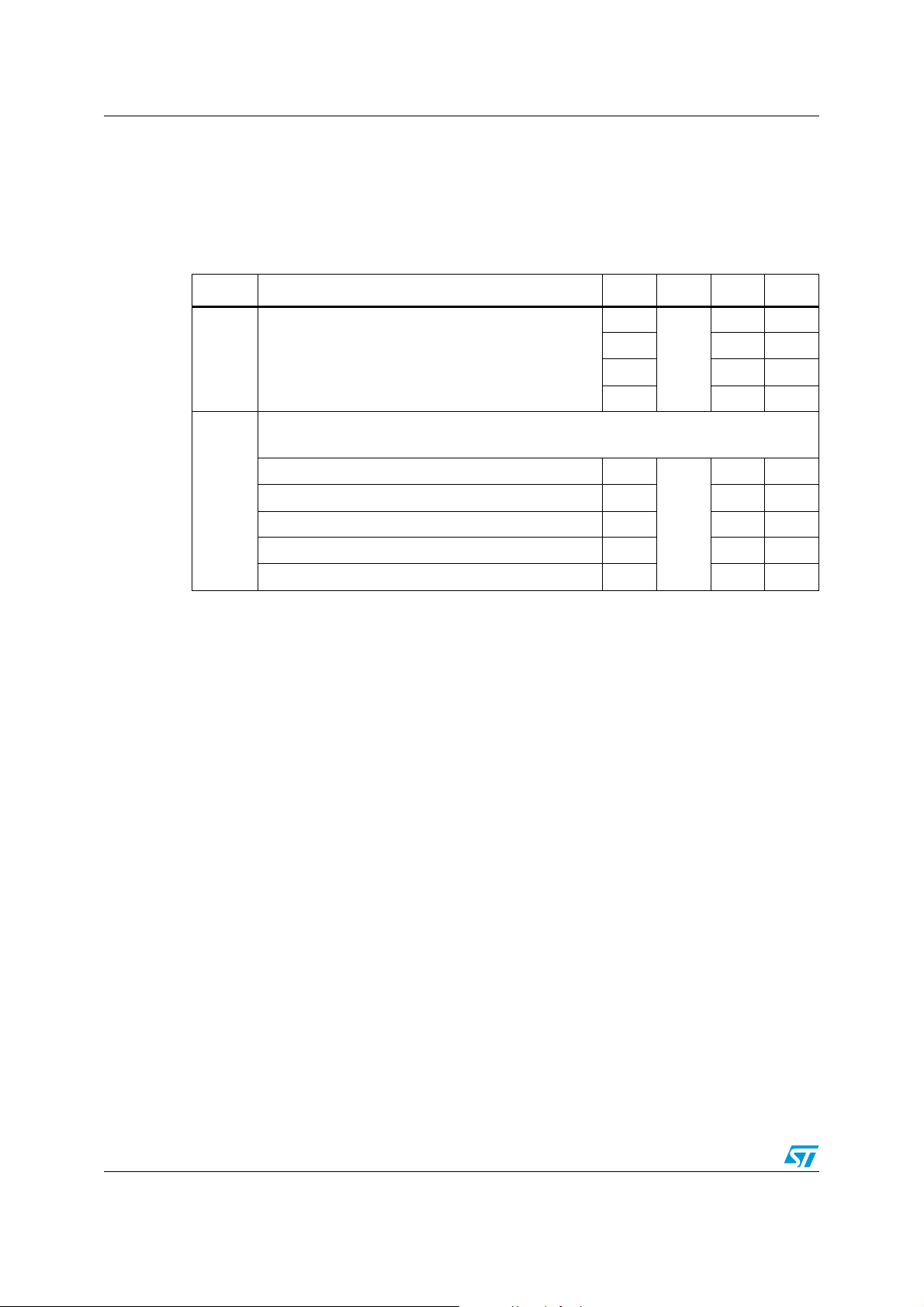
Table 1. Device summary
Order code Package Packing
SPIRIT1QTR QFN20 Tape and reel
April 2012 Doc ID 022758 Rev 2 1/91
This is preliminary information on a new product now in development or undergoing evaluation. Details are subject to
change without notice.
www.st.com
91

Contents SPIRIT1
Contents
1 Description . . . . . . . . . . . . . . . . . . . . . . . . . . . . . . . . . . . . . . . . . . . . . . . . . 5
2 Introduction . . . . . . . . . . . . . . . . . . . . . . . . . . . . . . . . . . . . . . . . . . . . . . . . 6
3 Typical application diagram and pin description . . . . . . . . . . . . . . . . . . 8
3.1 Typical application diagram . . . . . . . . . . . . . . . . . . . . . . . . . . . . . . . . . . . . 8
4 Pinout . . . . . . . . . . . . . . . . . . . . . . . . . . . . . . . . . . . . . . . . . . . . . . . . . . . . 10
5 Absolute maximum ratings and thermal data . . . . . . . . . . . . . . . . . . . 11
6 Characteristics . . . . . . . . . . . . . . . . . . . . . . . . . . . . . . . . . . . . . . . . . . . . 12
6.1 General characteristics . . . . . . . . . . . . . . . . . . . . . . . . . . . . . . . . . . . . . . . 12
6.2 Electrical specifications . . . . . . . . . . . . . . . . . . . . . . . . . . . . . . . . . . . . . . 12
6.2.1 Electrical characteristics . . . . . . . . . . . . . . . . . . . . . . . . . . . . . . . . . . . . 12
6.2.2 Digital SPI . . . . . . . . . . . . . . . . . . . . . . . . . . . . . . . . . . . . . . . . . . . . . . . 13
6.2.3 RF receiver . . . . . . . . . . . . . . . . . . . . . . . . . . . . . . . . . . . . . . . . . . . . . . 14
6.2.4 RF transmitter . . . . . . . . . . . . . . . . . . . . . . . . . . . . . . . . . . . . . . . . . . . . 17
6.2.5 Crystal oscillator . . . . . . . . . . . . . . . . . . . . . . . . . . . . . . . . . . . . . . . . . . 21
6.2.6 Sensors . . . . . . . . . . . . . . . . . . . . . . . . . . . . . . . . . . . . . . . . . . . . . . . . . 22
7 Operating modes . . . . . . . . . . . . . . . . . . . . . . . . . . . . . . . . . . . . . . . . . . . 24
7.1 Reset sequence . . . . . . . . . . . . . . . . . . . . . . . . . . . . . . . . . . . . . . . . . . . . 27
7.2 Timer usage . . . . . . . . . . . . . . . . . . . . . . . . . . . . . . . . . . . . . . . . . . . . . . . 28
7.3 Low duty cycle reception mode . . . . . . . . . . . . . . . . . . . . . . . . . . . . . . . . 28
7.4 CSMA/CA engine . . . . . . . . . . . . . . . . . . . . . . . . . . . . . . . . . . . . . . . . . . . 29
8 Block description . . . . . . . . . . . . . . . . . . . . . . . . . . . . . . . . . . . . . . . . . . 33
8.1 Power management . . . . . . . . . . . . . . . . . . . . . . . . . . . . . . . . . . . . . . . . . 33
8.2 Power-on-reset (POR) . . . . . . . . . . . . . . . . . . . . . . . . . . . . . . . . . . . . . . . 33
8.3 Low battery indicator . . . . . . . . . . . . . . . . . . . . . . . . . . . . . . . . . . . . . . . . 33
8.4 Voltage reference . . . . . . . . . . . . . . . . . . . . . . . . . . . . . . . . . . . . . . . . . . . 33
8.5 Oscillator and RF synthesizer . . . . . . . . . . . . . . . . . . . . . . . . . . . . . . . . . 33
8.6 RCO: features and calibration . . . . . . . . . . . . . . . . . . . . . . . . . . . . . . . . . 36
2/91 Doc ID 022758 Rev 2

SPIRIT1 Contents
8.6.1 RC oscillator calibration . . . . . . . . . . . . . . . . . . . . . . . . . . . . . . . . . . . . . 36
8.7 AFC . . . . . . . . . . . . . . . . . . . . . . . . . . . . . . . . . . . . . . . . . . . . . . . . . . . . . 37
8.8 Receiver . . . . . . . . . . . . . . . . . . . . . . . . . . . . . . . . . . . . . . . . . . . . . . . . . . 37
8.9 Transmitter . . . . . . . . . . . . . . . . . . . . . . . . . . . . . . . . . . . . . . . . . . . . . . . . 37
8.10 Temperature sensors (TS) . . . . . . . . . . . . . . . . . . . . . . . . . . . . . . . . . . . . 38
8.11 AES encryption co-processor . . . . . . . . . . . . . . . . . . . . . . . . . . . . . . . . . . 38
9 Transmission and reception . . . . . . . . . . . . . . . . . . . . . . . . . . . . . . . . . . 40
9.1 PA configuration . . . . . . . . . . . . . . . . . . . . . . . . . . . . . . . . . . . . . . . . . . . . 40
9.2 RF channel frequency settings . . . . . . . . . . . . . . . . . . . . . . . . . . . . . . . . . 41
9.3 RX timeout management . . . . . . . . . . . . . . . . . . . . . . . . . . . . . . . . . . . . . 43
9.4 Intermediate frequency setting . . . . . . . . . . . . . . . . . . . . . . . . . . . . . . . . . 44
9.5 Modulation scheme . . . . . . . . . . . . . . . . . . . . . . . . . . . . . . . . . . . . . . . . . 45
9.5.1 Data rate . . . . . . . . . . . . . . . . . . . . . . . . . . . . . . . . . . . . . . . . . . . . . . . . 47
9.5.2 RX channel bandwidth . . . . . . . . . . . . . . . . . . . . . . . . . . . . . . . . . . . . . . 47
9.6 Data coding and integrity check process . . . . . . . . . . . . . . . . . . . . . . . . . 48
9.6.1 FEC . . . . . . . . . . . . . . . . . . . . . . . . . . . . . . . . . . . . . . . . . . . . . . . . . . . . 48
9.6.2 CRC . . . . . . . . . . . . . . . . . . . . . . . . . . . . . . . . . . . . . . . . . . . . . . . . . . . . 48
9.6.3 Data whitening . . . . . . . . . . . . . . . . . . . . . . . . . . . . . . . . . . . . . . . . . . . . 49
9.6.4 Data padding . . . . . . . . . . . . . . . . . . . . . . . . . . . . . . . . . . . . . . . . . . . . . 49
9.7 Packet handler engine . . . . . . . . . . . . . . . . . . . . . . . . . . . . . . . . . . . . . . . 50
9.7.1 STack packet . . . . . . . . . . . . . . . . . . . . . . . . . . . . . . . . . . . . . . . . . . . . . 50
9.7.2 Wireless M-Bus packet (W M-BUS, EN13757-4) . . . . . . . . . . . . . . . . . . 51
9.7.3 Basic packet . . . . . . . . . . . . . . . . . . . . . . . . . . . . . . . . . . . . . . . . . . . . . . 52
9.7.4 Automatic packet filtering . . . . . . . . . . . . . . . . . . . . . . . . . . . . . . . . . . . . 53
9.7.5 Link layer protocol . . . . . . . . . . . . . . . . . . . . . . . . . . . . . . . . . . . . . . . . . 54
9.8 Data modes . . . . . . . . . . . . . . . . . . . . . . . . . . . . . . . . . . . . . . . . . . . . . . . 55
9.9 Data FIFO . . . . . . . . . . . . . . . . . . . . . . . . . . . . . . . . . . . . . . . . . . . . . . . . . 56
9.10 Receiver quality indicators . . . . . . . . . . . . . . . . . . . . . . . . . . . . . . . . . . . . 58
9.10.1 RSSI . . . . . . . . . . . . . . . . . . . . . . . . . . . . . . . . . . . . . . . . . . . . . . . . . . . 58
9.10.2 Carrier sense . . . . . . . . . . . . . . . . . . . . . . . . . . . . . . . . . . . . . . . . . . . . . 58
9.10.3 LQI . . . . . . . . . . . . . . . . . . . . . . . . . . . . . . . . . . . . . . . . . . . . . . . . . . . . . 59
9.10.4 PQI . . . . . . . . . . . . . . . . . . . . . . . . . . . . . . . . . . . . . . . . . . . . . . . . . . . . . 59
9.10.5 SQI . . . . . . . . . . . . . . . . . . . . . . . . . . . . . . . . . . . . . . . . . . . . . . . . . . . . . 59
9.11 Antenna diversity . . . . . . . . . . . . . . . . . . . . . . . . . . . . . . . . . . . . . . . . . . . 60
Doc ID 022758 Rev 2 3/91

Contents SPIRIT1
9.12 Frequency hopping . . . . . . . . . . . . . . . . . . . . . . . . . . . . . . . . . . . . . . . . . . 61
10 MCU interface . . . . . . . . . . . . . . . . . . . . . . . . . . . . . . . . . . . . . . . . . . . . . 62
10.1 Serial peripheral interface . . . . . . . . . . . . . . . . . . . . . . . . . . . . . . . . . . . . 62
10.2 Interrupts . . . . . . . . . . . . . . . . . . . . . . . . . . . . . . . . . . . . . . . . . . . . . . . . . 64
10.3 GPIOs . . . . . . . . . . . . . . . . . . . . . . . . . . . . . . . . . . . . . . . . . . . . . . . . . . . 65
10.4 MCU clock . . . . . . . . . . . . . . . . . . . . . . . . . . . . . . . . . . . . . . . . . . . . . . . . 67
11 Register table . . . . . . . . . . . . . . . . . . . . . . . . . . . . . . . . . . . . . . . . . . . . . . 69
12 Package mechanical data . . . . . . . . . . . . . . . . . . . . . . . . . . . . . . . . . . . . 86
13 Revision history . . . . . . . . . . . . . . . . . . . . . . . . . . . . . . . . . . . . . . . . . . . 88
4/91 Doc ID 022758 Rev 2

SPIRIT1 List of tables
List of tables
Table 1. Device summary . . . . . . . . . . . . . . . . . . . . . . . . . . . . . . . . . . . . . . . . . . . . . . . . . . . . . . . . . . 1
Table 2. Description of the external components of the typical application diagram . . . . . . . . . . . . . 8
Table 3. Pinout description . . . . . . . . . . . . . . . . . . . . . . . . . . . . . . . . . . . . . . . . . . . . . . . . . . . . . . . . 10
Table 4. Absolute maximum ratings . . . . . . . . . . . . . . . . . . . . . . . . . . . . . . . . . . . . . . . . . . . . . . . . . 11
Table 5. Thermal data. . . . . . . . . . . . . . . . . . . . . . . . . . . . . . . . . . . . . . . . . . . . . . . . . . . . . . . . . . . . 11
Table 6. Recommended operating conditions . . . . . . . . . . . . . . . . . . . . . . . . . . . . . . . . . . . . . . . . . 11
Table 7. General characteristics . . . . . . . . . . . . . . . . . . . . . . . . . . . . . . . . . . . . . . . . . . . . . . . . . . . . 12
Table 8. Power consumption . . . . . . . . . . . . . . . . . . . . . . . . . . . . . . . . . . . . . . . . . . . . . . . . . . . . . . 13
Table 9. Digital SPI input and output (SDO, SDI, SCLK, CSn, and SDN) and GPIO specification
(GPIO_1-4) . . . . . . . . . . . . . . . . . . . . . . . . . . . . . . . . . . . . . . . . . . . . . . . . . . . . . . . . . . . . . 13
Table 10. RF receiver characteristics . . . . . . . . . . . . . . . . . . . . . . . . . . . . . . . . . . . . . . . . . . . . . . . . . 14
Table 11. RF transmitter characteristics . . . . . . . . . . . . . . . . . . . . . . . . . . . . . . . . . . . . . . . . . . . . . . . 17
Table 12. Crystal oscillator characteristics . . . . . . . . . . . . . . . . . . . . . . . . . . . . . . . . . . . . . . . . . . . . . 21
Table 13. Ultra low power RC oscillator . . . . . . . . . . . . . . . . . . . . . . . . . . . . . . . . . . . . . . . . . . . . . . . 22
Table 14. N-Fractional ÓÄ frequency synthesizer characteristics . . . . . . . . . . . . . . . . . . . . . . . . . . . 22
Table 15. Analog temperature sensor characteristics . . . . . . . . . . . . . . . . . . . . . . . . . . . . . . . . . . . . 22
Table 16. Battery indicator and low battery detector . . . . . . . . . . . . . . . . . . . . . . . . . . . . . . . . . . . . . 23
Table 17. States . . . . . . . . . . . . . . . . . . . . . . . . . . . . . . . . . . . . . . . . . . . . . . . . . . . . . . . . . . . . . . . . . 25
Table 18. Commands list . . . . . . . . . . . . . . . . . . . . . . . . . . . . . . . . . . . . . . . . . . . . . . . . . . . . . . . . . . 26
Table 19. POR parameters . . . . . . . . . . . . . . . . . . . . . . . . . . . . . . . . . . . . . . . . . . . . . . . . . . . . . . . . . 28
Table 20. SPIRIT1 timers description and duration . . . . . . . . . . . . . . . . . . . . . . . . . . . . . . . . . . . . . . 28
Table 21. Programmability of trans-conductance at startup . . . . . . . . . . . . . . . . . . . . . . . . . . . . . . . . 34
Table 22. CP word look-up . . . . . . . . . . . . . . . . . . . . . . . . . . . . . . . . . . . . . . . . . . . . . . . . . . . . . . . . . 35
Table 23. PA_level . . . . . . . . . . . . . . . . . . . . . . . . . . . . . . . . . . . . . . . . . . . . . . . . . . . . . . . . . . . . . . . 40
Table 24. Frequency threshold . . . . . . . . . . . . . . . . . . . . . . . . . . . . . . . . . . . . . . . . . . . . . . . . . . . . . . 43
Table 25. RX timeout stop condition configuration . . . . . . . . . . . . . . . . . . . . . . . . . . . . . . . . . . . . . . . 43
Table 26. IF_OFFSET settings . . . . . . . . . . . . . . . . . . . . . . . . . . . . . . . . . . . . . . . . . . . . . . . . . . . . . . 45
Table 27. CHFLT_M and CHFLT_E value for channel filter bandwidth (in kHz, for fclk = 26 MHz) . . 47
Table 28. Packet configuration . . . . . . . . . . . . . . . . . . . . . . . . . . . . . . . . . . . . . . . . . . . . . . . . . . . . . . 54
Table 29. MCU clock vs. state . . . . . . . . . . . . . . . . . . . . . . . . . . . . . . . . . . . . . . . . . . . . . . . . . . . . . . 64
Table 30. Interrupts. . . . . . . . . . . . . . . . . . . . . . . . . . . . . . . . . . . . . . . . . . . . . . . . . . . . . . . . . . . . . . . 64
Table 31. Digital outputs . . . . . . . . . . . . . . . . . . . . . . . . . . . . . . . . . . . . . . . . . . . . . . . . . . . . . . . . . . . 65
Table 32. Digital inputs . . . . . . . . . . . . . . . . . . . . . . . . . . . . . . . . . . . . . . . . . . . . . . . . . . . . . . . . . . . . 67
Table 33. MCU_CK_CONF configuration register . . . . . . . . . . . . . . . . . . . . . . . . . . . . . . . . . . . . . . . 67
Table 34. MCU clock vs. state . . . . . . . . . . . . . . . . . . . . . . . . . . . . . . . . . . . . . . . . . . . . . . . . . . . . . . 68
Table 35. General configuration registers. . . . . . . . . . . . . . . . . . . . . . . . . . . . . . . . . . . . . . . . . . . . . . 69
Table 36. Radio configuration registers (analog blocks). . . . . . . . . . . . . . . . . . . . . . . . . . . . . . . . . . . 71
Table 37. Radio configuration registers (digital blocks) . . . . . . . . . . . . . . . . . . . . . . . . . . . . . . . . . . . 73
Table 38. Packet/protocol configuration registers. . . . . . . . . . . . . . . . . . . . . . . . . . . . . . . . . . . . . . . . 75
Table 39. Frequently used registers . . . . . . . . . . . . . . . . . . . . . . . . . . . . . . . . . . . . . . . . . . . . . . . . . . 82
Table 40. General information . . . . . . . . . . . . . . . . . . . . . . . . . . . . . . . . . . . . . . . . . . . . . . . . . . . . . . 85
Table 41. QFN20 (4 x 4 mm.) mechanical data . . . . . . . . . . . . . . . . . . . . . . . . . . . . . . . . . . . . . . . . . 86
Table 42. Document revision history . . . . . . . . . . . . . . . . . . . . . . . . . . . . . . . . . . . . . . . . . . . . . . . . . 88
Doc ID 022758 Rev 2 5/91

List of figures SPIRIT1
List of figures
Figure 1. SPIRIT1 block diagram . . . . . . . . . . . . . . . . . . . . . . . . . . . . . . . . . . . . . . . . . . . . . . . . . . . . . 6
Figure 2. Suggested application diagram . . . . . . . . . . . . . . . . . . . . . . . . . . . . . . . . . . . . . . . . . . . . . . 8
Figure 3. Diagram and transition . . . . . . . . . . . . . . . . . . . . . . . . . . . . . . . . . . . . . . . . . . . . . . . . . . . . 24
Figure 4. Power-on reset timing and limits. . . . . . . . . . . . . . . . . . . . . . . . . . . . . . . . . . . . . . . . . . . . . 27
Figure 5. LDCR mode timing . . . . . . . . . . . . . . . . . . . . . . . . . . . . . . . . . . . . . . . . . . . . . . . . . . . . . . . 29
Figure 6. CSMA flowchart . . . . . . . . . . . . . . . . . . . . . . . . . . . . . . . . . . . . . . . . . . . . . . . . . . . . . . . . . 31
Figure 7. Shaping of ASK signal . . . . . . . . . . . . . . . . . . . . . . . . . . . . . . . . . . . . . . . . . . . . . . . . . . . . 38
Figure 8. Output power ramping configuration. . . . . . . . . . . . . . . . . . . . . . . . . . . . . . . . . . . . . . . . . . 41
Figure 9. LFSR block diagram . . . . . . . . . . . . . . . . . . . . . . . . . . . . . . . . . . . . . . . . . . . . . . . . . . . . . 49
Figure 10. Threshold of the linear FIFO. . . . . . . . . . . . . . . . . . . . . . . . . . . . . . . . . . . . . . . . . . . . . . . . 57
Figure 11. SPI “write” operation . . . . . . . . . . . . . . . . . . . . . . . . . . . . . . . . . . . . . . . . . . . . . . . . . . . . . . 62
Figure 12. SPI “read” operation . . . . . . . . . . . . . . . . . . . . . . . . . . . . . . . . . . . . . . . . . . . . . . . . . . . . . . 63
Figure 13. SPI “command” operation. . . . . . . . . . . . . . . . . . . . . . . . . . . . . . . . . . . . . . . . . . . . . . . . . . 63
Figure 14. QFN20 (4 x 4 mm.) dimension . . . . . . . . . . . . . . . . . . . . . . . . . . . . . . . . . . . . . . . . . . . . . . 87
6/91 Doc ID 022758 Rev 2

SPIRIT1 Description
1 Description
The SPIRIT1 is a very low-power RF transceiver, intended for RF wireless applications in
the sub-1 GHz band. It is designed to operate both in the license-free ISM and SRD
frequency bands at 169, 315, 433, 868, and 915 MHz, but can also be programmed to
operate at other additional frequencies in the 300-348 MHz, 387-470 MHz, and 779-956
MHz bands. The air data rate is programmable from 1 to 500 kbps, and the SPIRIT1 can be
used in systems with channel spacing of 12.5/25 kHz, complying with the EN 300 220
standard. It uses a very small number of discrete external components and integrates a
configurable baseband modem, which supports data management, modulation, and
demodulation. The data management handles the data in the proprietary fully
programmable packet format also allows the M-Bus standard compliance format (all
performance classes).
However, the SPIRIT1 can perform cyclic redundancy checks on the data as well as FEC
encoding/decoding on the packets. The SPIRIT1 provides an optional automatic
acknowledgement, retransmission, and timeout protocol engine in order to reduce overall
system costs by handling all the high-speed link layer operations.
Moreover, the SPIRIT1 supports an embedded CSMA/CA engine. An AES 128-bit
encryption co-processor is available for secure data transfer. The SPIRIT1 fully supports
antenna diversity with an integrated antenna switching control algorithm. The SPIRIT1
supports different modulation schemes: 2-FSK, GFSK, OOK, ASK, and MSK.
Transmitted/received data bytes are buffered in two different three-level FIFOs (TX FIFO
and RX FIFO), accessible via the SPI interface for host processing.
Doc ID 022758 Rev 2 7/91
Introduction SPIRIT1
>E
DKh>dKZ
W
&ZY
^zEd,
Ϭ
ϵϬ
DKh>dKZ
Zy&/&KƐdy&/&KƐ
^W/
Z'/^dZ^DW
'W/K
/EdZ&
Z/KKEdZK>
ZK
d>/E<>zZ
ŝŐŝƚĂů>K
sK>K
W>>>K
WZK'>K
>K
>ŽǁWŽǁĞƌ
ŝŐŝƚĂů>K
dDW^E^
dy
ZyŶ
ZyƉ
D/^K
DK^/
^><
^Ŷ
'W/Kͺϯ
'W/KͺϮ
'W/Kͺϭ
'W/KͺϬ
sZ'
sd
^DW^džƚϭ
^DW^džƚϮ
y/E
yKhd
^E
s
d
Z/^
WKZ
^
>K
ϭsϱ
EdZ>
/^
KZ
;ƌĂǁͿ
KZ
;ĂĐĐͿ
>
/'/d>>K<
yK ZD
Khdŝǀ> K
^DW^
/'
/K
!-6
2 Introduction
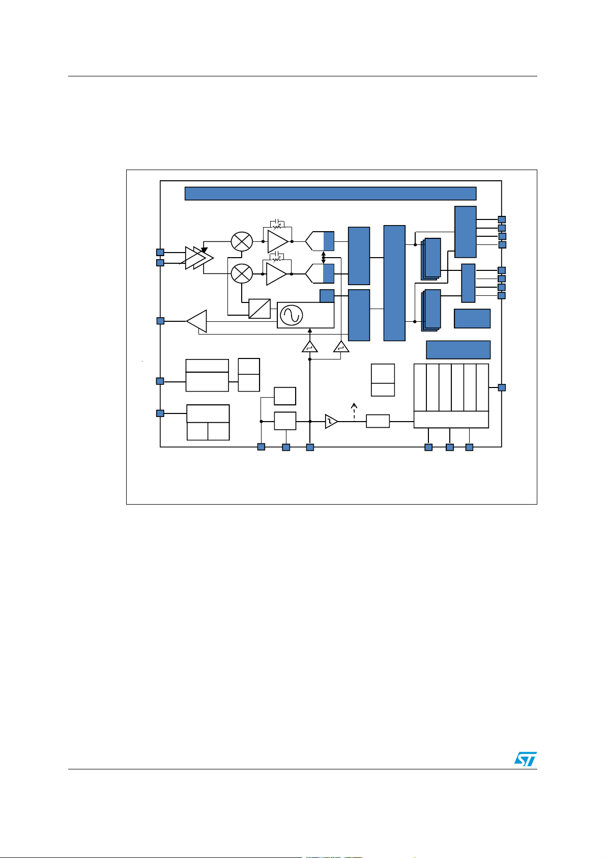
A simplified block diagram of the SPIRIT1 is shown in Figure 1.
Figure 1. SPIRIT1 block diagram
The receiver architecture is direct conversion. The received RF signal is amplified by a two-
stage low-noise amplifier (LNA) and down-converted in quadrature (I and Q) to the
intermediate frequency (IF). LNA and IF amplifiers make up the RX front-end (RXFE) and
have programmable gain. At IF, I/Q signals are digitized by ADCs. The demodulated data is
then provided to an external MCU either through the 96-byte RX FIFO, readable via SPI, or
directly using a programmable GPIO pin. A 128-bit AES co-processor is available to perform
(offline) data encryption/decryption to secure data transfer.
The transmitter part of the SPIRIT1 is based on direct synthesis of the RF frequency. The
power amplifier (PA) input is the LO generated by the RF synthesizer, while the output level
can be configured between -30 dBm and +11 dBm in 0.5 dB steps. The data to be
transmitted can be provided by an external MCU either through the 96-byte TX FIFO
writable via SPI, or directly using a programmable GPIO pin. The SPIRIT1 supports
frequency hopping, TX/RX and antenna diversity switch control, extending the link range
and improving performance.
The SPIRIT1 has a very efficient power management (PM) system.
8/91 Doc ID 022758 Rev 2

SPIRIT1 Introduction
An integrated switched mode power supply (SMPS) regulator allows operation from a
battery voltage ranging from +1.8 V to +3.6 V, and with power conversion efficiency of at
least 80%.
A crystal must be connected between XIN and XOUT. It is digitally configurable to operate
with different crystals. As an alternative, an external clock signal can be used to feed XIN for
proper operation. The SPIRIT1 also has an integrated low-power RC oscillator, generating
the 34.7 kHz signal used as a clock for the slowest timeouts (i.e. sleeping and backoff).
A standard 4-pin SPI bus is used to communicate with the external MCU. Four configurable
general purpose I/Os are available.
Doc ID 022758 Rev 2 9/91
Typical application diagram and pin description SPIRIT1
1.8V÷3.6V power supply
C0
C13
1 GPIO_0 SDN 15
SMPS Ext1 14
SMPS Ext2 13
TX 12
GND_PA 11
2 MISO
3 MOSI
4 SCLK
5 CSn
GPIO_1 20
GPIO_2 19
GPIO_3 18
VREG 17
VBAT 16
8 VBAT
6 XOUT
7 XIN
9 RFp
10 RFn
DIGITAL INTERFACE
SPIRIT1
DIE ATTACH PAD:
C9
C6
XTAL
C11
L7
Antenna
(50Ω )
L0
L1
L2
L3
C1
C2
C3
C5
L4
C4
L5
C10
L6
C7 C8
C0
L8
C12
C13
C15
C14
L9
AM09258V1
3 Typical application diagram and pin description
3.1 Typical application diagram
Figure 2. Suggested application diagram
Table 2. Description of the external components of the typical application
diagram
Components Description
C0 Decoupling capacitor for on-chip voltage regulator to digital part
C1, C2, C3, C14, C15 RF LC filter/matching capacitors
C4, C5 RF balun/matching capacitors
C6, C7, C8 RF balun/matching DC blocking capacitors
C9, C10 Crystal loading capacitors
C11, C12, C13 SMPS LC filter capacitor
L0 RF choke inductor
L1, L2, L3, L9 RF LC filter/matching inductors
L4, L5, L6 RF balun/matching inductors
10/91 Doc ID 022758 Rev 2

SPIRIT1 Typical application diagram and pin description
Table 2. Description of the external components of the typical application diagram
(continued)
Components Description
L7, L8 SMPS LC filter inductor
XTAL 24, 26, 48, 52 MHz
Ta bl e 2 assumes to cover all the frequency bands using only four sets of external
components.
Doc ID 022758 Rev 2 11/91

Pinout SPIRIT1
4 Pinout
Table 3. Pinout description
Pin Name I/O Description
1 GPIO_0 I/O See description of GPIOs below
2 MISO O SPI data output pin
3 MOSI I SPI data input pin
4 SCLK I SPI clock input pin
5 CSn I SPI chip select
6XOUTO
7XINI
8 VBAT VDD +1.8 V to +3.6 V input supply voltage
9RXpI
10 RXn I
11 GND_PA GND Ground for PA
12 TX O RF output signal
13 SMPS Ext2 I Regulated DC-DC voltage input
14 SMPS Ext1 O DC-DC output pin
15 SDN I
16 VBAT VDD +1.8 V to +3.6 V input supply voltage
17 VREG
18 GPIO3 I/O General purpose I/O that may be configured through the SPI
19 GPIO2 I/O
20 GPIO1 I/O
21 GND GND Exposed pad ground pin
(1)
VDD Regulated output voltage. A 100 nF decoupling capacitor is required
Crystal oscillator output. Connect to an external 26 MHz crystal or
leave floating if driving the XIN pin with an external signal source
Crystal oscillator input. Connect to an external 26 MHz crystal or to
an external source. If using an external clock source with no crystal,
DC coupling with a nominal 0.2 VDC level is recommended with
minimum AC amplitude of 400 mVpp
Differential RF input signal for the LNA. See application diagram for a
typical matching network
Shutdown input pin. 0-VDD V digital input. SDN should be = ‘0’ in all
modes except shutdown mode. When SDN =’1’ the SPIRIT1 is
completely shut down and the contents of the registers are lost
registers to perform various functions, including:
– MCU clock output
– FIFO status flags
– Wake-up input
– Battery level detector
– TX-RX external switch control
– Antenna diversity control
– Temperature sensor output
1. This pin is intended for use with the SPIRIT1 only. It cannot be used to provide supply voltage to other devices.
12/91 Doc ID 022758 Rev 2
SPIRIT1 Absolute maximum ratings and thermal data
5 Absolute maximum ratings and thermal data
Absolute maximum ratings are those values above which damage to the device may occur.
Functional operation under these conditions is not implied. All voltages are referred to GND.
Table 4. Absolute maximum ratings
Pin Parameter Value Unit
8,14,16 Supply voltage and SMPS output -0.3 to +3.6 V
17 DC voltage on VREG -0.3 to +1.4 V
1,3,4,5,15,18,19,20 DC voltage on digital input pins -0.3 to +3.6 V
2 DC voltage on digital output pins -0.3 to +3.6 V
11 DC voltage on analog pins -0.3 to +3.6 V
6,7,9,10 DC voltage on RX/XTAL pins -0.3 to +1.4 V
13 DC voltage on SMPS Ext2 pin -0.3 to +1.4 V
12 DC voltage on TX pin -0.3 to +3.6 V
T
STG
V
ESD-HBM
Storage temperature range -40 to +125 °C
Electrostatic discharge voltage ±1.0 KV
Table 5. Thermal data
Symbol Parameter QFN20 Unit
R
thj-amb
Thermal resistance junction-ambient 45 °C/W
Table 6. Recommended operating conditions
Symbol Parameter Min. Typ. Max. Unit
V
BAT
T
Operating battery supply voltage 1.8 3 3.6 V
Operating ambient temperature range -40 85 °C
A
Doc ID 022758 Rev 2 13/91
Characteristics SPIRIT1
6 Characteristics
6.1 General characteristics
Table 7. General characteristics
Symbol Parameter Min. Typ. Max. Unit
FREQ Frequency range
Air data rate for each modulation scheme
Optional Manchester and 3 out of 6 encoding/decoding can be selected
2-FSK 1
DR
GMSK (BT=1, BT=0.5) 1 500 kBaud
GFSK (BT=1, BT=0.5) 1 500 kBaud
MSK 1 500 kBaud
OOK/ASK 1 250 kBaud
6.2 Electrical specifications
6.2.1 Electrical characteristics
Characteristics measured over recommended operating conditions unless otherwise
specified. Typical values are referred to T
to a 50 Ohm antenna connector, via the reference design.
= 25 °C, V
A
150
300 348 MHz
387 470 MHz
779 956 MHz
= 3.0 V. All performance is referred
BAT
174 MHz
-
500 kBaud
-
14/91 Doc ID 022758 Rev 2

SPIRIT1 Characteristics
Table 8. Power consumption
Symbol Parameter Test conditions Min. Typ. Max. Unit
RX
(1)
(1)
(1)
(1)
(1)
(1)
2.5
650 nA
950 nA
400 µA
4.5 mA
9mA
21
22
19.5
21
6
6.5
7
7
nA
-
mA
I
BAT
1. See Table 17.
Supply current
Shutdown
Standby
Sleep
Ready (default mode)
Tu ni n g
(1)
TX
+11 dBm 169 MHz
(1)
TX
+11 dBm 315 MHz
(1)
TX
+11 dBm 433 MHz
(1)
TX
+11 dBm 868 MHz
(1)
TX
-8 dBm 169 MHz
(1)
TX
-8 dBm 315 MHz
(1)
TX
-7 dBm 433 MHz
(1)
TX
-7 dBm 868 MHz
6.2.2 Digital SPI
Table 9. Digital SPI input and output (SDO, SDI, SCLK, CSn, and SDN) and GPIO
Symbol Parameter Test condition Min. Typ. Max. Unit
Clock frequency 10 MHz
clk
Port I/O capacitance 1.4 pF
IN
Rise time
Fall time
Logic high level input
IH
voltage
T
T
f
C
RISE
FAL L
V
specification (GPIO_1-4)
0.1*VDD to 0.9*VDD,
CL=20 pF (low output
current programming)
0.1*VDD to 0.9*VDD,
CL=20 pF (high output
current programming)
0.1*VDD to 0.9*VDD,
CL=20 pF (low output
current programming)
0.1*VDD to 0.9*VDD,
CL=20 pF (high output
current programming)
VDD/2
+0.3
3.5
ns
2
5.5
ns
2.8
V
V
Logic low level input
IL
voltage
VDD/8
+0.3
V
Doc ID 022758 Rev 2 15/91

Characteristics SPIRIT1
Table 9. Digital SPI input and output (SDO, SDI, SCLK, CSn, and SDN) and GPIO
specification (GPIO_1-4) (continued)
Symbol Parameter Test condition Min. Typ. Max. Unit
IOH = -2.4 mA (-4.2 mA if
V
V
High level output voltage
OH
Low level output voltage
OL
high output current
capability is
programmed).
IOL = +2.4 mA (+4 mA if
high output current
capability is
programmed).
(5/8)*
VDD+
0.1
0.5 V
6.2.3 RF receiver
Characteristics measured over recommended operating conditions unless otherwise
specified. All typical values are referred to T
= 25 °C, V
A
the RX signal. All performance is referred to a 50 Ohm antenna connector, via the reference
design.
Table 10. RF receiver characteristics
Symbol Parameter Test condition Min. Typ. Max. Unit
169.4-169.475 MHz, 433-435
RL Return loss
CH
BW
Receiver channel bandwidth 6 800 kHz
MHz, 868-868.6 MHz, 310-320
MHz, 902-928 MHz
169MHz 2-FSK 1.2Kbps
(4 kHz dev. CH Filter=10kHz)
(1)
= 3.0 V, no frequency offset in
BAT
-10 dB
-117 dBm
V
169MHz GFSK (BT=0.5)
Sensitivity, 1% BER (according
to W-MBUS N mode
specification)
RX
SENS
Sensitivity, 1% PER (packet
length = 20 bytes) FEC
DISABLED
16/91 Doc ID 022758 Rev 2
2.4Kbps (2.4 kHz dev. CH
Filter=7kHz)
169MHz 2-FSK 38.4Kbps (50
kHz dev. CH Filter=100 kHz)
169MHz GFSK (BT=0.5)
50Kbps (25 kHz dev. CH
Filter=100 kHz)
315 MHz 2-FSK 1.2 kbps (5.2
kHz dev. CH BW=58 kHz)
315 MHz MSK 500 kbps (RX
filter BW=812 kHz)
-115 dBm
-104 dBm
-104 dBm
-109 dBm
-88 dBm

SPIRIT1 Characteristics
Table 10. RF receiver characteristics (continued)
Symbol Parameter Test condition Min. Typ. Max. Unit
RX
SENS
Sensitivity, 1% PER (packet
length = 20 bytes) FEC
DISABLED
Sensitivity, 1% PER (packet
length = 20 bytes) FEC
DISABLED
433 MHz 2-FSK 1.2 kbps (1
kHz dev. CH BW=6 kHz)
433 MHz GFSK 1.2 kbps BT=1
(5.2 kHz dev. CH BW=58 kHz)
433 MHz GFSK 38.4 kbps
BT=1 (20 kHz dev. CH
BW=100 kHz)
433 MHz GFSK 250 kbps
BT=1 (127 kHz dev. CH
BW=540 kHz)
868 MHz 2-FSK 1.2 kbps (1
kHz dev. CH BW=6 kHz)
868 MHz GFSK 1.2 kbps BT=1
(5.2 kHz dev. CH BW=58 kHz)
868 MHz GFSK 38.4 kbps
BT=1 (20 kHz dev. CH
BW=100 kHz)
868 MHz GFSK 250 kbps
BT=1 (127 kHz dev. CH
BW=540 kHz)
868 MHz MSK 250 kbps (CH
BW=540 kHz)
-117 dBm
-103 dBm
-103 dBm
-92 dBm
-118 dBm
-109 dBm
-106 dBm
-97 dBm
-95 dBm
Sensitivity, 1% PER (packet
915 MHz 2-FSK 1.2 kbps (5.2
kHz dev. CH BW=58 kHz)
915 MHz 2-FSK 38.4 kbps (20
kHz dev. CH BW=100 kHz)
-107 dBm
-105 dBm
length = 20 bytes) FEC
DISABLED
915 MHz 2-FSK 250 kbps (127
kHz dev. CH BW=540 kHz)
915 MHz MSK 500 kbps (RX
filter BW=812 kHz)
-98 dBm
-96 dBm
433 MHz OOK 1.2 kbps -116 dBm
Sensitivity, 1% PER (packet
length = 20 bytes) FEC
DISABLED
(2)
433 MHz OOK 2.4 kbps -113 dBm
433 MHz OOK 38.4 kbps -99 dBm
433 MHz OOK 250 kbps -87 dBm
868 MHz OOK 1.2 kbps -116 dBm
Sensitivity, 1% PER (packet
length = 20 bytes) FEC
DISABLED
(2)
868 MHz OOK 2.4 kbps -113 dBm
868 MHz OOK 38.4 kbps -100 dBm
868 MHz OOK 250 kbps -90 dBm
Saturation 1% PER (packet
P
SAT
length = 20 bytes) FEC
868 MHz GFSK 38.4 kbps -5 dBm
DISABLED
Doc ID 022758 Rev 2 17/91

Characteristics SPIRIT1
Table 10. RF receiver characteristics (continued)
Symbol Parameter Test condition Min. Typ. Max. Unit
IIP3 Input third order intercept Input power -50 dBm 915 MHz -31 dBm
Desired channel 3 dB above
C/I
1-CH
Adjacent channel rejection,
1% PER (packet length = 20
(3)
bytes) FEC DISABLED 868
MHz
sensitivity level. 12.5 kHz
channel spacing, 2-FSK 1.2
kbps, (RX filter BW=6 kHz)
Desired channel 3 dB above
sensitivity level. 100 kHz
channel spacing, 2-FSK 1.2
kbps, (RX filter BW=58 kHz)
Desired channel 3 dB above
sensitivity level. 200 kHz
channel spacing, GFSK 38
kbps
Desired channel 3 dB above
sensitivity level. 750 kHz
channel spacing, MSK 250
kbps
Desired channel 3 dB above
sensitivity level. 12.5 kHz
channel spacing, 2-FSK 1.2
kbps, (RX filter BW=6 kHz)
55 dB
47 dB
36 dB
41 dB
57 dB
C/I
IM
RX
2-CH
REJ
BLK
Alternate channel rejection,
1% PER (packet length = 20
(3)
bytes)
FEC DISABLED
868 MHz
Image rejection, 1% PER
(packet length = 20 bytes) 1%
(3)
PER (packet length = 20 bytes)
FEC DISABLED
Blocking at offset above the
(4)
upper band edge and below the
lower band edge 1% BER
Desired channel 3 dB above
sensitivity level. 100 kHz
channel spacing, 2-FSK 1.2
kbps, (RX filter BW=58 kHz)
Desired channel 3 dB above
sensitivity level. 200 kHz
channel spacing, GFSK 38
kbps
Desired channel 3 dB above
sensitivity level. 750 kHz
channel spacing, MSK 250
kbps
868 MHz GFSK 38.4 kbps
BT=1 (20kHz dev. CH BW=100
kHz), desired channel 3 dB
above the sensitivity limit, with
IQC correction.
@ 2 MHz offset, 868 MHz
GFSK 38.4kbps, desired
channel 3 dB above the
sensitivity limit
@ 10 MHz offset, 868 MHz
GFSK 38.4kbps, desired
channel 3 dB above the
sensitivity limit.
47 dB
41 dB
56 dB
48 dB
-42 dBm
-40 dBm
18/91 Doc ID 022758 Rev 2

SPIRIT1 Characteristics
Table 10. RF receiver characteristics (continued)
Symbol Parameter Test condition Min. Typ. Max. Unit
Below 1 GHz -58 dBm
RX
SPUR
Spurious emissions (maximum
values according to ETSI EN
300 220-1)
Above 1 GHz up to 4 GHz for
frequency band < 470 MHz, up
to 6 GHz for frequency band >
-61 dBm
470 MHz
1. Guaranteed in an entire single sub band. Reference design can be different for different application bands.
2. In OOK modulation, indicated value represents mean power.
3. Interferer is CW signal (as specified by ETSI EN 300 220 v1).
4. Blocker is CW signal (as specified by ETSI EN 300 220 v1)
6.2.4 RF transmitter
Characteristics measured over recommended operating conditions unless otherwise
specified. All typical values are referred to T
referred to a 50 Ohm antenna connector, via the reference design.
Table 11. RF transmitter characteristics
= 25 °C, V
A
= 3.0 V. All performance is
BAT
Symbol Parameter Test conditions Min. Typ. Max. Unit
Delivered to a 50 Ohm single-
ended load via reference
design
11 dBm
P
MAX
Maximum output
power
(1)
Delivered to a 50 Ohm single-
P
MIN
Minimum output power
ended load via reference
-36 dBm
design
P
STEP
Output power step 0.5 dB
Doc ID 022758 Rev 2 19/91

Characteristics SPIRIT1
Table 11. RF transmitter characteristics (continued)
Symbol Parameter Test conditions Min. Typ. Max. Unit
P
SPUR,ETSI
Unwanted emissions
according to ETSI
EN300 220-1(harmonic
included, using
reference design)
RF = 170 MHz, frequencies
below 1 GHz
RF = 170 MHz, Frequencies
above 1 GHz
RF = 170 MHz, frequencies
within 47-74, 87.5-108,174-
230,470-862 MHz
RF = 434 MHz, frequencies
below 1 GHz
RF = 434 MHz, Frequencies
above 1 GHz
RF = 434 MHz, frequencies
within 47-74, 87.5-108,174-
230,470-862 MHz
RF = 868 MHz, frequencies
below 1 GHz
RF = 868 MHz, Frequencies
above 1 GHz
RF = 868 MHz, frequencies
within 47-74, 87.5-108,174-
230,470-862 MHz
-36 dBm
< -60 dBm
-55 dBm
-42 dBm
-46 dBm
-61 dBm
-51 dBm
-40 dBm
-54 dBm
20/91 Doc ID 022758 Rev 2

SPIRIT1 Characteristics
Table 11. RF transmitter characteristics (continued)
Symbol Parameter Test conditions Min. Typ. Max. Unit
RF = 310-320 MHz,
harmonics (measured with
max output power)
-37 dBm
P
SPUR,FCC
Unwanted emissions
according to FCC part
15(harmonic included,
using reference design)
RF = 310-320 MHz, 1.705
MHz <f< 30 MHz
RF = 310-320 MHz, 30 MHz
<f< 88 MHz
RF = 310-320 MHz, 88 MHz
<f< 216 MHz
RF = 310-320 MHz, 216 MHz
<f< 960 MHz
RF = 310-320 MHz, 960 MHz
<f
RF = 902-928 MHz, 1.705
MHz <f< 30 MHz (@ max
output power)
RF = 902-928 MHz, 30 MHz
<f< 88 MHz (@ max output
power)
RF = 902-928 MHz, 88 MHz
<f< 216 MHz (@ max output
power)
RF = 902-928 MHz, 216 MHz
<f< 960 MHz (@ max output
power)
<-60 dBm
<-60 dBm
<-60 dBm
<-60 dBm
<-60 dBm
<-70 dBm
<-70 dBm
<-70 dBm
-52 dBm
RF = 902-928 MHz, 960 MHz
<f (@ max output power)
nd
and 7th harmonics -25 dBc
2
-41 dBm
Doc ID 022758 Rev 2 21/91

Characteristics SPIRIT1
Table 11. RF transmitter characteristics (continued)
Symbol Parameter Test conditions Min. Typ. Max. Unit
RF = 312-315 MHz, frequency
below 1 GHz (@ max output
power, according to ARIB
STD-T93)
RF = 312-315 MHz, frequency
above 1 GHz (@ max output
power, according to ARIB
STD-T93)
RF = 426-470 MHz (@ max
output power, according to
ARIB STD-T67)
RF = 920-924 MHz, f< 710
MHz (@ max output power,
according to ARIB STD-T108)
RF = 920-924 MHz, 710 MHz
<f< 915 MHz (@ max output
power, according to ARIB
STD-T108)
-41 dBm
-48 dBm
<-40 dBm
<-55 dBm
-55 dBm
P
SPUR,ARIB
Unwanted emissions
according to ARIB
RF = 920-924 MHz, 915 MHz
<f< 920 MHz (@ max output
power, according to ARIB
STD-T108)
RF = 920-924 MHz, 920 MHz
<f< 924 MHz (@ max output
power, according to ARIB
STD-T108)
RF = 920-924 MHz, 924 MHz
<f< 930 MHz (@ max output
power, according to ARIB
STD-T108)
RF = 920-924 MHz, 930 MHz
<f< 1000 MHz (@ max output
power, according to ARIB
STD-T108)
RF = 920-924 MHz, 1000
MHz <f< 1215 MHz (@ max
output power, according to
ARIB STD-T108)
RF = 920-924 MHz, 1215
MHz <f (@ max output power,
according to ARIB STD-T108)
-46 dBm
<-60 dBm
-47 dBm
-55 dBm
<-60 dBm
-38 dBm
22/91 Doc ID 022758 Rev 2

SPIRIT1 Characteristics
Table 11. RF transmitter characteristics (continued)
Symbol Parameter Test conditions Min. Typ. Max. Unit
170 MHz, using reference
design
315 MHz, using reference
design
433 MHz, using reference
PA
LOAD
Optimum load
impedance (simulated
v a l u e s )
868 MHz, using reference
design
design
915 MHz, using reference
design
922 MHz, using reference
design
1. In ASK/OOK modulation, indicated value represents peak power.
46 + j36 Ohm
25 + j27 Ohm
29 + j19 Ohm
34 - j7 Ohm
15 + j28 Ohm
42 - j15 Ohm
6.2.5 Crystal oscillator
Characteristics measured over recommended operating conditions unless otherwise
specified. All typical values are referred to T
= 25 °C, V
A
characteristics are referred to 915 MHz band.
Table 12. Crystal oscillator characteristics
Symbol Parameter Test conditions Min. Typ. Max. Unit
= 3.0 V. Frequency synthesizer
BAT
XTAL
F
TOL
Crystal frequency 26 MHz
F
Frequency tolerance
(1)
± 40 ppm
100 Hz -90 dBc/Hz
PN
XTAL
Minimum requirement on
external reference phase noise
mask (Fxo=26 MHz), to avoid
degradation on synthesizer
phase/noise
1 kHz -120 dBc/Hz
10 kHz -135 dBc/Hz
100 kHz -140 dBc/Hz
1 MHz -140 dBc/Hz
T
START
1. Including initial tolerance, crystal loading, aging, and temperature dependence. The acceptable crystal tolerance depends
on RF frequency and channel spacing/bandwidth.
2. Startup times are crystal dependent. The crystal oscillator transconductance can be tuned to compensate the variation of
crystal oscillator series resistance.
Startup time
(2)
V
=1.8 V 100 280 300 µs
BAT
Doc ID 022758 Rev 2 23/91

Characteristics SPIRIT1
Table 13. Ultra low power RC oscillator
Symbol Parameter Test conditions Min. Typ. Max. Unit
Calibrated RC oscillator
RC
Calibrated frequency
F
frequency is derived from
crystal oscillator frequency.
Digital clock domain 26 MHz
34.7 kHz
-
RC
TOL
Frequency accuracy after
calibration
±1 %
Table 14. N-Fractional ΣΔ frequency synthesizer characteristics
Symbol Parameter Test conditions Min. Typ. Max. Unit
F
RES
Frequency resolution - 100 Hz
10 kHz -100 -97 -94 dBc/Hz
100 kHz -104 -101 -99 dBc/Hz
PN
SYNTH
RF carrier phase noise
(915 MHz band)
200 kHz -105 -102 -100 dBc/Hz
500 kHz -112 -110 -107 dBc/Hz
1 MHz -120 -118 -116 dBc/Hz
2 MHz -123 -121 -119 dBc/Hz
TO
SET
CAL
TIME
PLL turn-on/hop time 60 80 µs
PLL RX/TX settling time
TIME
PLL calibration time 54 µs
TIME
Settling time from RX to TX
and from TX to RX
8.5 µs
6.2.6 Sensors
Characteristics measured over recommended operating conditions unless otherwise
specified. All typical values are referred to T
Table 15. Analog temperature sensor characteristics
= 25 °C, V
A
(1)
Symbol Parameter Test conditions Min. Typ. Max. Unit
T
T
SLOPE
V
TS-OUT
Error in temperature Across all the temperature range ±2.5 °C
ERR
Temperature coefficient 2.5
Output voltage level 0.92 V
Buffered output (low output
impedance, about 400 Ohm)
T
Current consumption
ICC
Not buffered output (high output
impedance, about 100 kΩ)
1. The temperature readout is a trigger based function. Some processing time is allowed. So, start of conversion trigger ->
end of conversion status + read out register.
24/91 Doc ID 022758 Rev 2
BAT
= 3.0 V.
600 µA
10 µA
mV/
°C

SPIRIT1 Characteristics
Table 16. Battery indicator and low battery detector
(1)
Symbol Parameter Test conditions Min. Typ. Max. Unit
V
Battery level thresholds 2.1 2.7 V
BLT
Measured in slow battery
variation (static) conditions
1.535 V
(inaccurate)
V
Brownout threshold
BOT
Measured in slow battery
variation (static) conditions
1.684 V
(accurate)
BOT
1. For battery powered equipment, the TX does not transmit at a wrong frequency under low battery voltage conditions. It
either remains on channel or stops transmitting. The latter can of course be realized by using a lock detect and/or by
switching off the PA under control of the battery monitor. For testing reasons this control is enabled/disabled by SPI.
Brownout threshold hysteresis 70 mV
hyst
Doc ID 022758 Rev 2 25/91
Operating modes SPIRIT1
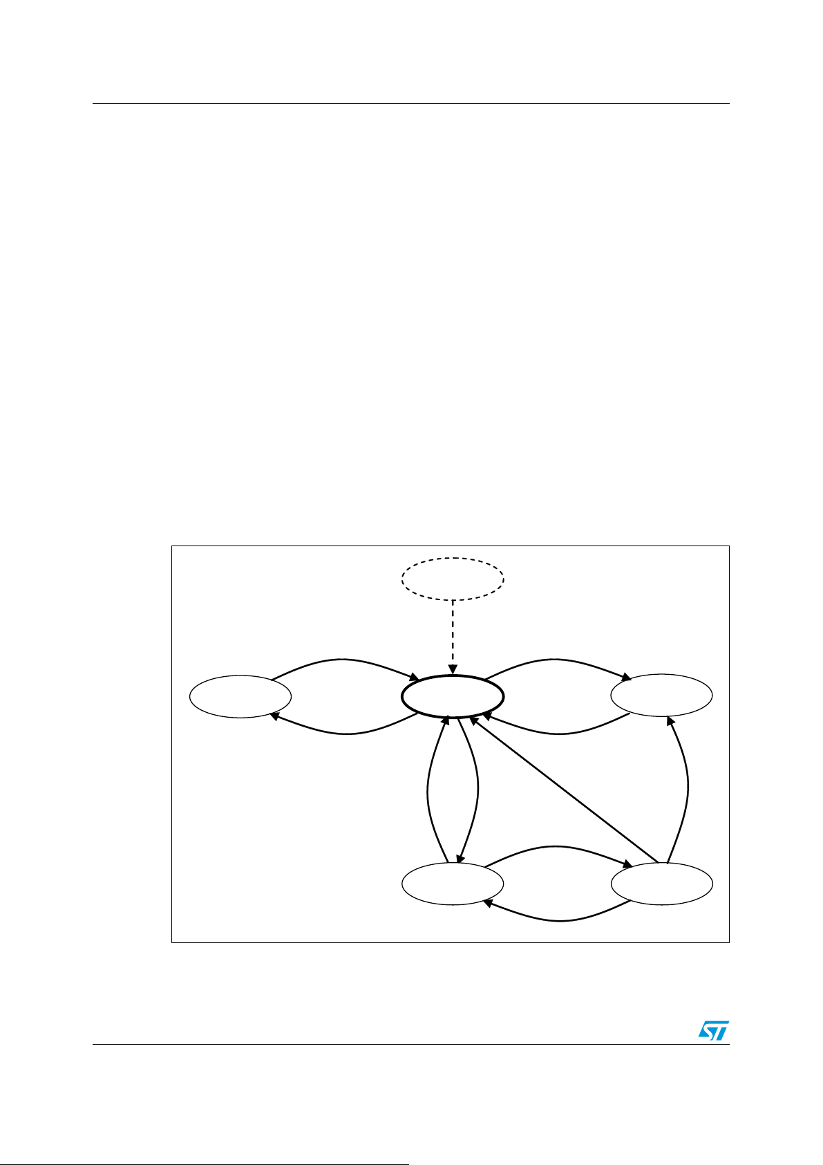
2%!$9
34!.$"9
3,%%0
2848,/#+
3(54$/7.
!-6
7 Operating modes
The SPIRIT1 is provided with a built-in main controller which controls the switching between
the two main operating modes: transmit (TX) and receive (RX).
In shutdown condition (the SPIRIT1 can be switched on/off with the external pin SDN, all
other functions/registers/commands are available through the SPI interface and GPIOs), no
internal supply is generated (in order to have minimum battery leakage), and hence, all
stored data and configurations are lost. From shutdown, the SPIRIT1 can be switched on
from the SDN pin and goes into READY state, which is the default, where the reference
signal from XO is available.
From READY state, the SPIRIT1 can be moved to LOCK state to generate the high
precision LO signal and/or TX or RX modes. Switching from RX to TX and vice versa can
happen only by passing through the LOCK state. This operation is normally managed by
radio control with a single user command (TX or RX). At the end of the operations above,
the SPIRIT1 can return to its default state (READY) and can then be put into a sleeping
condition (SLEEP state), having very low power consumption. If no timeout is required, the
SPIRIT1 can be moved from READY to STANDBY state, which has the lowest possible
current consumption while retaining FIFO, status and configuration registers. To manage the
transitions towards and between these operating modes, the controller works as a statemachine, whose state switching is driven by SPI commands. See Figure 3 for state diagram
and transition time between states.
Figure 3. Diagram and transition
The SPIRIT1 radio control has three stable states (READY, STANDBY, LOCK) which may be
defined stable, and they are accessed by the specific commands (respectively READY,
26/91 Doc ID 022758 Rev 2

SPIRIT1 Operating modes
STANDBY, and LOCKRX/LOCKTX), which can be left only if any other command is used. All
other states are transient, which means that, in a typical configuration, the controller
remains in those states, at most for any timeout timer duration. Also the READY and LOCK
states behave as transients when they are not directly accessed with the specific commands
(for example, when LOCK is temporarily used before reaching the TX or RX states).
Table 17. States
State/mode Digital LDO SPI Xtal RF Synth.
SHUTDOWN
STANDBY
SLEEP On Off Off On 350 µs 350 µs
READY (Default) On On Off Don’t care 110 µs 110 µs
LOCK On On On Don’t care NA NA
RX On On On Don’t care 20 µs NA
TX On On On Don’t care NA 20 µs
OFF (register
contents lost)
ON (FIFO and
register
contents
retained)
Off Off Off Off NA NA
On Off Off Off 320 µs 320 µs
Wake-up
timer
Response time to
TX RX
Note: Response time SHUTDOWN to READY is ~1 ms.
READY state is the default state after the power-on reset event. In the steady condition, the
XO is settled and usable as the time reference for RCO calibration, for frequency synthesis,
and as the system clock for the digital circuits.
The TX and RX modes can be activated directly by the MCU using the TX and RX
commands, or automatically if the state machine wakes up from SLEEP mode and some
previous TX or RX is pending.
(a)
In LOCK state the synthesizer is in a locking condition
. If LOCK state is reached using
either one of the two specific commands (LOCKTX or LOCKRX), the state machine remains
in LOCK state and waits for the next command. This feature can be used by the MCU to
perform preliminary calibrations, as the MCU can read the calibration word in the
RCO_VCO_CALIBR_OUT register and store it in a non-volatile memory, and after that it
requires a further tuning cycle.
When TX is activated by the TX command, the state machine goes into TX state and
remains there until the current packet is fully transmitted or, in the case of direct mode TX,
TXFIFO underflow condition is reached or the SABORT command is applied.
a. LOCK state is reached when one of the following events occurs first: lock detector assertion or locking timeout
expiration.
Doc ID 022758 Rev 2 27/91

Operating modes SPIRIT1
After TX completion, the possible destinations are:
● TX, if the persistent-TX option is enabled in the PROTOCOL configuration registers
● PROTOCOL, if some protocol option (e.g. automatic re-transmission) is enabled
● READY, if TX is completed and no protocol option is in progress.
Similarly, when RX is activated by the RX command, the state machine goes into RX state
and remains there until the packet is successfully received or the RX timeout expires. In
case of direct mode RX, the RX stops when the RXFIFO overflow condition is reached or
the SABORT command is applied. After RX completion, the possible destinations are:
● RX, if the persistent-RX option is enabled in the PROTOCOL configuration registers
● PROTOCOL, if some protocol option (e.g. automatic acknowledgement) is enabled
● READY, if RX is completed and the LDCR mode is not active
● SLEEP, if RX is completed and the LDCR mode is active.
The SABORT command can always be used in TX or RX state to break any deadlock
condition and the subsequent destination depends on SPIRIT1 programming according to
the description above.
Commands are used in the SPIRIT1 to change the operating mode, to enable/disable
functions, and so on. A command is sent on the SPI interface and may be followed by any
other SPI access without pulling CSn high.
The complete list of commands is reported in Ta bl e 18 . Note that the command code is the
second byte to be sent on the MOSI pin (the first byte must be 0x80).
Table 18. Commands list
Command
code
0x60 TX READY Start to transmit
0x61 RX READY Start to receive
0x62 READY
0x63 STANDBY READY Go to STANDBY
0x64 SLEEP READY Go to SLEEP
0x65 LOCKRX READY
0x66 LOCKTX READY
0x67 SABORT TX, RX Exit from TX or RX states and go to READY state
0x68 LDC_RELOAD All
0x69
Command name Execution state Description
SEQUENCE_UPDA
TE
STANDBY, SLEEP,
LOCK
All
Go to READY
Go to LOCK state by using the RX configuration of the
synthesizer
Go to LOCK state by using the TX configuration of the
synthesizer
Reload the LDC timer with the value stored in the
LDC_PRESCALER/COUNTER registers
Reload the packet sequence counter with the value
stored in the PROTOCOL[2] register.
0x6A AES Enc All Start the encryption routine
0x6B AES Key All Start the procedure to compute the key for decryption
0x6C AES Dec All Start decryption using the current key
28/91 Doc ID 022758 Rev 2
 Loading...