


LNB SUPPLY AND CONTROL VOLTAGE
REGULATOR (PARALLEL INTERFACE)
■ COMPLETE INTERFACE FOR TWO LNBs
REMOTE SUPPLY AND CONTROL
■ GUARANTEED 400mA OUTPUT CURRENT
■ LNB SELECTION AND STAND-BY
FUNCTION
■ BUILT-IN TONE OSCILLATOR FACTORY
TRIMMED AT 22KHz
■ FAST OSCILLATORSTART-UP FACILITATES
DiSEqC
■ TWO SUPPLY INPUTS FOR LOWEST
DISSIPATION
■ BYPASS FUNCTION FOR SLAVE
OPERATION
■ LNB SHORT CIRCUIT PROTECTION AND
DIAGNOSTIC
■ AUXILIARY MODULATIO N INPUT EXTENDS
FLEXIBILITY
■ CABLE LENGTH COMPENSATION
■ INTERNAL OVER TEMPERATURE
PROTECTION
■ BACKWARD CURRENT PROTECTION
■ COST-EFFECTIVE VERSION OF LNBP
SERIES
DESCRIPTION
Intended for analog and digital satellite receivers,
the LNBK20D2 is a monolithic linear voltage
regulator, assembled in SO-20, specifically
designed to provide the powering voltages and the
interfacing signals to the LNB downconverter
situated in the antenna via the coaxial c able. It has
the same functionality of the LNBP1X and
LNBP20 s eries, at a reduced output current
capability. Since most satellite receivers have two
antenna ports, the output voltage of the regulator
is av ailable at one of two logic-selectable output
pins (LNBA, LNBB). When the IC is powered and
put in Stand-by (EN pin LOW), both regulator
outputs are disabled to allow the antenna
downconverters to be supplied/controlled by
others satellite receivers s haring the s ame coaxial
lines. In this occurrence the device will limit at 3
mA (max) the backward current that could flow
from LNBA and LNBB output p ins t o GND.
For slave operation in single dish, dual receiver
systems, the bypass function is implemented by
an electronic switch between t he Master Input pin
ENCODING
LNBK20D2
SO-20
(MI) and the LNBA pin, thu s leaving all LNB
powering and control functions to the Master
Receiver. This electronic switch is c losed when
the device is powered and EN pin is LOW.
The r egulator outputs c an be logic controlled to be
13 or 18 V (typ.) by mean of the VSEL pin for
remote controlling of LNBs. Additionally, it is
possible to incr ement by 1V (typ.) the select ed
voltage value to compensate t he excess voltage
drop along th e coax ial cable (LLC pin HIGH).
In orde r to reduce the power dissipation of the
device when the l owes t output voltage is selected,
the regulator has two Supply Input pins V
V
. They must be powered res pectively at 16V
CC2
(min) and 23V (min), and an internal switch
automatically will select the suitable supply pin
according to the selected output voltage. If
adequate heatsink is provided and higher power
losses are acceptable, both su pply pins can be
powered by the sam e 23V source without
affecting any other circuit performance.
The ENT (T one Enable) pin activates the internal
oscillator so that the DC output is modulated by a
±0.3 V, 22KHz (typ.) square wave. This interna l
oscillator is factory trimmed within a tolerance of
±2KHz, thus no further adjustments neither
external components are required.
A burst coding of the 22KHz tone can be
accomplished thanks to the fast response of the
ENT i nput and the prompt oscillator start-up. This
helps designers who want to implement the
DiSEqC
protocols (*).
In order to improve design flexibility and to allow
implementation of newcoming LNB remote control
standards, an analogic modulation input pin is
CC1
and
1/14July 2003
LNBK20D2
available (EXTM). An appropriate DC blo cki ng
capacitor must be used to couple the m odulating
signal source to the EXTM pin. When external
modulation is not use d, the relevant pin can be left
open.
Two pins are dedicated to the overcurrent
protection/monitoring: CEXT and OLF. The
overcurrent protection circuit works dynamically:
as soon as an overload i s detected in either LNB
output, the output is shut-down for a time Toff
determined by the capacitor connec ted between
CEXT and GND. Simultaneously the OLF pin, t hat
is an open collector diagnostic output flag, from
HIGH IMPEDANCE state goes LOW.
After t he time has elapsed, the output is resumed
for a time t
(*): External components are needed to comply to level 2.x and above (bidirectiona) DiSEqCbus hardware requirements. DiSEqCis a
trademark or EUTELSAT.
=1/15t
on
(typ.) and OLF goes in HIGH
off
IMPEDANCE. If the overload is still present, the
protection circuit will cycle again through t
ton until the overload is removed. Typical t
and
off
on+toff
value is 1200ms when a 4.7µF external capacitor
is used.
This dynamic operation can greatly reduce the
power dissipation in short circuit condition, still
ensuring excellent power-on start up even with
highly capacitive loads on LNB outputs.
The device is packaged in Multiwatt15 for
thru-holes mou nting and in PowerSO-20 for
surface mounting. When a limited functionality in a
smaller package matches design needs, a range
of cost-effective PowerSO-10 solutions is also
offered. All version s have built-in thermal
protection agains t overheating damage.
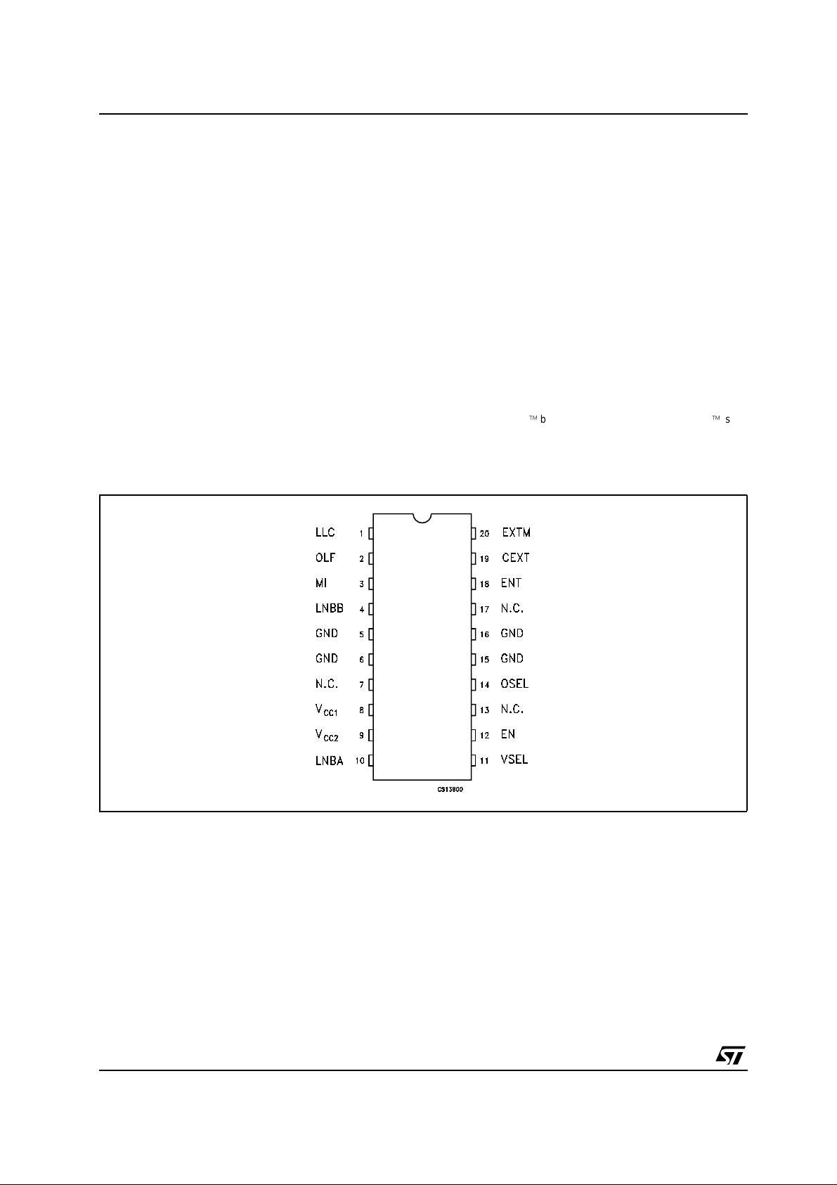
PIN CONFIGURA TION (top view)
2/14
LNBK20D2
TABLE A: PIN CONFIGURATIONS
PIN N° SYMBOL NAME FUNCTION
1 LLC Line Length Compens.
(1V typ)
2 OLF Over Load Flag Logic output (open collector). Normally in HIGH
3 MI Master Input In stand-by mode, the voltage on MI is routed to LNBA pin.
4 LNBB Output Port See truth tables for voltage and port selection
5, 6, 15,
GND Ground Circuit Ground. It is internally connected to the die frame
16
7, 13 N.C. Not Connected
8V
9V
CC1
CC2
Supply Input 1 15V to 27V supply. It is automatically selected when
Supply Input 2 22V to 27V supply. It is automatically selected when
10 LNBA Output Port See truth table voltage and port selection. In stand-by mode
11 V
SEL
Output Voltage Selection:
13 or 18V (typ)
12 EN Port Enable Logic control input: see truth table
14 OSEL Port Selection Logic control input: see truth table
18 ENT 22KHz Tone Enable Logic control input: see truth table
19 CEXT External Capacitor Timing Capacitor used by the Dynamic Overload protection.
20 EXTM External Modulator External Modulation Input. Needs DC decoupling to the AC
NOTE: the limited pin availability of the PowerSO-10 package leads to drop some f unctions.
Logic control input: see truth table
IMPEDANCE, goes LOW when current or thermal overload
occurs
Can be left open if bypass function is not needed
=13or14V
V
OUT
=18or19V
V
OUT
this port is powered by the MI pin via the internal Bypass
Switch
Logic control input: see truth table
Typical application is 4.7µF for a 1200ms cycle
source. if not used, can be left open.
ABSOLUTE MAXIMUM RATINGS
Symbol Parameter² Value Unit
V
I
V
I
SW
P
T
T
Absolute Maximum Ratings are those values beyond which damage to the device may occur. Functional operation under these condition is
not implied.
DC Input Voltage (V
I
Output Current (LNBA, LNBB)
O
Logic Input Voltage (ENT, EN OSEL, VSEL, LLC)
I
CC1,VCC2
, MI)
Bypass Switch Current
Power Dissipation at T
D
Storage Temperature Range
stg
Operating Junction Temperature Range
op
case
< 85°C
28 V
Internally Limited mA
-0.5 to 7 V
900 mA
3W
-40 to +150 °C
-40 to +125 °C
THERMAL DATA
Symbol Parameter Value Unit
R
thj-case
Thermal Resistance Junction-case
15 °C/W
3/14
LNBK20D2
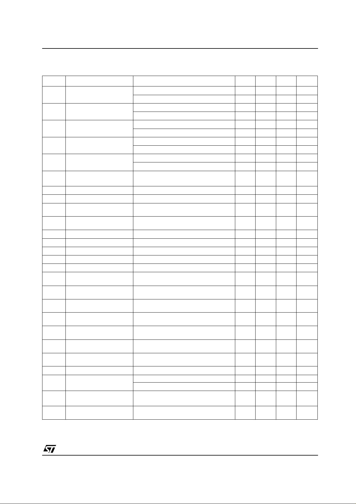
LOGIC CONTROLS TRUTH TABL E
CONTROL I/O PIN NAME L H
OUT OLF I
OUT>IOMAX
IN ENT 22KHz tone OFF 22KHz tone ON
IN EN See Table Below See Table Below
IN OSEL See Table Below See Table Below
IN VSEL See Table Below See Table Below
IN LLC See Table Below See Table Below
or Tj>150°C I
OUT<IOMAX
EN OSEL VSEL LLCO
LXXXV
V
LNBA
- 0.4V (typ.) Disabled
MI
H L L L 13V (typ.) Disabled
H L H L 18V (typ.) Disabled
H L L H 14V (typ.) Disabled
H L H H 19V (typ.) Disabled
H H L L Disabled 13V (typ.)
H H H L Disabled 18V (typ.)
H H L H Disabled 14V (typ.)
HHHH Disabled 19V (typ.)
NOTE: All logic input pins have internal pull-down resistor (typ. = 250KΩ)
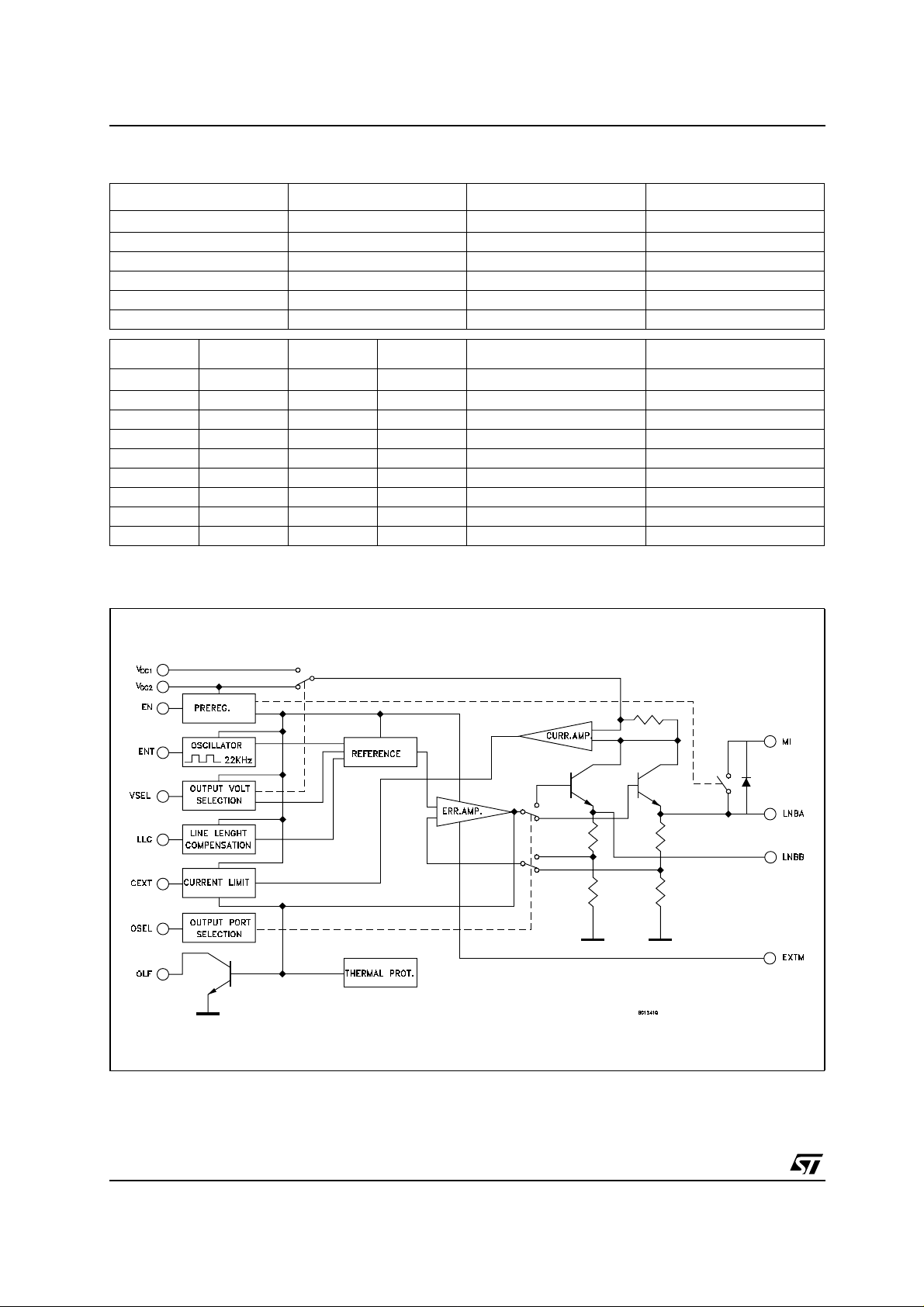
BLOCK DIAGRAM
V
LNBB
4/14
LNBK20D2
ELECTRICAL CHARACTERISTICS FOR LNBK SERIES (TJ= 0 to 85°C, CI=0.22µF, CO=0.1µF,
EN=H,ENT=L,LLC=L,V
Symbol Parameter Test Conditions Min. Typ. Max. Unit
V
IN1VCC1
V
IN2VCC2
V
O1
V
O2
∆V
O
∆V
O
SVR Supply Voltage Rejection V
I
MAX
t
OFF
t
ON
f
TONE
A
TONE
D
TONE
t
r,tf
G
EXTM
V
EXTM
Z
EXTM
V
SW
V
OL
I
OZ
V
IL
V
IH
I
IH
I
CC
I
OBK
T
SHDN
Supply Voltage IO= 400 mA ENT=H, VSEL=L, LLC=L 15 27 V
Supply Voltage IO= 400 mA ENT=H, VSEL=L, LLC=L 22 27 V
Output Voltage IO= 400 mA VSEL=L, LLC=L 17.3 18 18.7 V
Output Voltage IO= 400 mA VSEL=L, LLC=L 12.5 13 13.5 V
Line Regulation V
Load Regulation V
Output Current Limiting 500 650 800 mA
Dynamic Overload
protection OFF Time
Dynamic Overload
protection ON Time
Tone Frequency ENT=H 20 22 24 KHz
Tone Amplitude ENT=H 0.55 0.72 0.9 Vpp
Tone Duty Cycle ENT=H 40 50 60 %
Tone Rise and Fall Time ENT=H 5 10 15 µs
External Modulation Gain ∆V
External Modulation Input
Voltage
External Modulation
Impedance
Bypass Switch Voltage
Drop (MI to LNBA)
Overload Flag Pin Logic
LOW
Overload Flag Pin OFF
State Leakage Current
Control Input Pin Logic
LOW
Control Input Pin Logic
HIGH
Control Pins Input Current VIH=5V 20 µA
Supply Current Output Disabled (EN=L) 0.3 1 mA
Output Backward Current EN=L V
Temperature Shutdown
Threshold
=16V, V
IN1
=23V I
IN2
= 400 mA ENT=H, VSEL=L, LLC=H 16 27 V
I
O
= 400 mA VSEL=L, LLC=H 23 27 V
I
O
I
= 400 mA ENT=H, VSEL=L, LLC=H 19 V
O
= 400 mA ENT=H, VSEL=L, LLC=H 14 V
I
O
=15 to 18V V
IN1
=22 to 25V V
V
IN2
IN1=VIN2
=0to3A
I
O
IN1=VIN2
Output Shorted C
Output Shorted C
/∆V
OUT
=50mA, unless otherwise specified.)
OUT
=13V 5 50 mV
OUT
=18V 5 50 mV
OUT
=22V V
=13 or 18V
OUT
65 150 mV
=23± 0.5Vacfac= 120 Hz, 45 dB
=4.7µF 1100 ms
EXT
=4.7µFt
EXT
, f = 10Hz to 40KHz 5
EXTM
/15 ms
OFF
AC Coupling 400 mVpp
f = 10Hz to 40KHz 400 Ω
EN=L, ISW=300mA, V
CC2-VMI
=4V 0.35 0.6 V
IOL=8mA 0.28 0.5 V
VOH=6V 10 µA
0.8 V
2.5 V
ENT=H, I
V
IN1=VIN2
=500mA 3.1 6 mA
OUT
LNBA=VLNBB
= 18V
0.23mA
= 22V or floating
150 °C
5/14

LNBK20D2
TYPICAL CHARACTERISTICS
Figure1 : Output Voltage vs Output Current
Figure2 : T one Duty Cycle vs Temperature
(unless otherwise specified Tj= 25°C)
Figure4 : Tone Frequency vs Temperature
Figure5 : Tone Rise Time v s Temperature
Figure3 : Tone Fall Time vs Temperature
6/14
Figure6 : Tone Amplitude vs Temperature

LNBK20D2
Figure7 : S . V.R. v s Frequency
Figure8 : E x ternal Modulation vs Temperature
Figure10 : LNBA E x ternal Modulation gain vs
Frequency
Figure11 : Bypass switch Drop vs Output
Current
Figure9 : B y pas s Switch Drop vs Out put Current
Figure12 : overload Flag pin Logic LOW vs Flag
Current
7/14

LNBK20D2
Figure13 : Supply Vol tag e v s Temperature
Figure14 : Supply C urre nt vs Temperature
Figure16 : Tone E nable
Figure17 : Tone Disab le
Figure15 : Dynamic Overload protection (I
Time)
8/14
SC
vs
Figure18 : 22KHz T one

LNBK20D2
Figure19 : Enable Time
Figure20 : Disable Time
Figure21 : 18V to 13V Change
Figure22 : 18V to 13V Change
TYPICAL APPLICATION SCHEMATICS
TWO ANTENNA PORTS RECEIVER
10uF
10uF
C2
C2
11
AUX DA TA
AUX DA TA
47K
47K
R1
R1
11
EXTM
EXTM
13
13
OLF
OLF
4
4
VSEL
VSEL
9
9
ENT
ENT
5
5
EN
EN
7
7
OSEL
OSEL
12
12
LLC
LLC
LNBK20
LNBK20
I/OsVcc
I/OsVcc
1
1
VCC1
VCC1
2
2
VCC2
VCC2
3
3
LNBA
LNBA
15
15
LNBB
LNBB
14
14
MI
MI
10
10
CEXT
CEXT
4.7µF C4 C6C5
4.7µF C4 C6C5
8
8
GND
GND
MCU
MCU
17V 24VMCU+V
17V 24VMCU+V
ANT CONNECTORS
ANT CONNECTORS
JA
JA
JB
TUNER
TUNER
C1
C1
C3
C3
+
2x 47nF
2x 47nF
2x 0.1µF
2x 0.1µF
I/Os
I/Os
JB
9/14

LNBK20D2
SINGLE ANTENNA RECEIVER WITH MASTER RECEIVER PORT
24V17V
24V17V
C4 C5
C3
C4 C5
C3
47nF
47nF
AUX DATA
AUX DATA
MCU+V
MCU+V
R1
R1
47K
47K
10uF
10uF
C2
C2
11
11
EXTM
EXTM
13
13
OLF
OLF
4
4
VSEL
VSEL
9
9
ENT
ENT
5
5
EN
EN
7
7
OSEL
OSEL
12
12
LLC
LLC
LNBK20
LNBK20
I/OsVcc
I/OsVcc
VCC1
VCC1
VCC2
VCC2
LNBA
LNBA
LNBB
LNBB
CEXT
CEXT
GND
GND
1
1
2
2
3
3
15
15
14
14
MI
MI
10
10
4.7µF
4.7µF
C1
C1
+
8
8
MCU
MCU
2x 0.1µF
2x 0.1µF
TUNER
TUNER
I/Os
ANT
ANT
MASTER
MASTER
USING SERIAL BUS TO SAVE MPU I/Os
MCU+V
MCU+V
47K
47K
I/Os V cc
I/Os V cc
R1
R1
AUX DATA
AUX DATA
1
1
STR
STR
2
2
D
D
3
3
CLK
CLK
15
15
OE
OE
4094
4094
MCU+V
MCU+V
Q1
Q1
Q2
Q2
Q3
Q3
Q4
Q4
Q5
Q5
Q6
Q6
Q7
Q7
Q8
Q8
QS
QS
QS
QS
4
4
5
5
6
6
7
7
14
14
13
13
12
12
11
11
9
9
10
10
C2
C2
10uF
10uF
11
11
EXTM
EXTM
13
13
OLF
OLF
4
4
VSEL
VSEL
9
9
ENT
ENT
5
5
EN
EN
7
7
OSEL
OSEL
12
12
LLC
LLC
LNBK20
LNBK20
MCU
MCU
VCC1
VCC1
VCC2
VCC2
LNBA
LNBA
LNBB
LNBB
CEXT
CEXT
GND
GND
17V
17V
1
1
2
2
3
3
15
15
14
14
MI
MI
10
10
4.7µF
4.7µF
C1
C1
+
+
8
8
2x 0.1µF
2x 0.1µF
24V
ANT
ANT
CONNECTORS
CONNECTORS
JA
JA
JB
JB
TUNER
TUNER
C4 C6C5
C3
C4 C6C5
C3
2x 47nF
2x 47nF
SERIAL
SERIAL
BUS
BUS
10/14

LNBK20D2
THERMAL DESIGN NOTE
During normal operation, this de vice dissipates some power. At max imu m rated output c urrent (400mA),
the voltage drop on the linear regulator lead to a total dissipated power that is of about 2W . The heat
generated requires a suitable heatsink to keep the junction temperature below the over temperature
protection threshol d. Assuming a 40°C temperature inside the Set-Top-Box case, the total Rthj-amb has
to be less than 43°C/W.
While this can be easily achieved using a through-hole power package that can be attached to a small
heatsink or to the met allic frame of the receiver, a surface mount power package must rely on P C B
solutions whose thermal efficiency is oft en limited. The simplest solution is to use a large, continuous
copper area of the GND layer to dissipate the heat com ing from the IC body.
The SO -20 package of this IC has 4 GND pins that arenot just intended for electrical GND connection, but
also to prov ide a low thermal resistance path between the silicon chip and the PCB heatsink. Given an
Rthj-c equal to 15°C/W, a maximum of 28°C/W are left to the PCB heatsink. This figure is achieved if a
minimum of 25cm
a multi-layer PCB, or, in a dual layer PCB, an u nbrok en GND area even on the opposite side where the
IC is placed. In both cases, t he thermal path between the IC GND pins and the dissipating copper area
must exhibit a low thermal resistance.
In figure 4, it is shown a suggested layout for the SO-20 package with a dual layer PCB, where the IC
Ground pins and the sq uare dissipating area are thermally connec ted throug h 32 vias holes, filled by
solder. This arrangement, when L=50mm , achieves an Rthc-a of about 28°C/W.
Different layouts are possible, too. B as ic principles, however, suggest to keep the IC and its ground pins
approximately in the middle of the dissipating area; to provide as many vias as poss ible; to design a
dissipating area having a shape as square as poss ible and not interrupted by other copper trac es.
2
copper area is placed just below the IC body. This area can be the inner GND layer of
SO-20 SUGGESTED PCB HEATSINK L AYOUT
11/14

LNBK20D2
SO-20 MECHANICAL DATA
DIM.
MIN. TYP MAX. MIN. TYP. MAX.
A 2.65 0.104
a1 0.1 0.2 0.004 0.008
a2 2.45 0.096
b 0.35 0.49 0.014 0.019
b1 0.23 0.32 0.009 0.012
C 0.5 0.020
c1 45˚ (typ.)
D 12.60 13.00 0.496 0.512
E 10. 00 10.65 0.393 0.419
e 1.27 0.050
e3 11.43 0.450
F 7.40 7.60 0.291 0.300
L 0.50 1.27 0.020 0.050
M 0.75 0.029
S ˚ (max.)
mm. inch
8
12/14
PO13L

LNBK20D2
Tape & Reel SO-20 MECHANICAL DATA
mm. inch
DIM.
MIN. TYP MAX. MIN. TYP. MAX.
A 330 12.992
C 12.8 13.2 0.504 0.519
D 20.2 0.795
N 60 2.362
T 30.4 1.197
Ao 10.8 11 0.425 0.433
Bo 13.2 13.4 0.520 0.528
Ko 3.1 3.3 0.122 0.130
Po 3.9 4.1 0.153 0.161
P 11.9 12.1 0.468 0.476
13/14

LNBK20D2
Information furnished is believed to be accurate and reliable . However, STMicroelectronics assumes no responsibility for the
consequences of use o f suc h inf ormat ion n or f or an y infr ingeme nt of paten ts or oth er ri gh ts of third part ies whic h may resul t f rom
its use. No license is granted by implication or otherwise under any patent or patent rights of STMicroelectronics. Specifications
mentioned in this publication are subject to chang e without notice. This publication supersedes and replaces all information
previously supplied. STMicroelectronics products are not authorized for use as critical components in life support devices or
systems without express written approval of STMicroelectronics.
Australia - Brazil - Canada - China - Finland - France - Germany - Hong Kong - India - Israel - Italy - Japan - Malaysia - Malta - Morocco
© The ST logo is a registered trademark of STMicroelectronics
© 2003 STMicroelectronics - Printed in Italy - All Rights Reserved
STMicroelectronics GROUP OF COMPANIES
Singapore - Spain - Sweden - Switzerland - United Kingdom - United States.
© http://www.st.com
14/14
 Loading...