

LNBH24L
Dual LNBS supply and control IC with step-up and I²C interface
Features
■ Complete interface between LNBS and I²C bus
■ Built-in DC-DC converter for single 12 V supply
operation and high efficiency (typ. 93%@0.5 A)
■ Selectable output current limit by external
resistor
■ Compliant with main satellite receivers output
voltage specification
■ Auxiliary modulation input (EXTM) facilitates
DiSEqC™ 1.X encoding
■ Low-drop post regulator and high efficiency
step-up PWM with integrated power N-MOS
allow low power losses
■ Overload and over-temperature internal
protections with I²C diagnostic bits
■ Output voltage and output current level
diagnostic feedback by I²C bits
■ LNB short circuit dynamic protection
■ +/- 4 kV ESD tolerant on output power pins
QFN32 5 x 5 mm (ePad)
Description
Intended for analog and digital DUAL satellite
receivers/Sat-TV, Sat-PC cards, the LNBH24L is
a monolithic voltage regulator and interface IC,
assembled in QFN 5x5 ePAD, specifically
designed to provide the 13 / 18 V power supply
and the 22 kHz tone signaling for two independent
LNB down-converters in the antenna dishes
and/or multi-switch box. In this application field, it
offers a dual tuner STBs complete solution with
extremely low component count, low power
dissipation together with simple design and I²C
standard interfacing.
Table 1. Device summary
Order code Package Packaging
LNBH24LQTR QFN32 5 x 5 (Exposed pad) Tape and reel
March 2010 Doc ID 16857 Rev 2 1/25
www.st.com
25

Contents LNBH24L
Contents
1 Block diagram . . . . . . . . . . . . . . . . . . . . . . . . . . . . . . . . . . . . . . . . . . . . . . 4
2 Introduction . . . . . . . . . . . . . . . . . . . . . . . . . . . . . . . . . . . . . . . . . . . . . . . . 5
2.1 Application information (valid for each section A/B) . . . . . . . . . . . . . . . . . . 5
2.2 DiSEqC™ data encoding . . . . . . . . . . . . . . . . . . . . . . . . . . . . . . . . . . . . . . 5
2.3 DiSEqC™ 1.X implementation by EXTM pin . . . . . . . . . . . . . . . . . . . . . . . 5
2.4 DISEQC™ 1.X implementation with VoTX and EXTM pin connection . . . . 5
2.5 PDC optional circuit for DISEQC™ 1.X applications using
VoTX signal on to EXTM pin . . . . . . . . . . . . . . . . . . . . . . . . . . . . . . . . . . . 6
2.6 I²C interface . . . . . . . . . . . . . . . . . . . . . . . . . . . . . . . . . . . . . . . . . . . . . . . . 6
2.7 Output voltage selection . . . . . . . . . . . . . . . . . . . . . . . . . . . . . . . . . . . . . . . 6
2.8 Diagnostic and protection functions . . . . . . . . . . . . . . . . . . . . . . . . . . . . . . 6
2.9 Over-current and short circuit protection and diagnostic . . . . . . . . . . . . . . 7
2.10 Thermal protection and diagnostic . . . . . . . . . . . . . . . . . . . . . . . . . . . . . . . 7
2.11 Output current limit selection . . . . . . . . . . . . . . . . . . . . . . . . . . . . . . . . . . . 7
3 Pin configuration . . . . . . . . . . . . . . . . . . . . . . . . . . . . . . . . . . . . . . . . . . . 8
4 Maximum ratings . . . . . . . . . . . . . . . . . . . . . . . . . . . . . . . . . . . . . . . . . . . 10
5 Application circuits . . . . . . . . . . . . . . . . . . . . . . . . . . . . . . . . . . . . . . . . . 11
6 I²C bus interface . . . . . . . . . . . . . . . . . . . . . . . . . . . . . . . . . . . . . . . . . . . 13
6.1 Data validity . . . . . . . . . . . . . . . . . . . . . . . . . . . . . . . . . . . . . . . . . . . . . . . 13
6.2 Start and stop condition . . . . . . . . . . . . . . . . . . . . . . . . . . . . . . . . . . . . . . 13
6.3 Byte format . . . . . . . . . . . . . . . . . . . . . . . . . . . . . . . . . . . . . . . . . . . . . . . . 13
6.4 Acknowledge . . . . . . . . . . . . . . . . . . . . . . . . . . . . . . . . . . . . . . . . . . . . . . 13
6.5 Transmission without acknowledge . . . . . . . . . . . . . . . . . . . . . . . . . . . . . 13
7 LNBH24 software description . . . . . . . . . . . . . . . . . . . . . . . . . . . . . . . . 15
7.1 Interface protocol . . . . . . . . . . . . . . . . . . . . . . . . . . . . . . . . . . . . . . . . . . . 15
7.2 System register (SR, 1 Byte for each section A and B) . . . . . . . . . . . . . . 15
7.3 Transmitted data (I²C bus write mode) for each sections A/B . . . . . . . . . 15
2/25 Doc ID 16857 Rev 2

LNBH24L Contents
7.4 Diagnostic received data (I²C read mode) for both sections A/B . . . . . . . 16
7.5 Power-ON I²C interface reset . . . . . . . . . . . . . . . . . . . . . . . . . . . . . . . . . . 17
7.6 Address pins . . . . . . . . . . . . . . . . . . . . . . . . . . . . . . . . . . . . . . . . . . . . . . . 17
7.7 DiSEqC™ implementation for each section A/B . . . . . . . . . . . . . . . . . . . 17
8 Electrical characteristics . . . . . . . . . . . . . . . . . . . . . . . . . . . . . . . . . . . . 18
9 Package mechanical data . . . . . . . . . . . . . . . . . . . . . . . . . . . . . . . . . . . . 21
10 Revision history . . . . . . . . . . . . . . . . . . . . . . . . . . . . . . . . . . . . . . . . . . . 24
Doc ID 16857 Rev 2 3/25
Block diagram LNBH24L
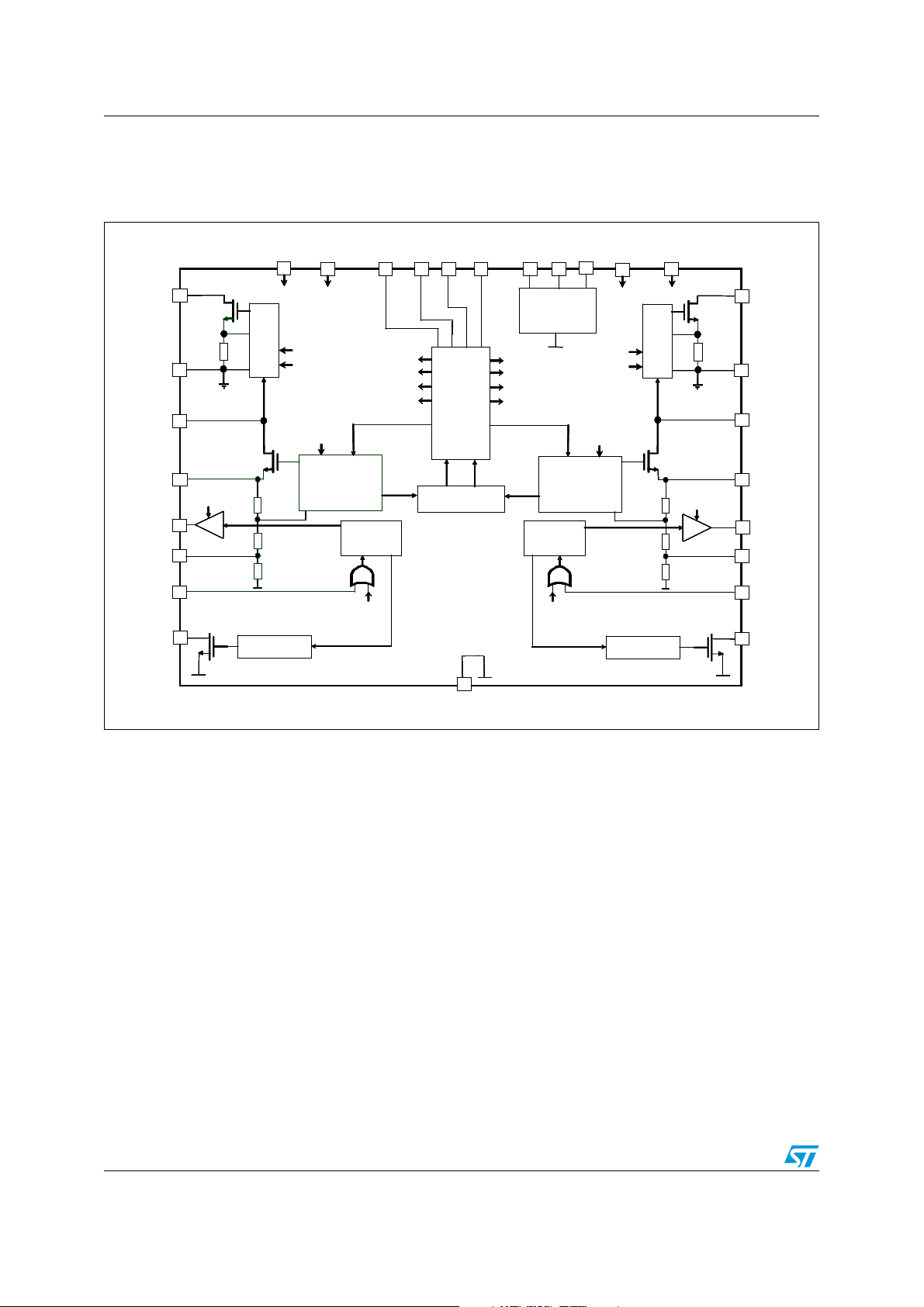
1 Block diagram
Figure 1. Block diagram
A
A
TTX-
TTX-
A
A
-
-
LX-
LX-
PWM
Rsense
Rsense
A
A
P-GND-
- -
P-GND-
- -
A
A
-
-
Vup -
Vup -
A
A
-
-
VoRX -
VoRX -
A
A
TTX-
TTX-
A
A
-
-
VoTX-
VoTX-
A
A
EXTM-
-
EXTM-
-
A
A
DSQIN-
-
DSQIN-
-
A
A
PDC
-
PDC
-
PWM
Controller
Controller
Pull Down
Pull Down
Controller
Controller
A
A
ISEL-
ISEL-
A
A
EN-
EN-
A
A
VSEL-
VSEL-
A
A
ISEL-
ISEL-
Linear Post-reg
Linear Post-reg
+Protections
+Protections
+Diagnostics
+Diagnostics
FB
FBFBFB
FB
FBFBFB
A
A
ADDR-
-
ADDR-
-
TEN-
TEN-
EN-
EN-
VSEL-
VSEL-
TTX-
TTX-
VOUT-AControl
-
VOUT-AControl
-
-
-
22 kHz
22 kHz
Oscillator
Oscillator
A
A
TEN-
TEN-
SDA SCL
SDA SCL
A
A
-
-
A
A
-
-
A
A
-
-
A
A
-
-
I²C Diagnostics
²
I²C Diagnostics
²
LNBH24L
LNBH24L
B
B
ADDR-
- -- - -
ADDR-
- -- - -
VOUT-BControl
VOUT-BControl
I²C interface
I
I²C interface
I
TEN-
TEN-
EN-
EN-
VSEL-
VSEL-
TTX-
TTX-
-
-
-
-
BypVcc
BypVcc
Preregulator
Preregulator
+U.V.lockout
+U.V.lockout
+P.ON reset
+P.ON reset
B
B
B
B
B
B
B
B
-
-
B
B
-
-
Linear Post-reg
Linear Post-reg
+Protections
+Protections
+Diagnostics
+Diagnostics
22 kHz
22 kHz
Oscillator
Oscillator
TEN-
TEN-
TEN-
TEN-
L
L
Vcc -
Vcc -
VSEL-
VSEL-
ISEL-
ISEL-
-
-
FB
FB
FB
FB
B
B
B
B
EN-
EN-
ISEL-
ISEL-
B
B
B
B
B
B
B
B
Pull Down
Pull Down
Controller
Controller
TTX-
TTX-
PWM
PWM
B
B
Rsense
Rsense
Rsense
Rsense
Controller
Controller
B
B
TTX-
TTX-
B
B
-
-
LX-
LX-
P-GND-
P-GND-
B
B
-
-
Vup -
Vup -
VoRX-
VoRX-
VoTX-
VoTX-
EXTM-
EXTM-
DSQIN-
DSQIN-
PDC
-
-
PDC
-
-
B
B
B
B
-
-
B
B
-
-
B
B
-
-
B
B
-
-
B
B
A-GND
A-GND
-
-
4/25 Doc ID 16857 Rev 2

LNBH24L Introduction
2 Introduction
The LNBH24L includes two completely independent sections. Unless for the VCC and I²C
inputs, each circuit can be separately controlled and have its independent external
components. All the below specification must be considered equal for both sections (A/B).
2.1 Application information (valid for each section A/B)
This IC has a built-in DC-DC step-up converter that, from a single source from 8 V to 15 V,
generates the voltages (V
dissipated power of 0.55 W typ. @ 500 mA load per channel (the linear post-regulator drop
voltage is internally kept at V
disable the whole circuit when the supplied V
typically).
) that let the linear post-regulator to work at a minimum
UP
UP
- V
= 1.1 V typ.). An under voltage lockout circuit will
OUT
drops below a fixed threshold (6.7 V
CC
Note: In this document the V
output (V
oRX
pin).
is intended as the voltage present at the linear post-regulator
OUT
2.2 DiSEqC™ data encoding
The new internal 22 kHz tone generator is factory trimmed in accordance to the standards,
and can be selected by I²C interface TTX bit (or TTX pin) and activated by a dedicated pin
(DSQIN) that allows immediate DiSEqC™ data encoding, or through TEN I²C bit in case the
22 kHz presence is requested in continuous mode. In stand-by condition (EN bit LOW) the
TTX function must be disabled setting TTX to LOW.
2.3 DiSEqC™ 1.X implementation by EXTM pin
In order to improve design flexibility and reduce the total application cost, an analogic
modulation input pin is available (EXTM) to generate the 22 kHz tone superimposed to the
V
DC output voltage. An appropriate DC blocking capacitor must be used to couple the
oRX
modulating signal source to the EXTM pin. If the EXTM solution is used the output R-L filter
can be removed (see Section 5: Application circuits) saving the external components
cost.The pin EXTM modulates the V
that:
voltage through the series decoupling capacitor, so
oRX
GVV ×=
)AC(EXTM)AC(oRX
EXTM
Where V
(AC) and V
oRX
and EXTM pins while G
(AC) are, respectively, the peak to peak voltage on the V
EXTM
is the voltage gain from EXTM to V
EXTM
2.4 DISEQC™ 1.X implementation with V
connection
If an external 22 kHz tone source is not available, it is possible to use the internal 22 kHz
tone generator signal available through the V
Doc ID 16857 Rev 2 5/25
pin to drive the EXTM pin. By this way the
oTX
.
oRX
and EXTM pin
oTX
oRX

Introduction LNBH24L
V
22 kHz signal will be superimposed to the V
oTX
22 kHz tone (see
internal 22 kHz tone generator available through the V
22 kHz transmission by DSQIN pin or by the TEN bit.The DSQIN internal circuit activates
the 22 kHz tone on the V
presence on the DSQIN pin, and it stops with 1 cycles ± 25 µs delay after the TTL signal is
expired. The V
can be controlled both through the TTX pin and by I²C bit. As soon as the tone transmission
is expired, the V
supply is always provided to the LNB from the V
Figure 3: LNBH24L with internal tone for DiSEqC 1.X applications). The
output with 0.5 cycles ± 25 µs delay from the TTL signal
oTX
pin internal circuit must be preventively set ON by the TTX function. This
oTX
must be disabled by setting the TTX to LOW. The 13 / 18 V power
oTX
DC voltage to generate the LNB output
oRX
pin must be activated during the
oTX
pin.
oRX
2.5 PDC optional circuit for DISEQC™ 1.X applications using
V
signal on to EXTM pin
oTX
In some applications, at light output current (< 50 mA) and in case of heavy output
capacitive load, the 22 kHz tone can be distorted. In this case it is possible to add the
"Optional" external components shown in the typical application circuit (see
DiSEqC 1.x using external 22 kHz tone generator source through EXTM pin
between V
output capacitance only when the internal 22 kHz tone is activated.
and PDC pin. This optional circuit acts as an active pull-down discharging the
oRX
Figure 4:
) connected
2.6 I²C interface
The main functions of the IC are controlled via I²C bus by writing 6 bits on the system
register (SR 8 bits in write mode). On the same register there are 5 bits that can be read
back (SR 8 bits in read mode) to provide the diagnostic flags of two internal monitoring
functions (OTF, OLF) and three output voltage register status (EN, VSEL, LLC) received by
the IC (see
bits (TEST1-2-3) that must be disregarded from the MCU. While, in write mode, there 2 Test
bits (TEST4-5) that must be always set LOW. Each section (A/B) has two selectable I²C
addresses selectable respectively, by the ADDR-A and ADDR-B pins (see
Address pins characteristics
Section 2.8: Diagnostic and protection functions). In read mode there are 3 test
).
2.7 Output voltage selection
When the IC sections are in stand-by mode (EN bit LOW), the power blocks are disabled.
When the regulator blocks are active (EN bit HIGH), the output can be logic controlled to be
13 or 18 V by mean of the VSEL bit (voltage SELect) for remote controlling of non-DiSEqC
LNBs. Additionally, the LNBH24L is provided with the LLC I²C bit that increase the selected
voltage value to compensate possible voltage drop along the output line. In stand-by
condition (EN bit LOW) all the I²C bits and the TTX pin must be set LOW (if the TTX pin is
not used it can be left floating but the TTX bit must be set LOW during the stand-by
condition).
Ta bl e 11 :
2.8 Diagnostic and protection functions
The LNBH24L has two diagnostic internal functions provided via I²C bus by reading 2 bits on
the system register (SR bits in read mode). The diagnostic bits are, in normal operation (no
6/25 Doc ID 16857 Rev 2

LNBH24L Introduction
failure detected), set to LOW. The diagnostic bits are dedicated to the over-temperature and
over-load protections status (OTF and OLF).
2.9 Over-current and short circuit protection and diagnostic
In order to reduce the total power dissipation during an overload or a short circuit condition,
the device is provided with a dynamic short circuit protection. It is possible to set the short
circuit current protection either statically (simple current clamp) or dynamically by the PCL
bit of the I²C SR. When the PCL (pulsed current limiting) bit is set lo LOW, the over current
protection circuit works dynamically: as soon as an overload is detected, the output is shutdown for a time T
system register is set to "1". After this time has elapsed, the output is resumed for a time
= 1/10 T
T
ON
OFF
protection circuit will cycle again through T
overload is detected, normal operation is resumed and the OLF diagnostic bit is reset to
LOW. Typical T
operation can greatly reduce the power dissipation in short circuit condition, still ensuring
excellent power-on start-up in most conditions. However, there could be some cases in
which a highly capacitive load on the output may cause a difficult start-up when the dynamic
protection is chosen. This can be solved by initiating any power start-up in static mode
(PCL=1) and, then, switching to the dynamic mode (PCL=0) after a chosen amount of time
depending on the output capacitance. When in static mode, the diagnostic OLF bit goes to
"1" when the current clamp limit is reached and returns LOW when the overload condition is
cleared.
, typically 900 ms. Simultaneously the diagnostic OLF I²C bit of the
OFF
= 90 ms (typ.). At the end of TON, if the overload is still detected, the
and TON. At the end of a full TON in which no
OFF
ON
+ T
time is 990 ms and an internal timer determines it. This dynamic
OFF
2.10 Thermal protection and diagnostic
The LNBH24L is also protected against overheating: when the junction temperature
exceeds 150°C (typ.), the step-up converter and the liner regulator are shut-off, and the
diagnostic OTF SR bit is set to "1". Normal operation is resumed and the OTF bit is reset to
LOW when the junction is cooled down to 135°C (typ.)
2.11 Output current limit selection
The linear regulator current limit threshold can be set by an external resistor connected to
ISEL pin. The resistor value defines the output current limit by the equation:
Equation 1
10000
10000
=
=
[A]I
[A]I
MAX
MAX
where R
is the resistor connected between I
SEL
application circuit). The highest selectable current limit threshold is 0.9 A typ. with R
Ω. The above equation defines the typical threshold value for each output. However, it is
k
suggestible to not exceed for a long period a total amount of current of 1 A from both
sections (I
OUT_A
+ I
< 1 A) in order to avoid the over temperature protection triggering.
OUT_B
Note: External components are needed to comply to bidirectional DiSEqC™ bus hardware
requirements. Full compliance of the whole application with DiSEqC™ specifications is not
implied by the bare use of this IC. NOTICE: DiSEqC™ is a trademark of EUTELSAT.
R
R
SEL
SEL
and GND (see R2 in the typical
SEL
SEL
= 11
Doc ID 16857 Rev 2 7/25
Pin configuration LNBH24L
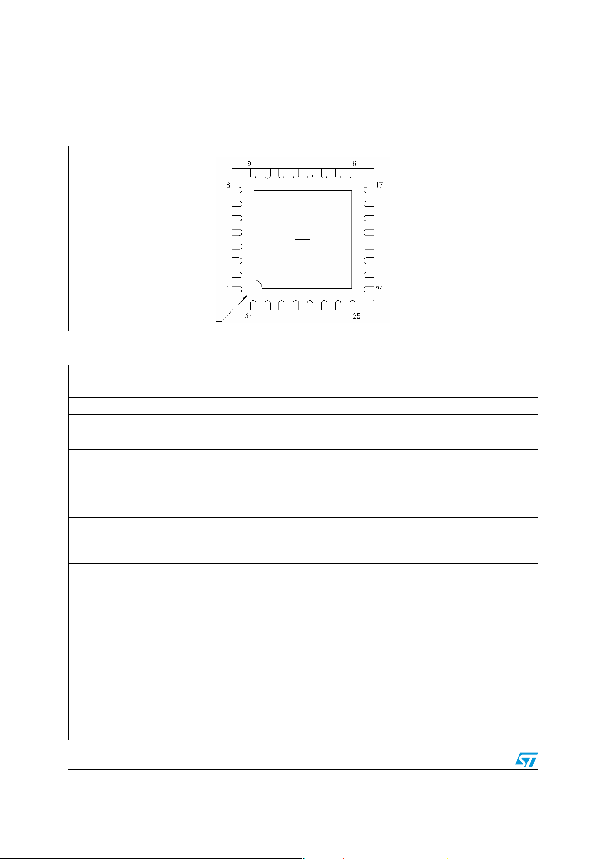
3 Pin configuration
Figure 2. Pin connections (bottom view)
Table 2. Pin description
Pin n°
(sec. A/B)
21 V
20 V
Symbol Name Pin function
CC
L Supply Input 8 to 15 V analog power supply.
CC–
Supply Input 8 to 15 V IC DC-DC power supply.
5 / 2 LX-A / LX-B N-MOS Drain Integrated N-channel Power MOSFETs drain.
16 /
25
18 /
23
17 /
24
V
UP
VUP-B
V
oRX
V
oRX
V
oTX –
V
oTX –
-A /
-A /
-B
A /
Step-Up Voltage
LDO Output Port
Output Port during
B
22KHz Tone TX
Input of the linear post-regulators. The voltage on these pins is
monitored by the internal step-up controllers to keep a
minimum dropout across the linear pass transistors.
Outputs of the integrated low drop linear regulators. See
Ta bl e 7 for voltage selections and description.
Tone outputs to the LNB. See Ta b le 7 for selection.
6 SDA Serial Data Bidirectional data from / to I²C bus.
7 SCL Serial Clock Clock from I²C bus.
These pins will accept the DiSEqC code from the main
10 /
31
DSQIN-A /
DSQIN-B
DiSEqC Inputs
microcontroller. The LNBH24L will uses this code to modulate
the internally generated 22 kHz carrier. Set to ground if not
used.
These pins can be used, as well as the TTX I²C bits of the
12 /
29
TTX-A /
TTX-B
TTX Enable
system register, to control the TTX function enable before to
start the 22 kHz tone transmission. Set floating or to GND if
not used.
11 / 30 Reserved Reserved To be connected to GND.
9 /
32
PDC – A /
PDC – B
Pull Down Control
To be connected to the external NPN transistors base to
reduce the 22 kHz tone distortion in case of heavy capacitive
load at light output current. If not used they can be left floating.
8/25 Doc ID 16857 Rev 2
 Loading...