

ST LMX321, LMX358, LMX324 User Manual
General-purpose, low voltage rail-to-rail output operational
Features
■ Low power consumption: 120 µA at 2.7 V
■ Low supply voltage: 2.3 V - 5.5 V
■ Rail to rail output swing
■ Gain bandwidth product: 1.3 MHz
■ Extended temperature range: -40°C to +125°C
■ No crossover distortion
■ No phase reversal
■ Tiny packages
Related products
■ See TSV85x series for higher accuracy, stand-
by options and smaller packages
LMX321, LMX358, LMX324
amplifiers
Datasheet − production data
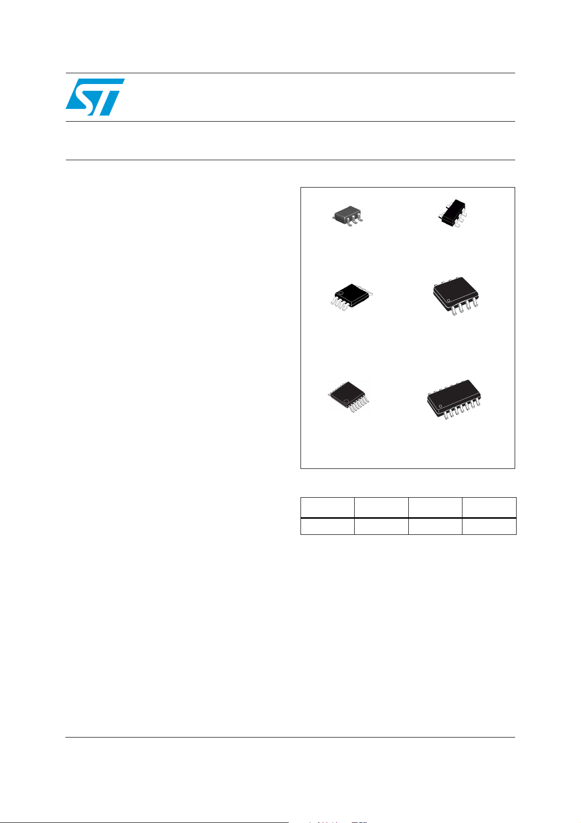
SC70-5
MiniSO-8
SOT23-5
SO-8
Applications
■ Battery-powered applications
■ Portable devices
■ Signal conditioning
■ Active filtering
■ Medical instrumentation
Description
The LMX3xx series is a set of single, dual and
quad low-voltage, general-purpose operational
amplifiers. These devices can operate from 2.3 V
to 5.5 V with a typical current consumption of
120 μA per channel. The LMX3xx series offers a
rail-to-rail output and an input common-mode
voltage that includes ground.
The LMX3xx series also exhibits a 1.3 MHz gain
bandwidth and can drive capacitive loads. The
devices are stable while operating at unity gain.
They are offered with industry standard pinouts in
tiny packages.
TSSOP14
SO-14
Table 1. Device summary
Reference Single Dual Quad
LMX3xx LMX321 LMX358 LMX324
April 2012 Doc ID 022943 Rev 2 1/21
This is information on a product in full production.
www.st.com
21
Package pin connections LMX321, LMX358, LMX324
5
2
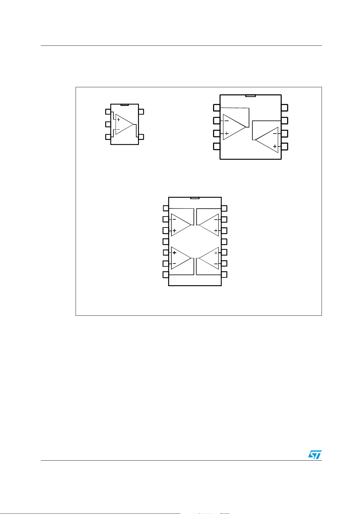
1 Package pin connections
Figure 1. Pin connections for each package (top view)
1
In+
Vcc-
2
In- Out
3
5
4
SC70-5 / SOT23-5
Vcc+
Out1
In1-
In1+
In2+
In2-
Out
Out1
In1-
In1+
1
2
3
4Vcc-
Vcc+
8
Out2
7
In2-
6
5In2+
SO-8 / MiniSO-8
1
2
3
4Vcc+
6
7
14
Out4
13
In4-
In4+
12
11
Vcc-
10
In3+
In3-
9
8
Out3
TSSOP-14 / SO-14
2/21 Doc ID 022943 Rev 2
LMX321, LMX358, LMX324 Absolute maximum ratings and operating conditions
2 Absolute maximum ratings and operating conditions
Table 2. Absolute maximum ratings (AMR)
Symbol Parameter Value Unit
(4)
(1)
(8)
(2)
(7)
(9)
(3)
(5)(6)
V
cc-
6V
±V
CC
- 0.3 to V
+ 0.3 V
cc+
V
10 mA
°C/W
4000
250
VMM: machine model
1300
V
CC
V
V
I
in
T
stg
Supply voltage
Differential input voltage
id
Input pins (IN+ and IN- pins) voltage
in
Input current
Storage temperature -65 to +150 °C
Thermal resistance junction to ambient
SC70-5 205
SOT23-5 250
R
thja
MiniSO8 190
SO8 125
TSSOP14 100
SO14 105
T
Maximum junction temperature 150 °C
j
HBM: human body model
ESD
CDM: charged device model
Latch-up immunity 200 mA
1. All voltage values, except differential voltage, are with respect to network ground terminal.
2. Differential voltages are the non-inverting input terminal with respect to the inverting input terminal.
3. VCC-Vin must not exceed 6 V, Vin must not exceed 6 V.
4. Input current must be limited by a resistor in series with the inputs.
5. Short-circuits can cause excessive heating and destructive dissipation.
6. R
are typical values.
th
7. Human body model: 100 pF discharged through a 1.5 kΩ resistor between two pins of the device, done for
all couples of pin combinations with other pins floating.
8. Machine model: a 200 pF cap is charged to the specified voltage, then discharged directly between two
pins of the device with no external series resistor (internal resistor < 5 Ω), done for all couples of pin
combinations with other pins floating.
9. Charged device model: all pins plus package are charged together to the specified voltage and then
discharged directly to the ground.
Table 3. Operating conditions
Symbol Parameter Value Unit
T
V
V
CC
icm
oper
Supply voltage 2.3 to 5.5 V
Common mode input voltage range V
CC-
- 0.2 to V
- 1 V
CC+
Operating free air temperature range -40 to +125 °C
Doc ID 022943 Rev 2 3/21
Electrical characteristics LMX321, LMX358, LMX324
3 Electrical characteristics
Table 4. Electrical characteristics at V
Symbol Parameter Conditions Min. Typ. Max. Unit
DC performance
and R
= 2.7 V with V
connected to VCC/2 (unless otherwise specified)
L
CC+
= 0 V, V
CC-
= VCC/2, T
icm
= 25° C,
amb
V
ΔV
io
I
I
CMR
A
V
CC-VOH
V
I
out
Input offset voltage
io
/ΔT Input offset voltage drift
Input offset current
io
Input bias current
ib
Common mode rejection ratio
20 log (ΔV
Large signal voltage gain
vd
icm
High level output voltage
Low level output voltage
OL
I
sink
I
source
/ΔVio)
(1)
4
mV
-40°C < T< 125°C 6
-40°C < T< 125°C 1 μV/°C
V
out=Vcc
/2 0.5 30
nA
-40°C < T< 125°C 50
V
out=Vcc
/2 27 60
nA
-40°C < T< 125°C 110
V
ic = 0 V to V
V
= V
out
-1 V,
cc
/2
cc
70 75
dB
-40°C < T< 125°C 68
= 10 kΩ,
R
L
V
= 0.5 V to (Vcc-0.5 V)
out
100 110
-40°C < T< 125°C 90
dB
RL= 2 kΩ,
V
= 0.5 V to (Vcc-0.5 V)
out
90 100
-40°C < T< 125°C 80
=10kΩ, 10 100
R
L
-40°C < T< 125°C 200
mV
R
=2kΩ 40 300
L
-40°C < T< 125°C 400
=10kΩ, 65 180
R
L
-40°C < T< 125°C 280
mV
R
=2kΩ, 120 300
L
-40°C < T< 125°C 400
V
= Vcc, Vid = -1 V 15 26
out
mA
-40°C < T< 125°C 15
V
= 0 V, Vid = 1 V 15 21
out
mA
-40°C < T< 125°C 12
I
CC
Supply current (per channel)
-40°C < T< 125°C 180
No load, V
= VCC/2 120 180
out
4/21 Doc ID 022943 Rev 2
µA
LMX321, LMX358, LMX324 Electrical characteristics
A
Table 4. Electrical characteristics at V
and R
connected to VCC/2 (unless otherwise specified) (continued)
L
= 2.7 V with V
CC+
= 0 V, V
CC-
= VCC/2, T
icm
= 25° C,
amb
Symbol Parameter Conditions Min. Typ. Max. Unit
AC performance
GBP Gain bandwidth product R
F
Φ
G
Unity gain frequency RL>1MΩ, CL= 200 pF 1 MHz
u
Phase margin RL>1MΩ, CL= 200 pF 60 degrees
m
Gain margin RL>1MΩ, CL= 200 pF 10 dB
m
SR Slew rate
e
i
Equivalent input noise voltage
n
Equivalent input noise current f = 1 kHz 0.30
n
THD+N Total harmonic distortion + noise
Table 5. Electrical characteristics at V
connected to VCC/2 (unless otherwise specified)
R
L
>1MΩ, CL= 200 pF 1.3 MHz
L
R
>1MΩ, CL= 200 pF
L
V
= 0.5 V to VCC-0.5V
out
f=1kHz
f = 10 kHz
= 1 kHz, A
f
in
CL
= 1,
RL = 10 kΩ,
= VCC/2, BW = 22 kHz,
V
ICM
V
= 1 Vpp
out
= 5 V with V
CC+
= 0 V, V
CC-
icm
0.6 V/μs
31
20
0.002 %
= VCC/2, T
amb
= 25° C, and
Symbol Parameter Conditions Min. Typ. Max. Unit
nV
-----------Hz
p
-----------Hz
DC performance
ΔV
CMR
SVR
V
io
I
I
A
Input offset voltage
io
/ΔT Input offset voltage drift
Input offset current
io
Input bias current
ib
Common mode rejection ratio
20 log (ΔV
Supply voltage rejection ratio
20 log (ΔV
Large signal voltage gain
vd
icm
cc
/ΔVio)
/ΔVio)
(1)
4
mV
-40°C < T< 125°C 6
-40°C < T< 125°C 1 μV/°C
V
out=Vcc
/2 0.5 30
nA
-40°C < T< 125°C 50
V
out=Vcc
/2 27 60
nA
-40°C < T< 125°C 110
V
ic = 0 V to V
V
= V
out
-1V,
cc
/2
cc
72 75
dB
-40°C < T< 125°C 70
= 2.5 to 5 V 72 79
V
cc
dB
-40°C < T< 125°C 70
RL= 10 kΩ,
V
= 0.5 V to (V
out
CC
- 0.5 V)
-40°C < T< 125°C 90
100 110
dB
RL=2kΩ, 90 100
-40°C < T< 125°C 80
Doc ID 022943 Rev 2 5/21
Electrical characteristics LMX321, LMX358, LMX324
A
Table 5. Electrical characteristics at V
connected to VCC/2 (unless otherwise specified) (continued)
R
L
= 5 V with V
CC+
= 0 V, V
CC-
= VCC/2, T
icm
= 25° C, and
amb
Symbol Parameter Conditions Min. Typ. Max. Unit
=10kΩ 10 100
R
L
-40°C < T< 125°C 200
VCC-VOHHigh level output voltage
RL=2kΩ, 40 300
-40°C < T< 125°C 400
=10kΩ 65 180
R
L
-40°C < T< 125°C 280
V
Low level output voltage
OL
R
=2kΩ 120 300
L
-40°C < T< 125°C 400
V
= VCC, Vid = -1 V 35 43
I
sink
I
out
I
source
I
CC
Supply current (per channel)
out
-40°C < T< 125°C 25
V
= 0 V, Vid = 1 V 60 70
out
-40°C < T< 125°C 50
No load, V
= VCC/2 130 180
out
-40°C < T< 125°C 180
AC performance
mV
mV
mA
mA
µA
GBP Gain bandwidth product R
F
Φ
G
Unity gain frequency RL>1MΩ, CL= 200 pF 1 MHz
u
Phase margin RL>1MΩ, CL= 200 pF 60 degrees
m
Gain margin RL>1MΩ, CL= 200 pF 10 dB
m
SR Slew rate
e
i
Equivalent input noise voltage
n
Equivalent input noise current f = 1 kHz 0.30
n
THD+N Total harmonic distortion + noise
1. See Chapter 4.4: Input offset voltage drift over temperature.
>1MΩ, CL= 200 pF 1.3 MHz
L
R
>1MΩ, CL= 200 pF
L
V
= 0.5 V to VCC-0.5V
out
f=1kHz
f=10kHz
= 1 kHz, A
f
in
R
= 10 kΩ,
L
= VCC/2, BW = 22 kHz,
V
ICM
= 1 Vpp
V
out
CL
= 1,
0.7 V/μs
30
20
nV
------------
p
------------
0.002 %
Hz
Hz
6/21 Doc ID 022943 Rev 2
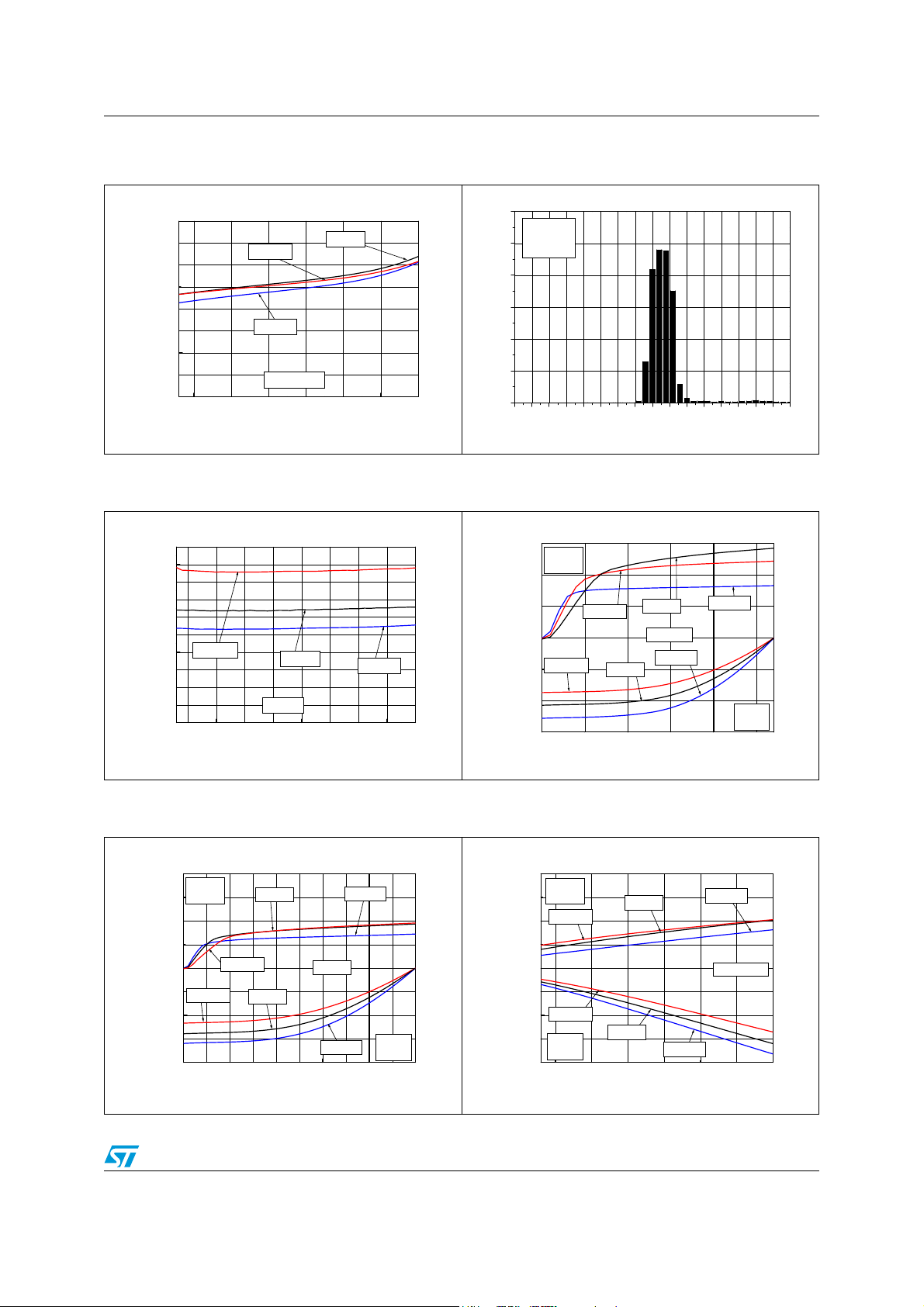
LMX321, LMX358, LMX324 Electrical characteristics
Figure 2. Supply current vs. supply voltage at
V
= VCC/2
icm
0.20
0.15
0.10
Supply Current (mA)
0.05
0.00
2.5 3.0 3.5 4.0 4.5 5.0 5.5
T=125°C
T=-40°C
Vicm=Vcc/2
Supply Voltage (V)
T=25°C
Figure 4. Input offset voltage vs. input
common mode voltage at V
1.0
0.9
0.8
0.7
0.6
0.5
T=125°C
0.4
0.3
0.2
Input Offset Vol tage (mV)
0.1
0.0
0.0 0.5 1.0 1.5 2.0 2.5 3.0 3.5 4.0
Input Common Mode Voltage (V)
T=25°C
Vcc=5V
T=-40°C
CC
= 5 V
Figure 3. Vio distribution at VCC = 5 V
30
Vcc=5V
Vicm=2.5V
25
T=25°C
20
15
10
Population (%)
5
0
-4.0 -3.5 -3.0 -2.5 -2.0 -1.5 -1.0 -0.5 0.0 0.5 1.0 1.5 2.0 2.5 3.0 3.5 4.0
Input offset voltage (mV)
Figure 5. Output current vs. output voltage at
VCC = 2.7 V
30
Sink
Vid=-1V
2020
10
00
-10
Output Current (mA)
-20-20
-30
0.00.0 0.5 1.01.0 1.5 2.02.0 2.5
T=125°C
T=125°C
T=25°C
Vcc=2.7V
T=25°C
T=-40°C
Output Voltage (V)
T=-40°C
Source
Vid=1V
Figure 6. Output current vs. output voltage at
= 5 V
V
CC
100100
Sink
75
Vid=-1V
5050
25
00
-25
T=125°C
Output Current (mA)
-50-50
-75
-100-100
0.00.0 0.5 1.01.0 1.5 2.02.0 2.5 3.03.0 3.5 4.04.0 4.5 5.05.0
T=25°C
T=125°C
T=25°C
Output Voltage (V)
Vcc=5V
T=-40°C
T=-40°C
Source
Vid=1V
Doc ID 022943 Rev 2 7/21
Figure 7. Output current vs. supply voltage at
V
= VCC/2
icm
100100
Sink
75
Vid=-1V
T=125°C
5050
25
00
-25
Output Current (mA)
-50-50
T=125°C
-75
Source
Vid=1V
-100-100
2.5 3.03.0 3.5 4.04.0 4.5 5.05.0 5.5
T=25°C
T=25°C
Supply Voltage (V)
T=-40°C
Vicm=Vcc/2
T=-40°C
 Loading...