


LMV82x, LMV82xA
Low power, high accuracy, general-purpose operational amplifier
Features
■ Low power consumption: 400 µA max at 5 V
■ Low power shutdown mode: 50 nA max
■ Low offset voltage: 0.8 mV max at 25°C
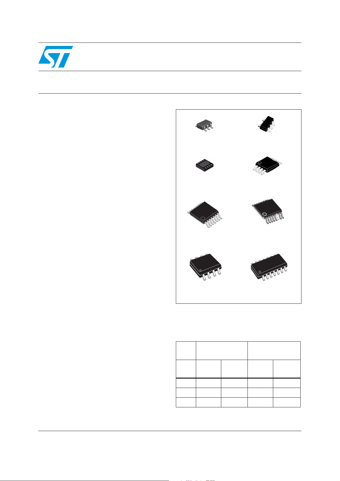
■ Tiny packages
■ Extended temperature range: -40°C to +125°C
■ Low supply voltage: 2.5 V - 5.5 V
■ Gain bandwidth product: 5.5 MHz
Benefits
■ Longer lifetime in battery-powered applications
■ Higher accuracy without calibration
■ Smaller form factor than equivalent competitor
devices
■ Application performances guaranteed over
wide temperature range
SC70-5
DFN8 2x2
TSSOP14
SOT23-5 / SOT23-6
MiniSO8 / MiniSO10
TSSOP16
Related products
■ See TSV85x series for lower power
consumption (180 µA max at 5 V)
Applications
■ Battery-powered applications
■ Portable devices
■ Signal conditioning
■ Active filtering
■ Medical instrumentation
Description
The LMV82x series of single, dual and quad
operational amplifiers offers low voltage operation
with rail-to-rail output swing. The LMV82x series
outperforms the industry standard LMV321
especially with regard to the gain bandwidth
product (5.5 MHz). The LMV821, LMV822 and
LMV824 are proposed with standard pinouts.
SO8
SO14
The LMV820, LMV823 and LMV825 include a
power-saving shutdown feature that reduces the
supply current to a maximum of 50 nA at 25°C.
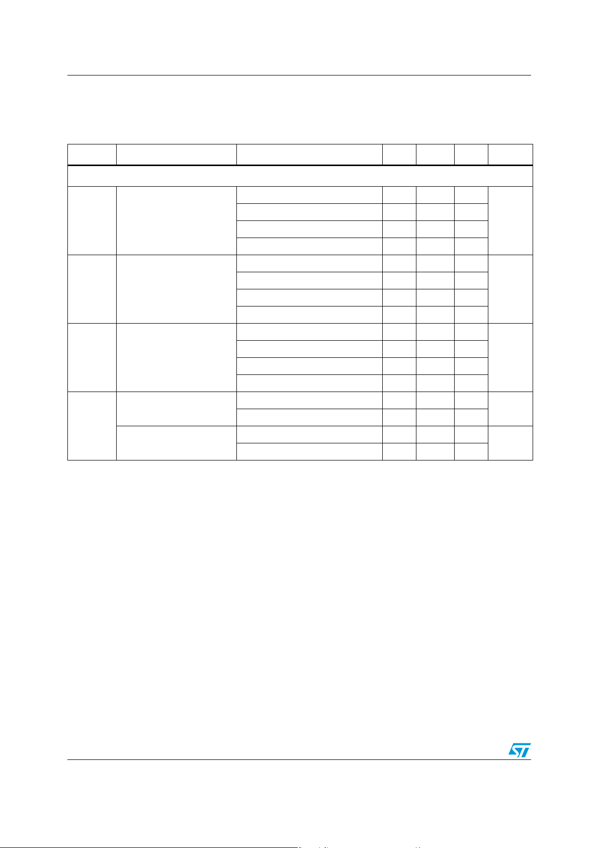
Table 1. Device summary
Without
shut-down
Standard
Vio
Enhanced
Vio
Standard
Single LMV821 LMV821A LMV820 LMV820A
Dual LMV822 LMV822A LMV823 LMV823A
Quad LMV824 LMV824A LMV825 LMV825A
With
shut-down
Vio
Enhanced
Vio
November 2011 Doc ID 022467 Rev 1 1/31
www.st.com
31

Contents LMV82x, LMV82xA
Contents
1 Package pin connections . . . . . . . . . . . . . . . . . . . . . . . . . . . . . . . . . . . . . 3
2 Absolute maximum ratings and operating conditions . . . . . . . . . . . . . 4
3 Electrical characteristics . . . . . . . . . . . . . . . . . . . . . . . . . . . . . . . . . . . . . 6
4 Application information . . . . . . . . . . . . . . . . . . . . . . . . . . . . . . . . . . . . . 16
4.1 Operating voltages . . . . . . . . . . . . . . . . . . . . . . . . . . . . . . . . . . . . . . . . . . 16
4.2 Input common mode range . . . . . . . . . . . . . . . . . . . . . . . . . . . . . . . . . . . 16
4.3 Rail-to-rail output . . . . . . . . . . . . . . . . . . . . . . . . . . . . . . . . . . . . . . . . . . . 16
4.4 Input offset voltage drift over temperature . . . . . . . . . . . . . . . . . . . . . . . . 16
4.5 PCB layouts . . . . . . . . . . . . . . . . . . . . . . . . . . . . . . . . . . . . . . . . . . . . . . . 16
4.6 Macromodel . . . . . . . . . . . . . . . . . . . . . . . . . . . . . . . . . . . . . . . . . . . . . . . 16
4.7 Shutdown function . . . . . . . . . . . . . . . . . . . . . . . . . . . . . . . . . . . . . . . . . . 17
5 Package information . . . . . . . . . . . . . . . . . . . . . . . . . . . . . . . . . . . . . . . . 18
5.1 SO-8 package information . . . . . . . . . . . . . . . . . . . . . . . . . . . . . . . . . . . . 19
5.2 SO-14 package information . . . . . . . . . . . . . . . . . . . . . . . . . . . . . . . . . . . 20
5.3 TSSOP14 package information . . . . . . . . . . . . . . . . . . . . . . . . . . . . . . . . 21
5.4 TSSOP16 package information . . . . . . . . . . . . . . . . . . . . . . . . . . . . . . . . 22
5.5 MiniSO-8 package information . . . . . . . . . . . . . . . . . . . . . . . . . . . . . . . . . 23
5.6 MiniSO-10 package information . . . . . . . . . . . . . . . . . . . . . . . . . . . . . . . . 24
5.7 DFN8 package information . . . . . . . . . . . . . . . . . . . . . . . . . . . . . . . . . . . . 25
5.8 SOT23-5 package information . . . . . . . . . . . . . . . . . . . . . . . . . . . . . . . . . 26
5.9 SOT23-6 package information . . . . . . . . . . . . . . . . . . . . . . . . . . . . . . . . . 27
5.10 SC70-5 (or SOT323-5) package information . . . . . . . . . . . . . . . . . . . . . . 28
6 Ordering information . . . . . . . . . . . . . . . . . . . . . . . . . . . . . . . . . . . . . . . 29
7 Revision history . . . . . . . . . . . . . . . . . . . . . . . . . . . . . . . . . . . . . . . . . . . 30
2/31 Doc ID 022467 Rev 1
LMV82x, LMV82xA Package pin connections
4
5
6
2
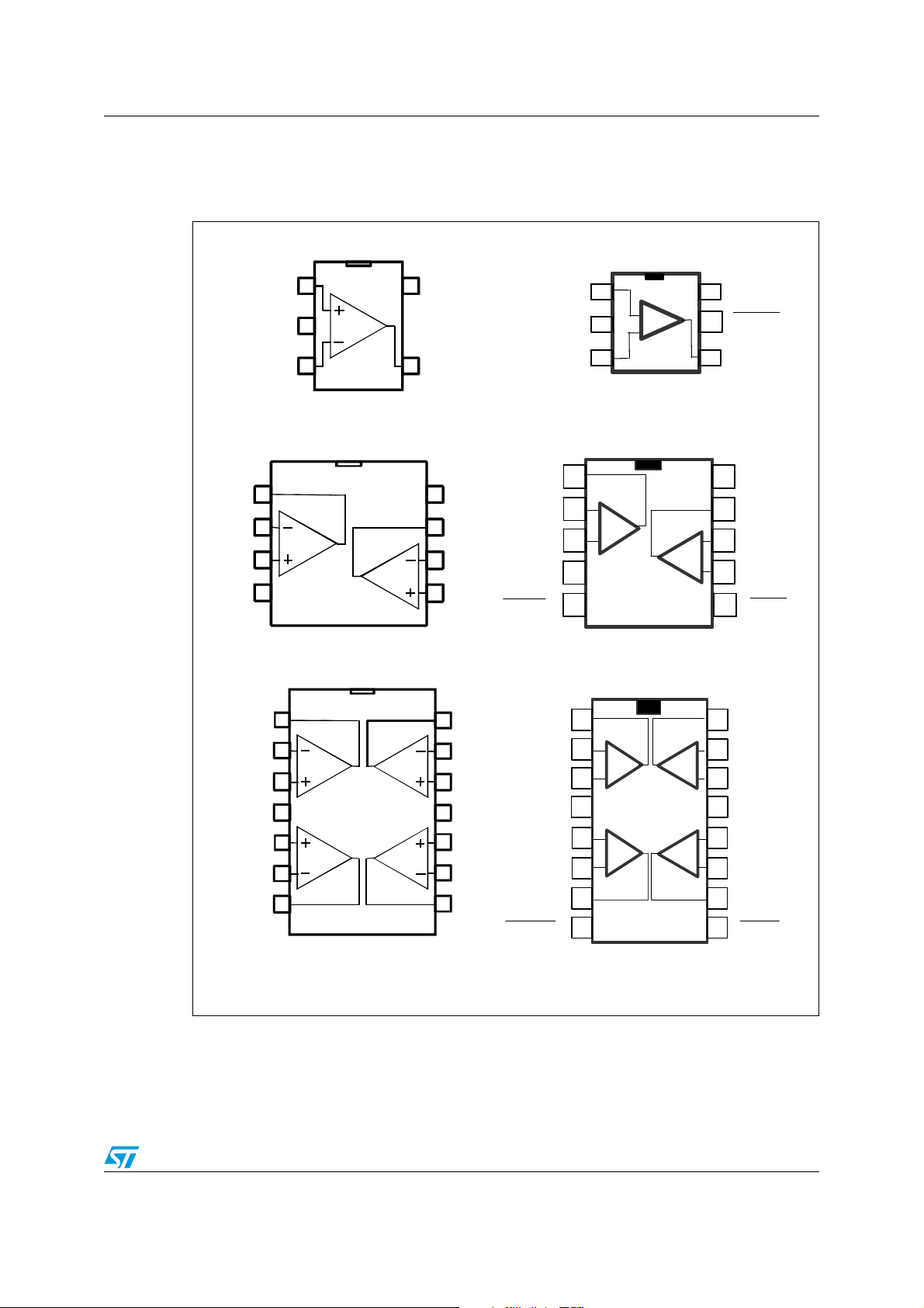
1 Package pin connections
Figure 1. Pin connections for each package (top view)
Out1
In1-
In1+
1
In+
2
Vcc-
In- Out
3
SC70-5 / SOT23-5
1
2
3
4Vcc-
DFN8 / MiniSO8
1
Out1
2
In1-
3
In1+
4Vcc+
In2+
In2-
7
Out
5
Vcc+
4
Vcc+
8
Out2
7
In2-
6
5In2+
14
Out4
13
In
In4+
12
11
Vcc-
10
In3+
In3-
9
8
Out3
SHDN1
SHDN1SHDN1
-
SHDN1/2
SHDN1/2
Out1
Out1
In1-
In1-
In1+
In1+
V
V
CC-
CC-
Out1
In1-
In1+
V
In2+
In2-
Out2
In+
1
1
+
+
_
V
CC-
In-
2
2
3
3
_
SOT23-6
1
1
_
_
2
2
+
+
3
3
4
4
5 6
5 6
MiniSO10
1
_
2
+
3
CC+
5
+
_
6
7 10
8 9
V
6
6
CC+
5
SHDN
4
4
Out
10
10
V
V
CC+
CC+
9
9
Out2
Out2
_
_
+
+
_
+
+
_
16
15
14
134
12
11
8
8
7
7
In2-
In2-
In2+
In2+
SHDN2
SHDN2
SHDN2
Out4
In4-
In4+
V
CC-
In3+
In3-
Out3
SHDN3/4SHDN3/4
TSSOP14 / SO14
TSSOP16
Doc ID 022467 Rev 1 3/31
Absolute maximum ratings and operating conditions LMV82x, LMV82xA
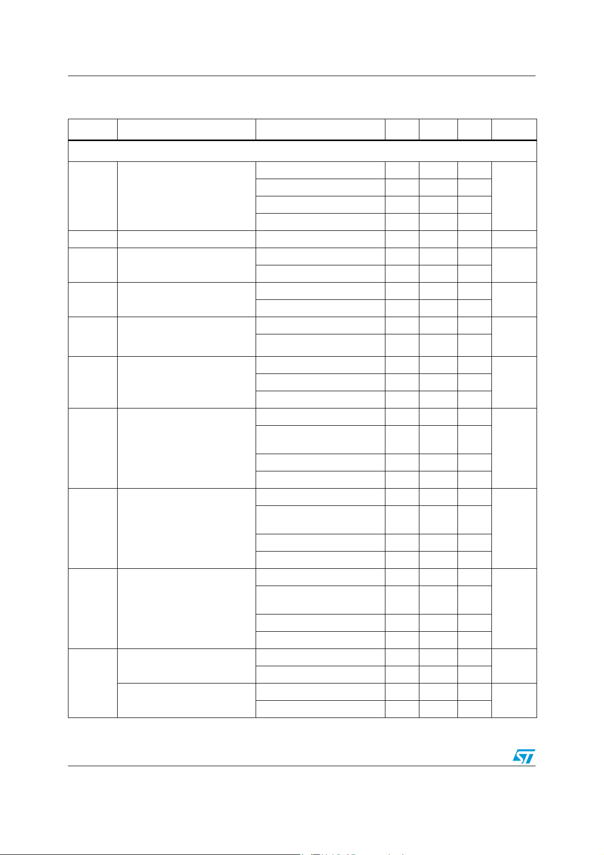
2 Absolute maximum ratings and operating conditions
Table 2. Absolute maximum ratings (AMR)
Symbol Parameter Value Unit
(4)
(1)
(5)
(9)
(2)
(10)
(3)
(10)
(6)(7)
(8)
(8)
6V
±V
cc
V
- 0.3 to V
cc-
+ 0.3 V
cc+
10 mA
V
- 0.2 to V
cc-
+ 0.2 V
cc+
4kV
3.5 kV
250 V
1.3 kV
1kV
V
V
V
I
Supply voltage
cc
Differential input voltage
id
Input pins (IN+ and IN- pins) voltage
in
Input current
in
SHDN Shutdown voltage
T
Storage temperature -65 to +150 °C
stg
Thermal resistance junction to ambient
–SC70-5 205
–SOT23-5 250
– DFN8 2x2 57
– MiniSO8 190
R
thja
–SO8 125
– TSSOP14 100
–SO14 105
–SOT23-6 240
– MiniSO10 113
– TSSOP16 95
T
Maximum junction temperature 150 °C
j
HBM: human body model (except shutdown pin)
HBM: human body model (shutdown pin)
ESD
MM: machine model
CDM: charged device model
CDM: charged device model LMV825
Latch-up immunity 200 mA
1. All voltage values, except the differential voltage are with respect to the network ground terminal.
2. Differential voltages are the non-inverting input terminal with respect to the inverting input terminal.
3. Vcc-Vin must not exceed 6 V, Vin must not exceed 6 V.
4. The input current must be limited by a resistor in series with the inputs.
5. Vcc-V
6. Short-circuits can cause excessive heating and destructive dissipation.
7. R
8. Human body model: a 100 pF capacitor is discharged through a 1.5 kΩ resistor between two pins of the
device. This is done for all couples of pin combinations while other pins are floating.
9. Machine model: a 200 pF capacitor is charged to the specified voltage, then discharged directly between
two pins of the device with no external series resistor (internal resistor < 5 Ω). This is done for all couples of
pin combinations while other pins are floating.
10. Charged device model: all pins and package are charged together to the specified voltage and then
discharged directly to ground.
must not exceed 6 V, Vin must not exceed 6 V.
shdn
are typical values.
th
V
°C/W
4/31 Doc ID 022467 Rev 1
LMV82x, LMV82xA Absolute maximum ratings and operating conditions
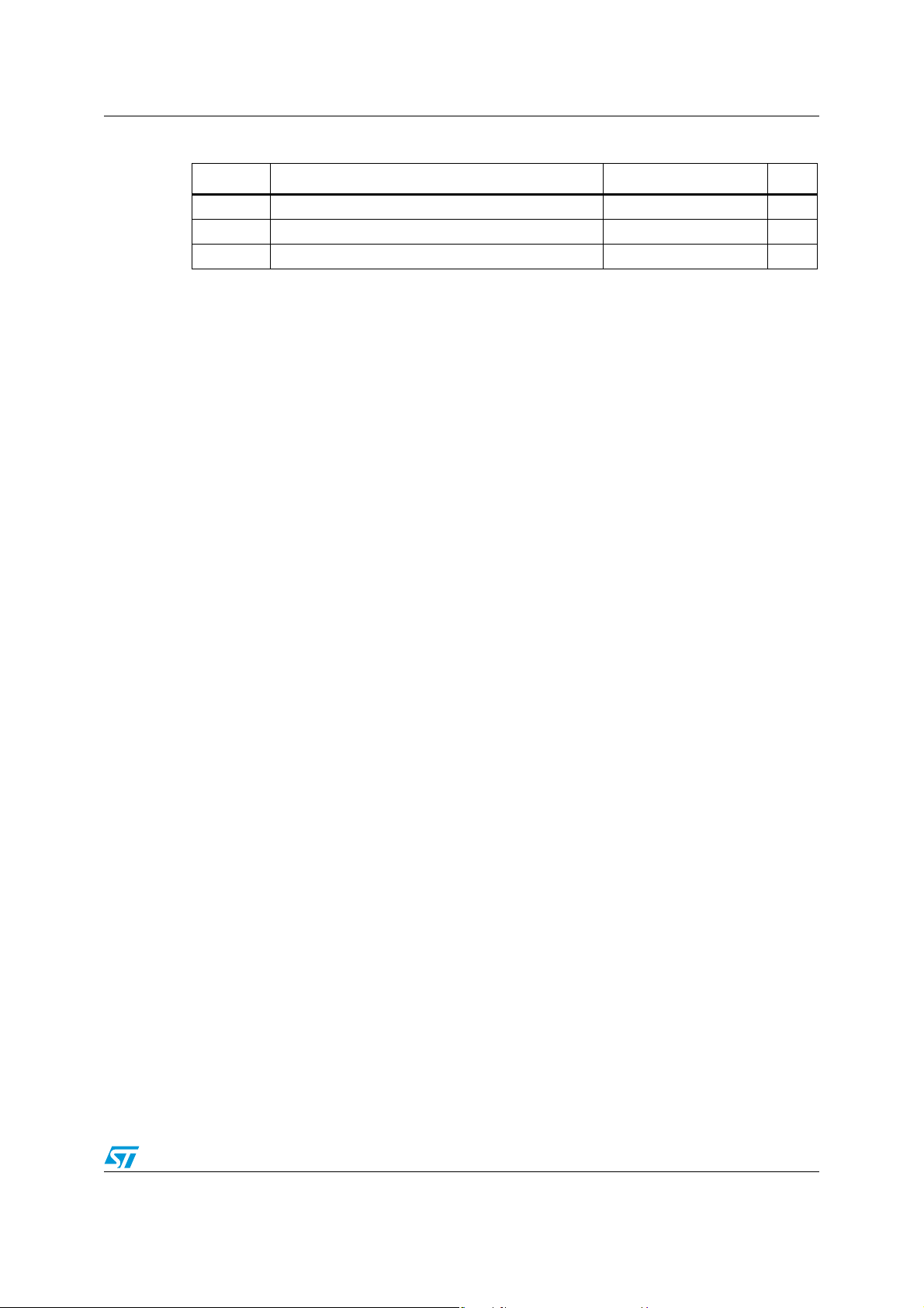
Table 3. Operating conditions
Symbol Parameter Value Unit
T
V
V
oper
cc
icm
Supply voltage 2.5 to 5.5 V
Common mode input voltage range V
- 0.2 to V
cc-
- 1 V
cc+
Operating free air temperature range -40 to +125 °C
Doc ID 022467 Rev 1 5/31
Electrical characteristics LMV82x, LMV82xA
3 Electrical characteristics
Table 4. Electrical characteristics at V
Symbol Parameter Conditions Min. Typ. Max. Unit
DC performance
V
io
V
CC-VOH
V
OL
I
out
R
connected to Vcc/2 (unless otherwise specified)
L
= 2.5 V with V
cc+
LMV82xA, T = 25°C 0.8
LMV82x, T = 25°C 3.5
Input offset voltage
LMV82xA, -40°C < T< 125°C 2
LMV82x, -40°C < T< 125°C 4
=600Ω, T = 25°C 220
R
L
R
=600Ω, -40°C < T< 125°C 320
High level output voltage
Low level output voltage
I
sink (Vout
= V
cc)
Vid = -1 V
(V
I
source
out
= 0 V)
Vid = 1 V
L
=2kΩ, T = 25°C 120
R
L
R
=2kΩ, -40°C < T< 125°C 220
L
=600Ω, T = 25°C 220
R
L
R
=600Ω, -40°C < T< 125°C 320
L
R
=2kΩ, T = 25°C 120
L
=2kΩ, -40°C < T< 125°C 200
R
L
T = 25°C 5
-40°C < T< 125°C 5
T = 25°C 5
-40°C < T< 125°C 5
= 0 V, V
cc-
= Vcc/2, T
icm
= 25° C, and
amb
mV
mV
mV
mA
mA
6/31 Doc ID 022467 Rev 1
LMV82x, LMV82xA Electrical characteristics
Table 5. Shutdown characteristics VCC=2.5V
Symbol Parameter Conditions Min. Typ. Max. Unit
DC performance
T= 25°C 2.5 50 nA
-40°C < T< 85°C 200 nA
-40°C < T< 125°C 1.5 µA
RL=2kΩ,
V
RL=2kΩ, Vout = V
V
SHDN
-40°C < T< 125°C 1 nA
I
CC
t
on
t
off
V
V
I
IH
I
IL
I
OLeak
Supply current in shutdown
mode (all operators)
SHDN = V
Amplifier turn-on time
Amplifier turn-off time
SHDN logic high
IH
SHDN logic low 0.5 V
IL
CC-
(1)
(1)
SHDN current high SHDN =V
SHDN current low SHDN =V
Output leakage in shutdown
mode
1. See Section 4.7: Shutdown function on page 17.
out=VCC-
-1.2V
CC+
=V
to V
CC+
CC-
CC-
CC -
+0.2V
-1V to
CC+
V
0.5
300 ns
20 ns
-
cc
10 pA
10 pA
50 pA
V
Doc ID 022467 Rev 1 7/31
Electrical characteristics LMV82x, LMV82xA
Table 6. Electrical characteristics at V
R
connected to Vcc/2 (unless otherwise specified)
L
= 2.7 V with V
cc+
= 0 V, V
cc-
= Vcc/2, T
icm
Symbol Parameter Conditions Min. Typ. Max. Unit
DC performance
LMV82xA, T = 25°C 0.8
LMV82x, T = 25°C 3.5
V
Input offset voltage
io
LMV82xA, -40°C < T< 125°C 2
LMV82x, -40°C < T< 125°C 4
ΔVio/ΔT Input offset voltage drift
Input offset current
I
io
(V
out=Vcc
/2)
(1)
-40°C < T< 125°C 1 μV/°C
T = 25°C 0.5 30
-40°C < T< 125°C 1 50
T = 25°C 60 120
Input bias current (V
I
ib
Common mode rejection ratio
CMR
A
20 log (ΔV
ic = 0 V to V
V
Large signal voltage gain
vd
= 0.5V to (Vcc-0.5V)
V
out
VCC-VOHHigh level output voltage
V
Low level output voltage
OL
I
sink (Vout
= V
Vid = -1 V
I
out
I
source
(V
out
Vid = 1 V
I
Supply current (per channel)
CC
No load, V
/ΔVio)
icm
cc
cc)
= 0 V)
= Vcc/2
out
-1V, V
out=Vcc
out
= V
/2)
-40°C < T< 125°C 180
T = 25°C 70 75
-40°C < T< 125°C 68
/2
cc
R
= 600 Ω, T = 25°C 90 100
L
R
= 600 Ω, -40°C < T< 125°C 85
L
R
=2kΩ, T = 25°C 95 100
L
=2kΩ, -40°C < T< 125°C 90
R
L
= 600 Ω, T = 25°C 200
R
L
R
= 600 Ω, -40°C < T< 125°C 300
L
=2kΩ, T = 25°C 100
R
L
=2kΩ, -40°C < T< 125°C 200
R
L
= 600 Ω, T = 25°C 200
R
L
R
= 600 Ω, -40°C < T< 125°C 300
L
=2kΩ, T = 25°C 120
R
L
R
=2kΩ, -40°C < T< 125°C 200
L
T = 25°C 15 26
-40°C < T< 125°C 12
T = 25°C 15 21
-40°C < T< 125°C 12
T = 25°C 220 300
-40°C < T< 125°C 500
= 25° C, and
amb
mV
nA
nA
dB
dB
mV
mV
mA
mA
µA
8/31 Doc ID 022467 Rev 1
LMV82x, LMV82xA Electrical characteristics
A
Table 6. Electrical characteristics at V
R
connected to Vcc/2 (unless otherwise specified) (continued)
L
= 2.7 V with V
cc+
= 0 V, V
cc-
= Vcc/2, T
icm
= 25° C, and
amb
Symbol Parameter Conditions Min. Typ. Max. Unit
AC performance
GBP Gain bandwidth product R
F
Unity gain frequency RL>1MΩ, CL=22pF 4.5 MHz
u
Φ
G
Phase margin RL>1MΩ, CL= 22 pF 60 degrees
m
Gain margin RL>1MΩ, CL=22pF 10 dB
m
SR Slew rate
Equivalent input noise voltage
e
n
Equivalent input noise current f = 1 kHz 0.30
i
n
THD+N
Table 7. Shutdown characteristics VCC=2.7V
Total harmonic distortion +
noise
>1MΩ, CL=22pF 5.5 MHz
L
R
>1MΩ, CL=22pF,
L
V
= 0.5 V to VCC-0.5V
out
f=1kHz
f = 10 kHz
= 1 kHz, A
f
in
= 1, RL = 100 kΩ
CL
Vicm = Vcc/2, BW = 22 kHz,
1.2 1.7 V/μs
18
15
0.001 %
Vout = 3 Vpp
nV
-----------Hz
p
-----------Hz
Symbol Parameter Conditions Min. Typ. Max. Unit
DC performance
I
Supply current in shutdown
CC
mode (all operators)
= V
SHDN
CC-
-40°C < T< 85°C 200 nA
2.5 50 nA
-40°C < T< 125°C 1.5 µA
t
t
V
V
I
I
OLeak
1. See Section 4.7: Shutdown function on page 17.
Amplifier turn-on time
on
Amplifier turn-off time
off
SHDN logic high
IH
SHDN logic low 0.5 V
IL
SHDN current high SHDN =V
IH
SHDN current low SHDN =V
I
IL
Output leakage in shutdown
mode
(1)
(1)
RL=2kΩ,
V
out=VCC-
to V
CC -
RL=2kΩ, Vout = V
-1.2V
V
CC+
+0.2V
-1V to
CC+
V
300 ns
20 ns
-
cc
0.5
10 pA
10 pA
50 pA
SHDN
=V
CC+
CC-
CC-
-40°C < T< 125°C 1 nA
V
Doc ID 022467 Rev 1 9/31
Electrical characteristics LMV82x, LMV82xA
Table 8. Electrical characteristics at V
R
connected to Vcc/2 (unless otherwise specified)
L
Symbol Parameter Conditions Min. Typ. Max. Unit
DC performance
V
Input offset voltage
io
ΔVio/ΔT Input offset voltage drift
I
I
Input offset current (V
io
Input bias current (V
ib
out=Vcc
out=Vcc
Common mode rejection ratio 20
CMR
SVR
A
V
CC-VOH
V
I
out
log (ΔV
ic = 0 V to V
V
icm
/ΔVio)
cc
-1V, V
Supply voltage rejection ratio 20
log (ΔV
Large signal voltage gain
vd
V
/ΔVio)
cc
= 0.5V to (Vcc-0.5V)
out
High level output voltage
Low level output voltage
OL
I
sink (Vout
= V
cc)
Vid = -1 V
(V
I
source
V
id
= 1 V
out
= 0 V)
out
(1)
= V
= 5 V with V
cc+
= 0 V, V
cc-
= Vcc/2, T
icm
amb
LMV82xA, T = 25°C 0.8
LMV82x, T = 25°C 3.5
LMV82xA, -40°C < T< 125°C 2
LMV82x, -40°C < T< 125°C 4
-40°C < T< 125°C 1 μV/°C
T = 25°C 0.5 30
/2)
-40°C < T< 125°C 1 50
T = 25°C 60 120
/2)
-40°C < T< 125°C 180
T = 25°C 72 90
-40°C < T< 125°C 70
/
cc
Vcc = 2.5 to 5 V
-40°C < T< 125°C 65
=600Ω, T = 25°C 95 100
R
L
=600Ω, -40°C < T<
R
L
125°C
=2kΩ, T = 25°C 95 100
R
L
=2kΩ, -40°C < T< 125°C 90
R
L
90
RL=600Ω, T = 25°C 250
=600Ω, -40°C < T<
R
L
125°C
R
=2kΩ, T = 25°C 150
L
=2kΩ, -40°C < T< 125°C 200
R
L
R
=600Ω, T = 25°C 250
L
=600Ω, -40°C < T<
R
L
125°C
=2kΩ, T = 25°C 150
R
L
R
=2kΩ, -40°C < T< 125°C 200
L
T = 25°C 35 43
-40°C < T< 125°C 25
T = 25°C 60 70
-40°C < T< 125°C 50
= 25° C, and
mV
nA
nA
dB
dBT = 25°C 70 75
dB
400
mV
300
mV
mA
mA
10/31 Doc ID 022467 Rev 1