

LMV82x, LMV82xA
Low power, high accuracy, general-purpose operational amplifier
Features
■ Low power consumption: 400 µA max at 5 V
■ Low power shutdown mode: 50 nA max
■ Low offset voltage: 0.8 mV max at 25°C
■ Tiny packages
■ Extended temperature range: -40°C to +125°C
■ Low supply voltage: 2.5 V - 5.5 V
■ Gain bandwidth product: 5.5 MHz
Benefits
■ Longer lifetime in battery-powered applications
■ Higher accuracy without calibration
■ Smaller form factor than equivalent competitor
devices
■ Application performances guaranteed over
wide temperature range
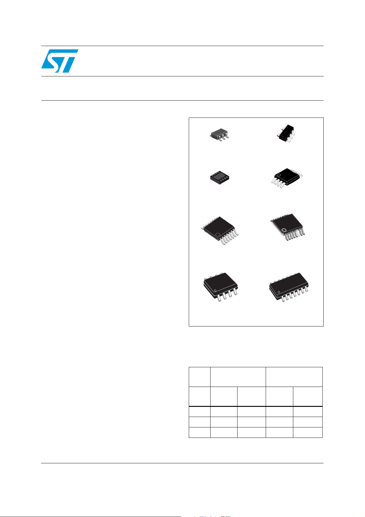
SC70-5
DFN8 2x2
TSSOP14
SOT23-5 / SOT23-6
MiniSO8 / MiniSO10
TSSOP16
Related products
■ See TSV85x series for lower power
consumption (180 µA max at 5 V)
Applications
■ Battery-powered applications
■ Portable devices
■ Signal conditioning
■ Active filtering
■ Medical instrumentation
Description
The LMV82x series of single, dual and quad
operational amplifiers offers low voltage operation
with rail-to-rail output swing. The LMV82x series
outperforms the industry standard LMV321
especially with regard to the gain bandwidth
product (5.5 MHz). The LMV821, LMV822 and
LMV824 are proposed with standard pinouts.
SO8
SO14
The LMV820, LMV823 and LMV825 include a
power-saving shutdown feature that reduces the
supply current to a maximum of 50 nA at 25°C.
Table 1. Device summary
Without
shut-down
Standard
Vio
Enhanced
Vio
Standard
Single LMV821 LMV821A LMV820 LMV820A
Dual LMV822 LMV822A LMV823 LMV823A
Quad LMV824 LMV824A LMV825 LMV825A
With
shut-down
Vio
Enhanced
Vio
November 2011 Doc ID 022467 Rev 1 1/31
www.st.com
31

Contents LMV82x, LMV82xA
Contents
1 Package pin connections . . . . . . . . . . . . . . . . . . . . . . . . . . . . . . . . . . . . . 3
2 Absolute maximum ratings and operating conditions . . . . . . . . . . . . . 4
3 Electrical characteristics . . . . . . . . . . . . . . . . . . . . . . . . . . . . . . . . . . . . . 6
4 Application information . . . . . . . . . . . . . . . . . . . . . . . . . . . . . . . . . . . . . 16
4.1 Operating voltages . . . . . . . . . . . . . . . . . . . . . . . . . . . . . . . . . . . . . . . . . . 16
4.2 Input common mode range . . . . . . . . . . . . . . . . . . . . . . . . . . . . . . . . . . . 16
4.3 Rail-to-rail output . . . . . . . . . . . . . . . . . . . . . . . . . . . . . . . . . . . . . . . . . . . 16
4.4 Input offset voltage drift over temperature . . . . . . . . . . . . . . . . . . . . . . . . 16
4.5 PCB layouts . . . . . . . . . . . . . . . . . . . . . . . . . . . . . . . . . . . . . . . . . . . . . . . 16
4.6 Macromodel . . . . . . . . . . . . . . . . . . . . . . . . . . . . . . . . . . . . . . . . . . . . . . . 16
4.7 Shutdown function . . . . . . . . . . . . . . . . . . . . . . . . . . . . . . . . . . . . . . . . . . 17
5 Package information . . . . . . . . . . . . . . . . . . . . . . . . . . . . . . . . . . . . . . . . 18
5.1 SO-8 package information . . . . . . . . . . . . . . . . . . . . . . . . . . . . . . . . . . . . 19
5.2 SO-14 package information . . . . . . . . . . . . . . . . . . . . . . . . . . . . . . . . . . . 20
5.3 TSSOP14 package information . . . . . . . . . . . . . . . . . . . . . . . . . . . . . . . . 21
5.4 TSSOP16 package information . . . . . . . . . . . . . . . . . . . . . . . . . . . . . . . . 22
5.5 MiniSO-8 package information . . . . . . . . . . . . . . . . . . . . . . . . . . . . . . . . . 23
5.6 MiniSO-10 package information . . . . . . . . . . . . . . . . . . . . . . . . . . . . . . . . 24
5.7 DFN8 package information . . . . . . . . . . . . . . . . . . . . . . . . . . . . . . . . . . . . 25
5.8 SOT23-5 package information . . . . . . . . . . . . . . . . . . . . . . . . . . . . . . . . . 26
5.9 SOT23-6 package information . . . . . . . . . . . . . . . . . . . . . . . . . . . . . . . . . 27
5.10 SC70-5 (or SOT323-5) package information . . . . . . . . . . . . . . . . . . . . . . 28
6 Ordering information . . . . . . . . . . . . . . . . . . . . . . . . . . . . . . . . . . . . . . . 29
7 Revision history . . . . . . . . . . . . . . . . . . . . . . . . . . . . . . . . . . . . . . . . . . . 30
2/31 Doc ID 022467 Rev 1
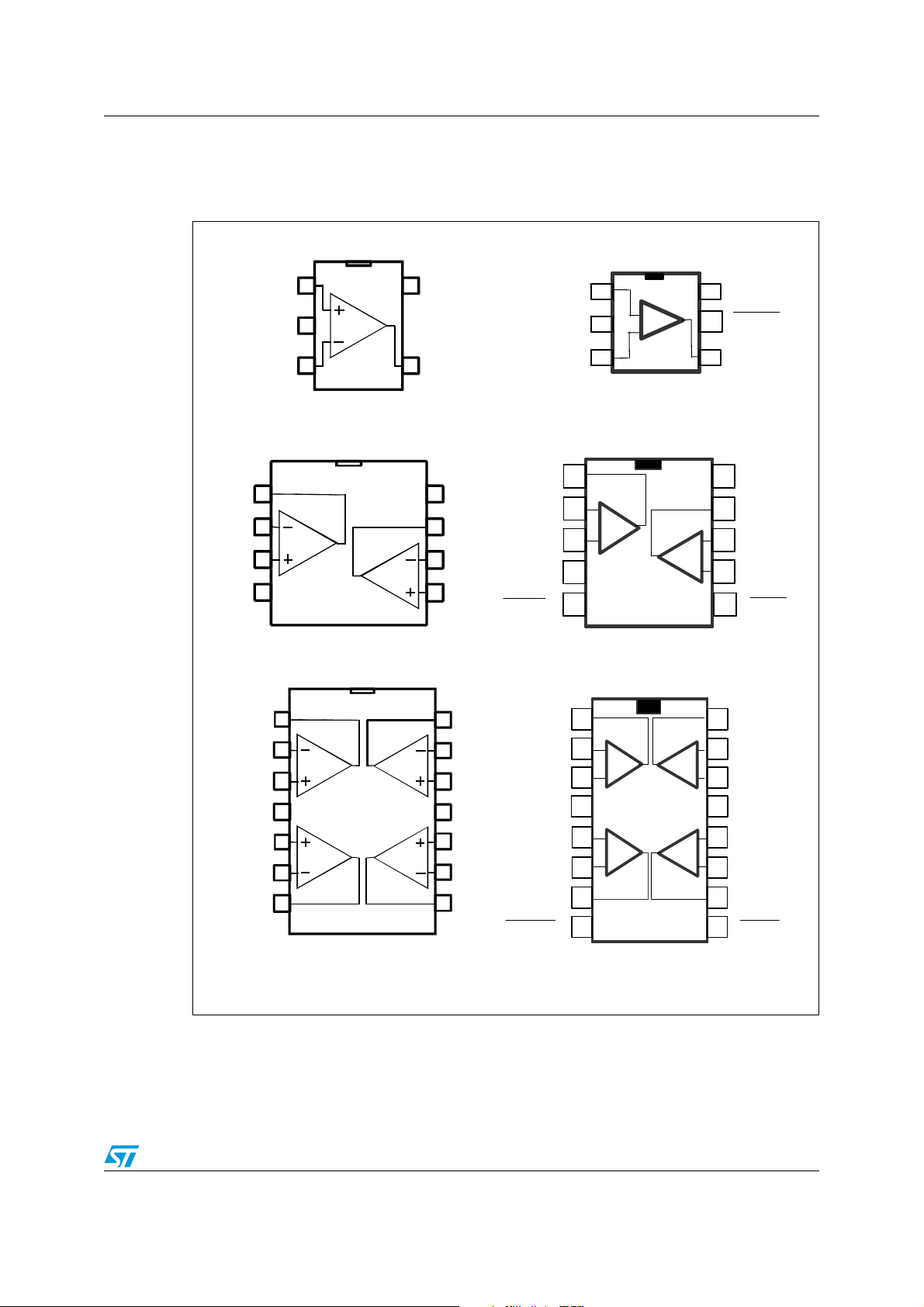
LMV82x, LMV82xA Package pin connections
4
5
6
2
1 Package pin connections
Figure 1. Pin connections for each package (top view)
Out1
In1-
In1+
1
In+
2
Vcc-
In- Out
3
SC70-5 / SOT23-5
1
2
3
4Vcc-
DFN8 / MiniSO8
1
Out1
2
In1-
3
In1+
4Vcc+
In2+
In2-
7
Out
5
Vcc+
4
Vcc+
8
Out2
7
In2-
6
5In2+
14
Out4
13
In
In4+
12
11
Vcc-
10
In3+
In3-
9
8
Out3
SHDN1
SHDN1SHDN1
-
SHDN1/2
SHDN1/2
Out1
Out1
In1-
In1-
In1+
In1+
V
V
CC-
CC-
Out1
In1-
In1+
V
In2+
In2-
Out2
In+
1
1
+
+
_
V
CC-
In-
2
2
3
3
_
SOT23-6
1
1
_
_
2
2
+
+
3
3
4
4
5 6
5 6
MiniSO10
1
_
2
+
3
CC+
5
+
_
6
7 10
8 9
V
6
6
CC+
5
SHDN
4
4
Out
10
10
V
V
CC+
CC+
9
9
Out2
Out2
_
_
+
+
_
+
+
_
16
15
14
134
12
11
8
8
7
7
In2-
In2-
In2+
In2+
SHDN2
SHDN2
SHDN2
Out4
In4-
In4+
V
CC-
In3+
In3-
Out3
SHDN3/4SHDN3/4
TSSOP14 / SO14
TSSOP16
Doc ID 022467 Rev 1 3/31
Absolute maximum ratings and operating conditions LMV82x, LMV82xA
2 Absolute maximum ratings and operating conditions
Table 2. Absolute maximum ratings (AMR)
Symbol Parameter Value Unit
(4)
(1)
(5)
(9)
(2)
(10)
(3)
(10)
(6)(7)
(8)
(8)
6V
±V
cc
V
- 0.3 to V
cc-
+ 0.3 V
cc+
10 mA
V
- 0.2 to V
cc-
+ 0.2 V
cc+
4kV
3.5 kV
250 V
1.3 kV
1kV
V
V
V
I
Supply voltage
cc
Differential input voltage
id
Input pins (IN+ and IN- pins) voltage
in
Input current
in
SHDN Shutdown voltage
T
Storage temperature -65 to +150 °C
stg
Thermal resistance junction to ambient
–SC70-5 205
–SOT23-5 250
– DFN8 2x2 57
– MiniSO8 190
R
thja
–SO8 125
– TSSOP14 100
–SO14 105
–SOT23-6 240
– MiniSO10 113
– TSSOP16 95
T
Maximum junction temperature 150 °C
j
HBM: human body model (except shutdown pin)
HBM: human body model (shutdown pin)
ESD
MM: machine model
CDM: charged device model
CDM: charged device model LMV825
Latch-up immunity 200 mA
1. All voltage values, except the differential voltage are with respect to the network ground terminal.
2. Differential voltages are the non-inverting input terminal with respect to the inverting input terminal.
3. Vcc-Vin must not exceed 6 V, Vin must not exceed 6 V.
4. The input current must be limited by a resistor in series with the inputs.
5. Vcc-V
6. Short-circuits can cause excessive heating and destructive dissipation.
7. R
8. Human body model: a 100 pF capacitor is discharged through a 1.5 kΩ resistor between two pins of the
device. This is done for all couples of pin combinations while other pins are floating.
9. Machine model: a 200 pF capacitor is charged to the specified voltage, then discharged directly between
two pins of the device with no external series resistor (internal resistor < 5 Ω). This is done for all couples of
pin combinations while other pins are floating.
10. Charged device model: all pins and package are charged together to the specified voltage and then
discharged directly to ground.
must not exceed 6 V, Vin must not exceed 6 V.
shdn
are typical values.
th
V
°C/W
4/31 Doc ID 022467 Rev 1
LMV82x, LMV82xA Absolute maximum ratings and operating conditions
Table 3. Operating conditions
Symbol Parameter Value Unit
T
V
V
oper
cc
icm
Supply voltage 2.5 to 5.5 V
Common mode input voltage range V
- 0.2 to V
cc-
- 1 V
cc+
Operating free air temperature range -40 to +125 °C
Doc ID 022467 Rev 1 5/31
Electrical characteristics LMV82x, LMV82xA
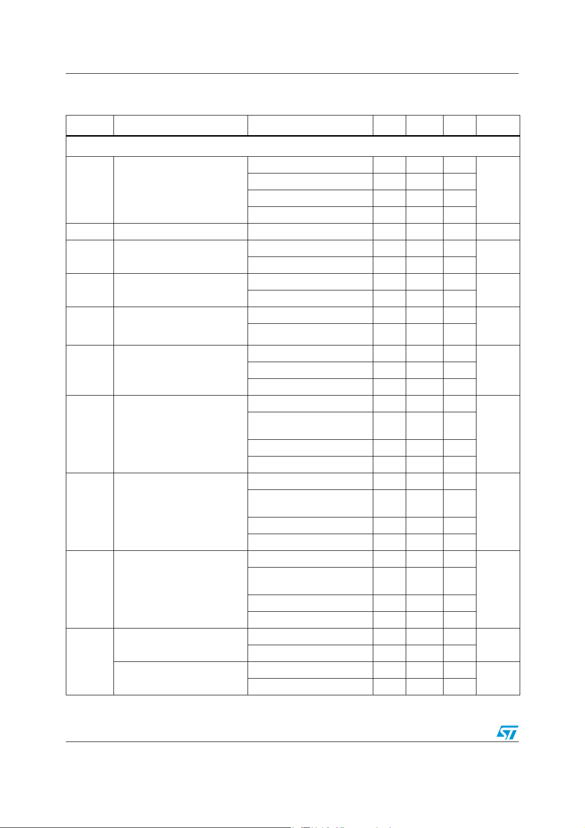
3 Electrical characteristics
Table 4. Electrical characteristics at V
Symbol Parameter Conditions Min. Typ. Max. Unit
DC performance
V
io
V
CC-VOH
V
OL
I
out
R
connected to Vcc/2 (unless otherwise specified)
L
= 2.5 V with V
cc+
LMV82xA, T = 25°C 0.8
LMV82x, T = 25°C 3.5
Input offset voltage
LMV82xA, -40°C < T< 125°C 2
LMV82x, -40°C < T< 125°C 4
=600Ω, T = 25°C 220
R
L
R
=600Ω, -40°C < T< 125°C 320
High level output voltage
Low level output voltage
I
sink (Vout
= V
cc)
Vid = -1 V
(V
I
source
out
= 0 V)
Vid = 1 V
L
=2kΩ, T = 25°C 120
R
L
R
=2kΩ, -40°C < T< 125°C 220
L
=600Ω, T = 25°C 220
R
L
R
=600Ω, -40°C < T< 125°C 320
L
R
=2kΩ, T = 25°C 120
L
=2kΩ, -40°C < T< 125°C 200
R
L
T = 25°C 5
-40°C < T< 125°C 5
T = 25°C 5
-40°C < T< 125°C 5
= 0 V, V
cc-
= Vcc/2, T
icm
= 25° C, and
amb
mV
mV
mV
mA
mA
6/31 Doc ID 022467 Rev 1
LMV82x, LMV82xA Electrical characteristics
Table 5. Shutdown characteristics VCC=2.5V
Symbol Parameter Conditions Min. Typ. Max. Unit
DC performance
T= 25°C 2.5 50 nA
-40°C < T< 85°C 200 nA
-40°C < T< 125°C 1.5 µA
RL=2kΩ,
V
RL=2kΩ, Vout = V
V
SHDN
-40°C < T< 125°C 1 nA
I
CC
t
on
t
off
V
V
I
IH
I
IL
I
OLeak
Supply current in shutdown
mode (all operators)
SHDN = V
Amplifier turn-on time
Amplifier turn-off time
SHDN logic high
IH
SHDN logic low 0.5 V
IL
CC-
(1)
(1)
SHDN current high SHDN =V
SHDN current low SHDN =V
Output leakage in shutdown
mode
1. See Section 4.7: Shutdown function on page 17.
out=VCC-
-1.2V
CC+
=V
to V
CC+
CC-
CC-
CC -
+0.2V
-1V to
CC+
V
0.5
300 ns
20 ns
-
cc
10 pA
10 pA
50 pA
V
Doc ID 022467 Rev 1 7/31
Electrical characteristics LMV82x, LMV82xA
Table 6. Electrical characteristics at V
R
connected to Vcc/2 (unless otherwise specified)
L
= 2.7 V with V
cc+
= 0 V, V
cc-
= Vcc/2, T
icm
Symbol Parameter Conditions Min. Typ. Max. Unit
DC performance
LMV82xA, T = 25°C 0.8
LMV82x, T = 25°C 3.5
V
Input offset voltage
io
LMV82xA, -40°C < T< 125°C 2
LMV82x, -40°C < T< 125°C 4
ΔVio/ΔT Input offset voltage drift
Input offset current
I
io
(V
out=Vcc
/2)
(1)
-40°C < T< 125°C 1 μV/°C
T = 25°C 0.5 30
-40°C < T< 125°C 1 50
T = 25°C 60 120
Input bias current (V
I
ib
Common mode rejection ratio
CMR
A
20 log (ΔV
ic = 0 V to V
V
Large signal voltage gain
vd
= 0.5V to (Vcc-0.5V)
V
out
VCC-VOHHigh level output voltage
V
Low level output voltage
OL
I
sink (Vout
= V
Vid = -1 V
I
out
I
source
(V
out
Vid = 1 V
I
Supply current (per channel)
CC
No load, V
/ΔVio)
icm
cc
cc)
= 0 V)
= Vcc/2
out
-1V, V
out=Vcc
out
= V
/2)
-40°C < T< 125°C 180
T = 25°C 70 75
-40°C < T< 125°C 68
/2
cc
R
= 600 Ω, T = 25°C 90 100
L
R
= 600 Ω, -40°C < T< 125°C 85
L
R
=2kΩ, T = 25°C 95 100
L
=2kΩ, -40°C < T< 125°C 90
R
L
= 600 Ω, T = 25°C 200
R
L
R
= 600 Ω, -40°C < T< 125°C 300
L
=2kΩ, T = 25°C 100
R
L
=2kΩ, -40°C < T< 125°C 200
R
L
= 600 Ω, T = 25°C 200
R
L
R
= 600 Ω, -40°C < T< 125°C 300
L
=2kΩ, T = 25°C 120
R
L
R
=2kΩ, -40°C < T< 125°C 200
L
T = 25°C 15 26
-40°C < T< 125°C 12
T = 25°C 15 21
-40°C < T< 125°C 12
T = 25°C 220 300
-40°C < T< 125°C 500
= 25° C, and
amb
mV
nA
nA
dB
dB
mV
mV
mA
mA
µA
8/31 Doc ID 022467 Rev 1
LMV82x, LMV82xA Electrical characteristics
A
Table 6. Electrical characteristics at V
R
connected to Vcc/2 (unless otherwise specified) (continued)
L
= 2.7 V with V
cc+
= 0 V, V
cc-
= Vcc/2, T
icm
= 25° C, and
amb
Symbol Parameter Conditions Min. Typ. Max. Unit
AC performance
GBP Gain bandwidth product R
F
Unity gain frequency RL>1MΩ, CL=22pF 4.5 MHz
u
Φ
G
Phase margin RL>1MΩ, CL= 22 pF 60 degrees
m
Gain margin RL>1MΩ, CL=22pF 10 dB
m
SR Slew rate
Equivalent input noise voltage
e
n
Equivalent input noise current f = 1 kHz 0.30
i
n
THD+N
Table 7. Shutdown characteristics VCC=2.7V
Total harmonic distortion +
noise
>1MΩ, CL=22pF 5.5 MHz
L
R
>1MΩ, CL=22pF,
L
V
= 0.5 V to VCC-0.5V
out
f=1kHz
f = 10 kHz
= 1 kHz, A
f
in
= 1, RL = 100 kΩ
CL
Vicm = Vcc/2, BW = 22 kHz,
1.2 1.7 V/μs
18
15
0.001 %
Vout = 3 Vpp
nV
-----------Hz
p
-----------Hz
Symbol Parameter Conditions Min. Typ. Max. Unit
DC performance
I
Supply current in shutdown
CC
mode (all operators)
= V
SHDN
CC-
-40°C < T< 85°C 200 nA
2.5 50 nA
-40°C < T< 125°C 1.5 µA
t
t
V
V
I
I
OLeak
1. See Section 4.7: Shutdown function on page 17.
Amplifier turn-on time
on
Amplifier turn-off time
off
SHDN logic high
IH
SHDN logic low 0.5 V
IL
SHDN current high SHDN =V
IH
SHDN current low SHDN =V
I
IL
Output leakage in shutdown
mode
(1)
(1)
RL=2kΩ,
V
out=VCC-
to V
CC -
RL=2kΩ, Vout = V
-1.2V
V
CC+
+0.2V
-1V to
CC+
V
300 ns
20 ns
-
cc
0.5
10 pA
10 pA
50 pA
SHDN
=V
CC+
CC-
CC-
-40°C < T< 125°C 1 nA
V
Doc ID 022467 Rev 1 9/31
Electrical characteristics LMV82x, LMV82xA
Table 8. Electrical characteristics at V
R
connected to Vcc/2 (unless otherwise specified)
L
Symbol Parameter Conditions Min. Typ. Max. Unit
DC performance
V
Input offset voltage
io
ΔVio/ΔT Input offset voltage drift
I
I
Input offset current (V
io
Input bias current (V
ib
out=Vcc
out=Vcc
Common mode rejection ratio 20
CMR
SVR
A
V
CC-VOH
V
I
out
log (ΔV
ic = 0 V to V
V
icm
/ΔVio)
cc
-1V, V
Supply voltage rejection ratio 20
log (ΔV
Large signal voltage gain
vd
V
/ΔVio)
cc
= 0.5V to (Vcc-0.5V)
out
High level output voltage
Low level output voltage
OL
I
sink (Vout
= V
cc)
Vid = -1 V
(V
I
source
V
id
= 1 V
out
= 0 V)
out
(1)
= V
= 5 V with V
cc+
= 0 V, V
cc-
= Vcc/2, T
icm
amb
LMV82xA, T = 25°C 0.8
LMV82x, T = 25°C 3.5
LMV82xA, -40°C < T< 125°C 2
LMV82x, -40°C < T< 125°C 4
-40°C < T< 125°C 1 μV/°C
T = 25°C 0.5 30
/2)
-40°C < T< 125°C 1 50
T = 25°C 60 120
/2)
-40°C < T< 125°C 180
T = 25°C 72 90
-40°C < T< 125°C 70
/
cc
Vcc = 2.5 to 5 V
-40°C < T< 125°C 65
=600Ω, T = 25°C 95 100
R
L
=600Ω, -40°C < T<
R
L
125°C
=2kΩ, T = 25°C 95 100
R
L
=2kΩ, -40°C < T< 125°C 90
R
L
90
RL=600Ω, T = 25°C 250
=600Ω, -40°C < T<
R
L
125°C
R
=2kΩ, T = 25°C 150
L
=2kΩ, -40°C < T< 125°C 200
R
L
R
=600Ω, T = 25°C 250
L
=600Ω, -40°C < T<
R
L
125°C
=2kΩ, T = 25°C 150
R
L
R
=2kΩ, -40°C < T< 125°C 200
L
T = 25°C 35 43
-40°C < T< 125°C 25
T = 25°C 60 70
-40°C < T< 125°C 50
= 25° C, and
mV
nA
nA
dB
dBT = 25°C 70 75
dB
400
mV
300
mV
mA
mA
10/31 Doc ID 022467 Rev 1

LMV82x, LMV82xA Electrical characteristics
A
Table 8. Electrical characteristics at V
R
connected to Vcc/2 (unless otherwise specified) (continued)
L
= 5 V with V
cc+
= 0 V, V
cc-
= Vcc/2, T
icm
= 25° C, and
amb
Symbol Parameter Conditions Min. Typ. Max. Unit
I
CC
Supply current (per channel)
No load, V
out
= Vcc/2
T = 25°C 300 400
-40°C < T< 125°C 600
AC performance
GBP Gain bandwidth product R
F
Φ
G
Unity gain frequency RL>1MΩ, CL=22pF 4.5 MHz
u
Phase margin RL>1MΩ, CL= 22 pF 60 degrees
m
Gain margin RL=1MΩ, CL=22pF 10 dB
m
SR Slew rate
e
i
Equivalent input noise voltage
n
Equivalent input noise current f = 1 kHz 0.30
n
THD+N Total harmonic distortion + noise
>1MΩ, CL=22pF 5.5 MHz
L
>1MΩ, CL=22pF,
R
L
= 0.5 V to VCC-0.5V
V
out
f=1kHz
f=10kHz
= 1 kHz, A
f
in
CL
= 1,
RL = 100 kΩ,
Vicm = Vcc/2, BW = 22 kHz,
1.4 1.9 V/μs
16
13
0.001 %
Vout = 3 Vpp
µA
nV
-----------Hz
p
-----------Hz
1. See Section 4.4: Input offset voltage drift over temperature.
Table 9. Shutdown characteristics VCC=5V
Symbol Parameter Conditions Min. Typ. Max. Unit
DC performance
Supply current in shutdown
I
t
t
V
V
I
I
OLeak
mode (all operators)
CC
SHDN
= V
CC-
Amplifier turn-on time
on
Amplifier turn-off time
off
SHDN logic high
IH
SHDN logic low 0.5 V
IL
SHDN current high SHDN =V
IH
I
SHDN current low SHDN =V
IL
(1)
(1)
Output leakage in shutdown
mode
T= 25°C 2.5 50 nA
-40°C < T< 85°C 200 nA
-40°C < T< 125°C 1.5 µA
RL=2kΩ,
V
out=VCC-
to V
CC -
RL=2kΩ, Vout = V
-1.2V
V
CC+
+0.2V
-1V to
CC+
V
300 ns
20 ns
-
cc
0.5
10 pA
10 pA
50 pA
SHDN
=V
CC+
CC-
CC-
-40°C < T< 125°C 1 nA
V
1. See Section 4.7: Shutdown function on page 17.
Doc ID 022467 Rev 1 11/31

Electrical characteristics LMV82x, LMV82xA
Figure 2. Supply current vs. supply voltage
at Vicm = V
CC
/2
0.35
0.30
0.25
0.20
0.15
0.10
Supply Current (mA)
T=-40°C
0.05
0.00
2.5 3.0 3.5 4.0 4.5 5.0 5.5
T=125°C
Vicm=2.5V
T=25°C
Supply Voltage (V)
Figure 3. Supply current vs. input common
mode voltage in a follower
configuration at V
1.2
1.0
0.8
0.6
0.4
Supply Current (mA)
0.2
0.0
T=25°C
T=125°C
Vcc=5V
Follower configuration
0.0 0.5 1.0 1.5 2.0 2.5 3.0 3.5 4.0
Input Common Mode Voltage (V)
CC
T=-40°C
= 5 V
Figure 4. Vio distribution at VCC =5 V Figure 5. Input offset voltage vs. input
30
25
20
Vcc=5V
Vicm=2.5V
T=25°C
common mode voltage at V
0.30
0.25
0.20
T=25°C
T=-40°C
CC
= 5 V
15
10
Population ( %)
5
Input Offset Voltage ( mV)
0.15
0.10
0.05
T=125°C
Vcc=5V
0
-3.5 -3.0 -2.5 -2.0 -1.5 -1.0 -0.5 0.0 0.5 1.0 1.5 2.0 2.5 3.0 3.5
Input offset voltage ( mV)
0.00
0.0 0.5 1.0 1.5 2.0 2.5 3.0 3.5 4.0
Input Common Mode Voltage (V)
12/31 Doc ID 022467 Rev 1

LMV82x, LMV82xA Electrical characteristics
Figure 6. Output current vs. output voltage at
V
= 2.7 V
CC
30
Sink
Vid=-1V
2020
10
T=125°C
00
T=125°C
-10
Output Current (mA)
T=25°C
T=25°C
Vcc=2.7V
T=-40°C
T=-40°C
-20-20
Source
-30
0.00.0 0.5 1.01.0 1.5 2.02.0 2.5
Output Voltage (V)
Vid=1V
Figure 8. Output current vs. supply voltage at
Vicm = V
9090
Sink
Vid=-1V
6060
T=125°C
3030
00
-30-30
T=125°C
Output Current (mA)
-60-60
Source
Vid=1V
-90-90
2.02.0 2.5 3.03.0 3.5 4.04.0 4.5 5.05.0 5.5
/2
CC
T=25°C
T=25°C
T=-40°C
Supply Voltage (V)
T=-40°C
Vicm=Vcc/2
Figure 7. Output current vs. output voltage at
VCC = 5 V
75
5050
Sink
Vid=-1V
T=25°C
T=-40°C
25
T=125°C
T=125°C
T=25°C
00
-25
Output Current (mA)
Vcc=5V
T=-40°C
-50-50
Source
-75
0.00.0 0.5 1.01.0 1.5 2.02.0 2.5 3.03.0 3.5 4.04.0 4.5 5.05.0
Output Voltage (V)
Vid=1V
Figure 9. Voltage gain and phase with
CL = 40 pF
Phase
0
-45
-90
-135
-180
-225
-270
Phase (°)
40
30
20
T=-40°C
10
Gain (dB)
0
Vcc=5V
Vicm=2.5V
Rl=10k
-10
Cl=40pF
Gain=-100
-20
10k 100k 1M 10M
Gain
T=25°C
Ω
T=125°C
Frequency (Hz)
Figure 10. Voltage gain and phase with
C
= 100 pF
L
40
30
20
T=-40°C
10
Gain (dB)
0
Vcc=5V
Vicm=2.5V
Rl=10k
-10
-20
Ω
Cl=100pF
Gain=-100
10k 100k 1M 10M
Gain
T=125°C
Frequency (Hz)
T=25°C
Figure 11. Voltage gain and phase with
CL = 200 pF
0
-45
-90
Phase
-135
Phase (°)
-180
-225
-270
Doc ID 022467 Rev 1 13/31
40
30
20
Gain
T=25°C
T=-40°C
10
Gain (dB)
0
Vcc=5V
Vicm=2.5V
Rl=10k
-10
-20
Ω
Cl=200pF
Gain=-100
10k 100k 1M 10M
T=125°C
Frequency (Hz)
Phase
0
-45
-90
-135
-180
-225
-270
Phase (°)

Electrical characteristics LMV82x, LMV82xA
Figure 12. Phase margin vs. output current at
V
= 5 V
CC
80
70
Sink
Source
60
50
40
30
Vcc=5V
Phase Margin (°)
Vicm=2.5V
20
Vload=2.5V
10
Rl=10K
Ω
T=25°C
0
-1.0 -0.8 -0.6 -0.4 -0.2 0.0 0.2 0.4 0.6 0.8 1.0
Cl=40pF
Cl=100pF
Output Current (mA)
Figure 14. Positive and negative slew rate vs.
supply voltage
2.52.5
2.02.0
1.51.5
1.01.0
T=125°C
0.50.5
0.00.0
-0.5-0.5
T=125°C
Slew rate (V/µs)
-1.0-1.0
-1.5-1.5
-2.0-2.0
-2.5-2.5
3.03.0 3. 5 4.04.0 4.5 5.05.0 5.5
T=25°C
T=25°C
Supply Voltage (V)
T=-40°C
Cl=100pF
Rl=1M
Vicm=Vcc/2
Vload=Vcc/2
T=-40°C
Ω
Figure 13. Closed-loop gain in voltage
follower configuration for different
capacitive loads
15
Vcc=5V
Vicm=2.5V
1010
Rl=10k
Ω
T=25°C
5
00
Gain (dB)
-5
-10-10
-15
100k 1M 10M
Cl=200pF
Cl=100pF
Cl=50pF
Cl=20pF
Frequency (Hz)
Figure 15. Positive slew rate at VCC = 5 V with
C
= 100 pF
L
2.02.0
1.5
1.01.0
0.5
0.00.0
-0.5
Output Voltage (V)
-1.0-1.0
T=-40°C
-1.5
-2.0-2.0
01234
Time (µs)
T=125°C
T=25°C
Vcc=5V
Vicm=Vcc/2
Cl=100pF
Rl=1M
Ω
14/31 Doc ID 022467 Rev 1

LMV82x, LMV82xA Electrical characteristics
Figure 16. Negative slew rate at VCC = 5 V with
C
= 100 pF
L
2.02.0
1.51.5
T=125°C
1.01.0
0.50.5
0.00.0
-0.5-0.5
Output Voltage (V)
-1.0-1.0
-1.5-1.5
-2.0-2.0
0.0 0.5 1.0 1. 5
Time (µs)
T=25°C
Vcc=5V
Vicm=Vcc/2
Cl=100pF
Ω
Rl=1M
T=-40°C
Figure 17. Noise vs. frequency at V
100
8080
Vicm=0.5V
60
4040
20
00
Equivalent input noise voltage density (nV/VHz)
100 1000 10000
Vicm=2.5V
Frequency (Hz)
CC
Vcc=5V
T=25°C
= 5 V
Figure 18. 0.1 Hz to 10 Hz noise at VCC = 5 V Figure 19. Distortion + noise vs. frequency
6
Vcc=5V
Vicm=2.5V
4
T=25°C
2
0
-2
10
Vcc=5V
Vicm=(Vcc-1)/2
Vin=3Vpp
Gain=1
BW=80kHz
T=25°C
-3
10
Rl=10k
Ω
-2
Voltage noise (µV)
-4
-6
0246810
Time (s)
Figure 20. Distortion + noise vs. output
voltage
0
10
Rl=100k
-1
10
-2
10
THD + N (%)
Vcc=5V
-3
10
Gain=1
BW=22kHz
Vicm=Vcc/2
T=25°C
-4
10
0.01 0.1 1 10
Ω
Output Voltage (Vpp)
Rl=10k
THD + N (%)
Rl=100k
Ω
-4
10
Ω
100 1000 10000
Frequency (Hz)
Doc ID 022467 Rev 1 15/31

Application information LMV82x, LMV82xA
4 Application information
4.1 Operating voltages
The LMV82x can operate from 2.5 to 5.5 V. The devices’ parameters are fully specified for
2.5, 2.7 and 5 V power supplies. Additionally, the main specifications are guaranteed at
extended temperature ranges from -40° C to +125° C.
4.2 Input common mode range
The LMV82x devices have an input common mode range that includes ground. The input
common mode range is extended from V
reversal.
4.3 Rail-to-rail output
The operational amplifiers’ output levels can go close to the rails: 150 mV maximum above
and below the rail when connected to a 2 kΩ resistive load to
- 0.2 V to V
cc-
- 1 V, with no output phase
cc+
V
/2.
cc
4.4 Input offset voltage drift over temperature
The maximum input voltage drift over temperature variation is defined as follows:
for T
min < T < Tmax.
ΔVio
------------- max
=
ΔT
Vio T() Vio 25° C()–
-----------------------------------------------------
T25° C–
4.5 PCB layouts
For correct operation, it is advised to add 10 nF decoupling capacitors as close as possible
to the power supply pins.
4.6 Macromodel
Accurate macromodels of the LMV82x are available on STMicroelectronics’ web site at
www.st.com. This model is a trade-off between accuracy and complexity (that is, time
simulation) of the LMV82x operational amplifiers. It emulates the nominal performances of a
typical device within the specified operating conditions mentioned in the datasheet. It also
helps to validate a design approach and to select the right operational amplifier, but it does
not replace on-board measurements.
16/31 Doc ID 022467 Rev 1

LMV82x, LMV82xA Application information
4.7 Shutdown function
The operational amplifier is enabled when the SHDN pin is pulled high. To disable the
amplifier, the SHDN
output is in a high impedance state. The SHDN
V
or V
CC+
CC-
The turn-on and turn-off times are calculated for an output variation of ±200 mV (Figure 21
and Figure 22 show the test configurations).
Figure 21. Test configuration for turn-on time
(Vout pulled down)
pin must be pulled down to V
.
. When in shutdown mode, the amplifier
CC-
pin must never be left floating but tied to
Figure 22. Test configuration for turn-off time
(Vout pulled down)
Vcc
Vcc –1V
+
‐
GND
Figure 23. Turn-on time, VCC = 5 V,
Vout pulled down, T = 25° C
3
2
1
0
Voltage (V)
-1
-2
-3
-0.1 0.0 0.1 0.2 0.3 0.4 0.5
Time(µs)
Shutdown pulse
Vout
Vcc = 5V
T = 25°C
RL connected to GND
GND
GND
Vcc
2kΩ
Vcc –1V
+
2kΩ
‐
GND
Figure 24. Turn-off time, VCC = 5 V,
Vout pulled down, T = 25° C
3
2
1
0
-1
Output voltage (V)
-2
-3
-0.05 0.00 0.05 0.10 0.15 0.20
Vcc = 5V
T = 25°C
RL connected to GND
Vout
Shutdown pulse
Time(µs)
Doc ID 022467 Rev 1 17/31

Package information LMV82x, LMV82xA
5 Package information
In order to meet environmental requirements, ST offers these devices in different grades of
ECOPACK
specifications, grade definitions and product status are available at: www.st.com.
ECOPACK
®
packages, depending on their level of environmental compliance. ECOPACK®
®
is an ST trademark.
18/31 Doc ID 022467 Rev 1

LMV82x, LMV82xA Package information
5.1 SO-8 package information
Figure 25. SO-8 package mechanical drawing
Table 10. SO-8 package mechanical data
Dimensions
Ref.
Min. Typ. Max. Min. Typ. Max.
A1.750.069
A1 0.10 0.25 0.004 0.010
A2 1.25 0.049
b 0.28 0.48 0.011 0.019
c 0.17 0.23 0.007 0.010
D 4.80 4.90 5.00 0.189 0.193 0.197
E 5.80 6.00 6.20 0.228 0.236 0.244
E1 3.80 3.90 4.00 0.150 0.154 0.157
e 1.27 0.050
h 0.25 0.50 0.010 0.020
L 0.40 1.27 0.016 0.050
L1 1.04 0.040
k1° 8°1° 8°
ccc 0.10 0.004
Millimeters Inches
Doc ID 022467 Rev 1 19/31

Package information LMV82x, LMV82xA
5.2 SO-14 package information
Figure 26. SO-14 package mechanical drawing
Table 11. SO-14 package mechanical data
Dimensions
Millimeters Inches
Ref.
Min. Typ. Max. Min. Typ. Max.
A 1.35 1.75 0.05 0.068
A1 0.10 0.25 0.004 0.009
A2 1.10 1.65 0.04 0.06
B 0.33 0.51 0.01 0.02
C 0.19 0.25 0.007 0.009
D 8.55 8.75 0.33 0.34
E 3.80 4.0 0.15 0.15
e1.27 0.05
H 5.80 6.20 0.22 0.24
h 0.25 0.50 0.009 0.02
L 0.40 1.27 0.015 0.05
k 8° (max.)
ddd 0.10 0.004
20/31 Doc ID 022467 Rev 1

LMV82x, LMV82xA Package information
5.3 TSSOP14 package information
Figure 27. TSSOP14 package mechanical drawing
Table 12. TSSOP14 package mechanical data
Dimensions
Ref.
Min. Typ. Max. Min. Typ. Max.
A1.200.047
A1 0.05 0.15 0.002 0.004 0.006
A2 0.80 1.00 1.05 0.031 0.039 0.041
b 0.19 0.30 0.007 0.012
c 0.09 0.20 0.004 0.0089
D 4.90 5.00 5.10 0.193 0.197 0.201
E 6.20 6.40 6.60 0.244 0.252 0.260
E1 4.30 4.40 4.50 0.169 0.173 0.176
e 0.65 0.0256
L 0.45 0.60 0.75 0.018 0.024 0.030
L1 1.00 0.039
k0° 8°0° 8°
aaa 0.10 0.004
Millimeters Inches
Doc ID 022467 Rev 1 21/31

Package information LMV82x, LMV82xA
5.4 TSSOP16 package information
Figure 28. TSSOP16 package mechanical drawing
b
Table 13. TSSOP16 package mechanical data
Dimensions
Ref.
Millimeters Inches
Min. Typ. Max. Min. Typ. Max.
A1.200.047
A1 0.05 0.15 0.002 0.006
A2 0.80 1.00 1.05 0.031 0.039 0.041
b 0.19 0.30 0.007 0.012
c 0.09 0.20 0.004 0.008
D 4.90 5.00 5.10 0.193 0.197 0.201
E 6.20 6.40 6.60 0.244 0.252 0.260
E1 4.30 4.40 4.50 0.169 0.173 0.177
e 0.65 0.0256
k0° 8°0° 8°
L 0.45 0.60 0.75 0.018 0.024 0.030
L1 1.00 0.039
aaa 0.10 0.004
22/31 Doc ID 022467 Rev 1

LMV82x, LMV82xA Package information
5.5 MiniSO-8 package information
Figure 29. MiniSO-8 package mechanical drawing
Table 14. MiniSO-8 package mechanical data
Dimensions
Ref.
Millimeters Inches
Min. Typ. Max. Min. Typ. Max.
A 1.1 0.043
A1 0 0.15 0 0.006
A2 0.75 0.85 0.95 0.030 0.033 0.037
b 0.22 0.40 0.009 0.016
c 0.08 0.23 0.003 0.009
D 2.80 3.00 3.20 0.11 0.118 0.126
E 4.65 4.90 5.15 0.183 0.193 0.203
E1 2.80 3.00 3.10 0.11 0.118 0.122
e 0.65 0.026
L 0.40 0.60 0.80 0.016 0.024 0.031
L1 0.95 0.037
L2 0.25 0.010
k0° 8°0° 8°
ccc 0.10 0.004
Doc ID 022467 Rev 1 23/31

Package information LMV82x, LMV82xA
5.6 MiniSO-10 package information
Figure 30. MiniSO-10 package mechanical drawing
Table 15. MiniSO-10 package mechanical data
Dimensions
Ref.
Millimeters Inches
Min. Typ. Max. Min. Typ. Max.
A1.100.043
A1 0.05 0.10 0.15 0.002 0.004 0.006
A2 0.78 0.86 0.94 0.031 0.034 0.037
b 0.25 0.33 0.40 0.010 0.013 0.016
c 0.15 0.23 0.30 0.006 0.009 0.012
D 2.90 3.00 3.10 0.114 0.118 0.122
E 4.75 4.90 5.05 0.187 0.193 0.199
E1 2.90 3.00 3.10 0.114 0.118 0.122
e 0.50 0.020
L 0.40 0.55 0.70 0.016 0.022 0.028
L1 0.95 0.037
k 0°3°6°0°3°6°
aaa 0.10 0.004
24/31 Doc ID 022467 Rev 1

LMV82x, LMV82xA Package information
5.7 DFN8 package information
Figure 31. DFN8 2 x 2 mm package mechanical drawing (pitch 0.5 mm)
Table 16. DFN8 2 x 2 mm package mechanical data (pitch 0.5 mm)
Dimensions
Ref.
Millimeters Inches
Min. Typ. Max. Min. Typ. Max.
A 0.51 0.55 0.60 0.020 0.022 0.024
A1 0.05 0.002
A3 0.15 0.006
b 0.18 0.25 0.30 0.007 0.010 0.012
D 1.85 2.00 2.15 0.073 0.079 0.085
D2 1.45 1.60 1.70 0.057 0.063 0.067
E 1.85 2.00 2.15 0.073 0.079 0.085
E2 0.75 0.90 1.00 0.030 0.035 0.040
e 0.50 0.020
L0.500.020
ddd 0.08 0.003
Doc ID 022467 Rev 1 25/31

Package information LMV82x, LMV82xA
5.8 SOT23-5 package information
Figure 32. SOT23-5L package mechanical drawing
Table 17. SOT23-5L package mechanical data
Dimensions
Ref.
Millimeters Inches
Min. Typ. Max. Min. Typ. Max.
A 0.90 1.20 1.45 0.035 0.047 0.057
A1 0.15 0.006
A2 0.90 1.05 1.30 0.035 0.041 0.051
B 0.35 0.40 0.50 0.013 0.015 0.019
C 0.09 0.15 0.20 0.003 0.006 0.008
D 2.80 2.90 3.00 0.110 0.114 0.118
D1 1.90 0.075
e 0.95 0.037
E 2.60 2.80 3.00 0.102 0.110 0.118
F 1.50 1.60 1.75 0.059 0.063 0.069
L 0.10 0.35 0.60 0.004 0.013 0.023
K 0 degrees 10 degrees
26/31 Doc ID 022467 Rev 1

LMV82x, LMV82xA Package information
5.9 SOT23-6 package information
Figure 33. SOT23-6L package mechanical drawing
Table 18. SOT23-6L package mechanical data
Dimensions
Ref.
Min. Typ. Max. Min. Typ. Max.
A 0.90 1.45 0.035 0.057
A1 0.10 0.004
A2 0.90 1.30 0.035 0.051
b 0.35 0.50 0.013 0.019
c 0.09 0.20 0.003 0.008
D 2.80 3.05 0.110 0.120
E 1.50 1.75 0.060 0.069
e 0.95 0.037
H 2.60 3.00 0.102 0.118
L 0.10 0.60 0.004 0.024
° 0 10°
Millimeters Inches
Doc ID 022467 Rev 1 27/31

Package information LMV82x, LMV82xA
5.10 SC70-5 (or SOT323-5) package information
Figure 34. SC70-5 (or SOT323-5) package mechanical drawing
DIMENSIONS IN MM
GAUGE PLANE
SEATING PLANE
SIDE VIEW
COPLANAR LEADS
TOP VIEW
Table 19. SC70-5 (or SOT323-5) package mechanical data
Dimensions
Ref
Min Typ Max Min Typ Max
A 0.80 1.10 0.032 0.043
A1 0.10 0.004
A2 0.80 0.90 1.00 0.032 0.035 0.039
b 0.15 0.30 0.006 0.012
c 0.10 0.22 0.004 0.009
D 1.80 2.00 2.20 0.071 0.079 0.087
E 1.80 2.10 2.40 0.071 0.083 0.094
E1 1.15 1.25 1.35 0.045 0.049 0.053
e 0.65 0.025
e1 1.30 0.051
L 0.26 0.36 0.46 0.010 0.014 0.018
<0° 8°
Millimeters Inches
28/31 Doc ID 022467 Rev 1

LMV82x, LMV82xA Ordering information
6 Ordering information
Table 20. Order codes
Order code
LMV821ICT
Temperature
range
Package Packing Marking
SC70-5
K1S
LMV821ILT SOT23-5 K155
LMV822IQ2T DFN8 2x2 K1S
LMV822IST MiniSO8 K155
-40° C to +125° C
Tape & reel
LMV822IDT SO8 LMV822I
LMV824IPT TSSOP14 LMV824I
LMV824IDT SO14 LMV824I
LMV821AICT
SC70-5
K1T
LMV821AILT SOT23-5 K156
LMV822AIST MiniSO8 K156
-40° C to +125° C
Tape & reel
LMV822AIDT SO8 LMV822AI
LMV824AIPT TSSOP14 LMV824AI
LMV824AIDT SO14 LMV824AI
Table 21. Order codes (with shut-down pin)
Order code
Temperature
range
Package Packing Marking
LMV820ILT
LMV823IST MiniSO10 K155
-40° C to +125° C
SOT23-6
K155
Tape & reel
LMV825IPT TSSOP16 LMV825I
LMV820AILT
LMV823AIST MiniSO10 K156
-40° C to +125° C
SOT23-6
K156
Tape & reel
LMV825AIPT TSSOP16 LMV825AI
Doc ID 022467 Rev 1 29/31

Revision history LMV82x, LMV82xA
7 Revision history
Table 22. Document revision history
Date Revision Changes
10-Nov-2011 1 Initial release.
30/31 Doc ID 022467 Rev 1

LMV82x, LMV82xA
Please Read Carefully:
Information in this document is provided solely in connection with ST products. STMicroelectronics NV and its subsidiaries (“ST”) reserve the
right to make changes, corrections, modifications or improvements, to this document, and the products and services described herein at any
time, without notice.
All ST products are sold pursuant to ST’s terms and conditions of sale.
Purchasers are solely responsible for the choice, selection and use of the ST products and services described herein, and ST assumes no
liability whatsoever relating to the choice, selection or use of the ST products and services described herein.
No license, express or implied, by estoppel or otherwise, to any intellectual property rights is granted under this document. If any part of this
document refers to any third party products or services it shall not be deemed a license grant by ST for the use of such third party products
or services, or any intellectual property contained therein or considered as a warranty covering the use in any manner whatsoever of such
third party products or services or any intellectual property contained therein.
UNLESS OTHERWISE SET FORTH IN ST’S TERMS AND CONDITIONS OF SALE ST DISCLAIMS ANY EXPRESS OR IMPLIED
WARRANTY WITH RESPECT TO THE USE AND/OR SALE OF ST PRODUCTS INCLUDING WITHOUT LIMITATION IMPLIED
WARRANTIES OF MERCHANTABILITY, FITNESS FOR A PARTICULAR PURPOSE (AND THEIR EQUIVALENTS UNDER THE LAWS
OF ANY JURISDICTION), OR INFRINGEMENT OF ANY PATENT, COPYRIGHT OR OTHER INTELLECTUAL PROPERTY RIGHT.
UNLESS EXPRESSLY APPROVED IN WRITING BY TWO AUTHORIZED ST REPRESENTATIVES, ST PRODUCTS ARE NOT
RECOMMENDED, AUTHORIZED OR WARRANTED FOR USE IN MILITARY, AIR CRAFT, SPACE, LIFE SAVING, OR LIFE SUSTAINING
APPLICATIONS, NOR IN PRODUCTS OR SYSTEMS WHERE FAILURE OR MALFUNCTION MAY RESULT IN PERSONAL INJURY,
DEATH, OR SEVERE PROPERTY OR ENVIRONMENTAL DAMAGE. ST PRODUCTS WHICH ARE NOT SPECIFIED AS "AUTOMOTIVE
GRADE" MAY ONLY BE USED IN AUTOMOTIVE APPLICATIONS AT USER’S OWN RISK.
Resale of ST products with provisions different from the statements and/or technical features set forth in this document shall immediately void
any warranty granted by ST for the ST product or service described herein and shall not create or extend in any manner whatsoever, any
liability of ST.
ST and the ST logo are trademarks or registered trademarks of ST in various countries.
Information in this document supersedes and replaces all information previously supplied.
The ST logo is a registered trademark of STMicroelectronics. All other names are the property of their respective owners.
© 2011 STMicroelectronics - All rights reserved
Australia - Belgium - Brazil - Canada - China - Czech Republic - Finland - France - Germany - Hong Kong - India - Israel - Italy - Japan -
STMicroelectronics group of companies
Malaysia - Malta - Morocco - Philippines - Singapore - Spain - Sweden - Switzerland - United Kingdom - United States of America
www.st.com
Doc ID 022467 Rev 1 31/31
 Loading...