


General-purpose low voltage comparators
Features
■ Supply operation from 2.7 to 5 V
■ Low current consumption: 20 μA
■ Input common mode range includes ground
■ Wide temperature range: -40°C to +85°C
■ Low output saturation voltage
■ Propagation delay: 200 ns
■ Open drain output
■ ESD tolerance: 2 kV HBM / 200 V MM
■ SMD packages
Applications
■ Mobile phones
■ Notebooks and PDAs
■ Battery supplied electronics
■ General-purpose portable devices
■ General-purpose low voltage applications
LMV331, LMV393, LMV339
LMV331
SOT23-5 / SC70-5
LMV393
SO-8 / MiniSO-8
LMV339
SO14 / TSSOP14
Description
The LMV331, LMV393 and LMV339 are the
single/dual/quad and low voltage versions of the
industry standard LM339 and LM393. They can
operate with a supply voltage ranging from 2.7 to
5 V, and exhibit a lower current consumption than
their predecessors LM339 and LM393. These
devices are a perfect choice for low-voltage
applications.
The LMV3xx are available in tiny packages,
making them ideal for applications where space
saving is a constraint.
December 2011 Doc ID 16866 Rev 3 1/17
The devices are designed to operate in the
temperature range of -40°C to +85°C and are
suitable for a variety of applications.
www.st.com
17
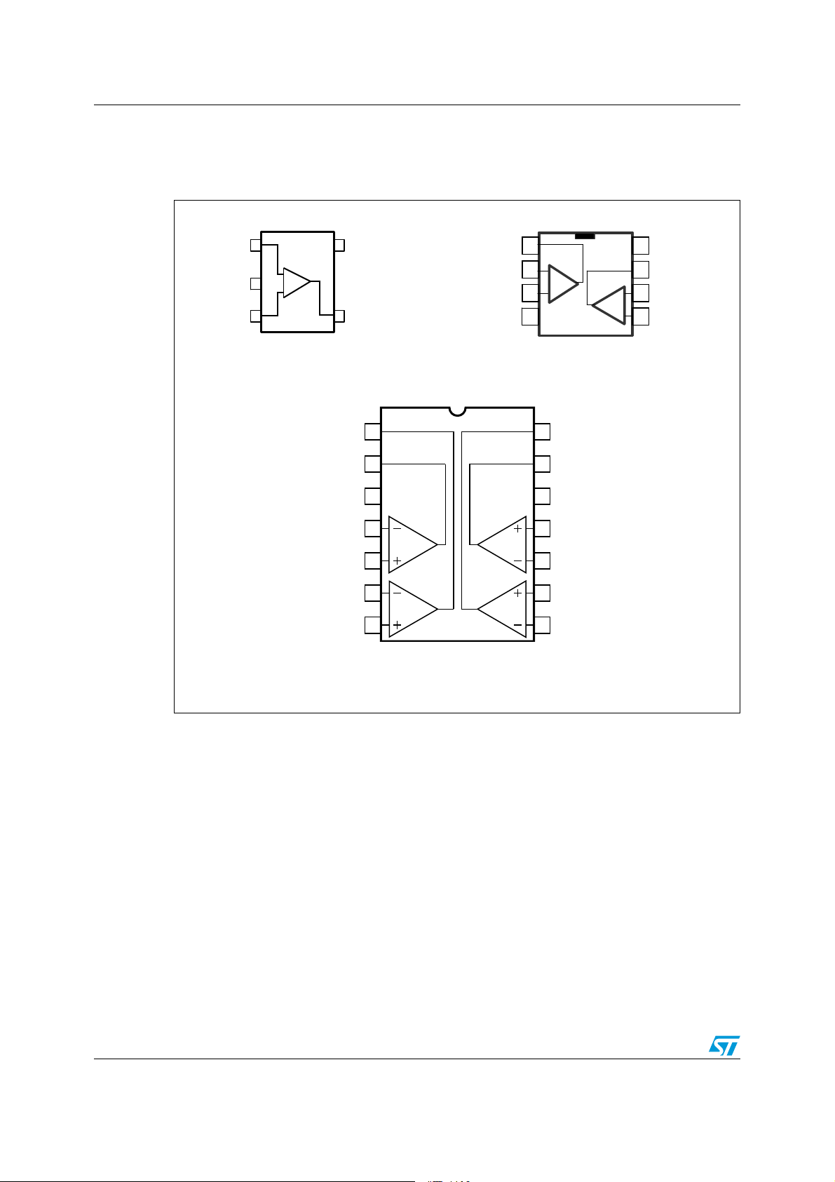
Package pin connections LMV331, LMV393, LMV339
1 Package pin connections
Figure 1. Pin connections for each package (top view)
IN +
1
+
2
VCC -
IN -
-
3
LMV331
SOT23-5 / SC70-5
VCC +
5
4OUT
OUT2
OUT1
VCC+
IN1-
IN1+
IN2-
IN2+
Out1
Out1
In1-
In1-
In1+
In1+
V
V
CC-
CC-
1
1
_
_
2
2
+
+
3
3
4
4
8
8
V
V
CC+
CC+
7
7
Out2
Out2
_
_
+
+
In2-
In2-
6
6
In2+
In2+
5
5
LMV393
SO-8 / MiniSO-8
1
2
3
4
5
6
14
OUT3
13
OUT4
VCC-
12
IN4+
11
IN4-
10
9
IN3+
87
IN3-
LMV339
SO14 / TSSOP14
2/17 Doc ID 16866 Rev 3
LMV331, LMV393, LMV339 Absolute maximum ratings and operating conditions
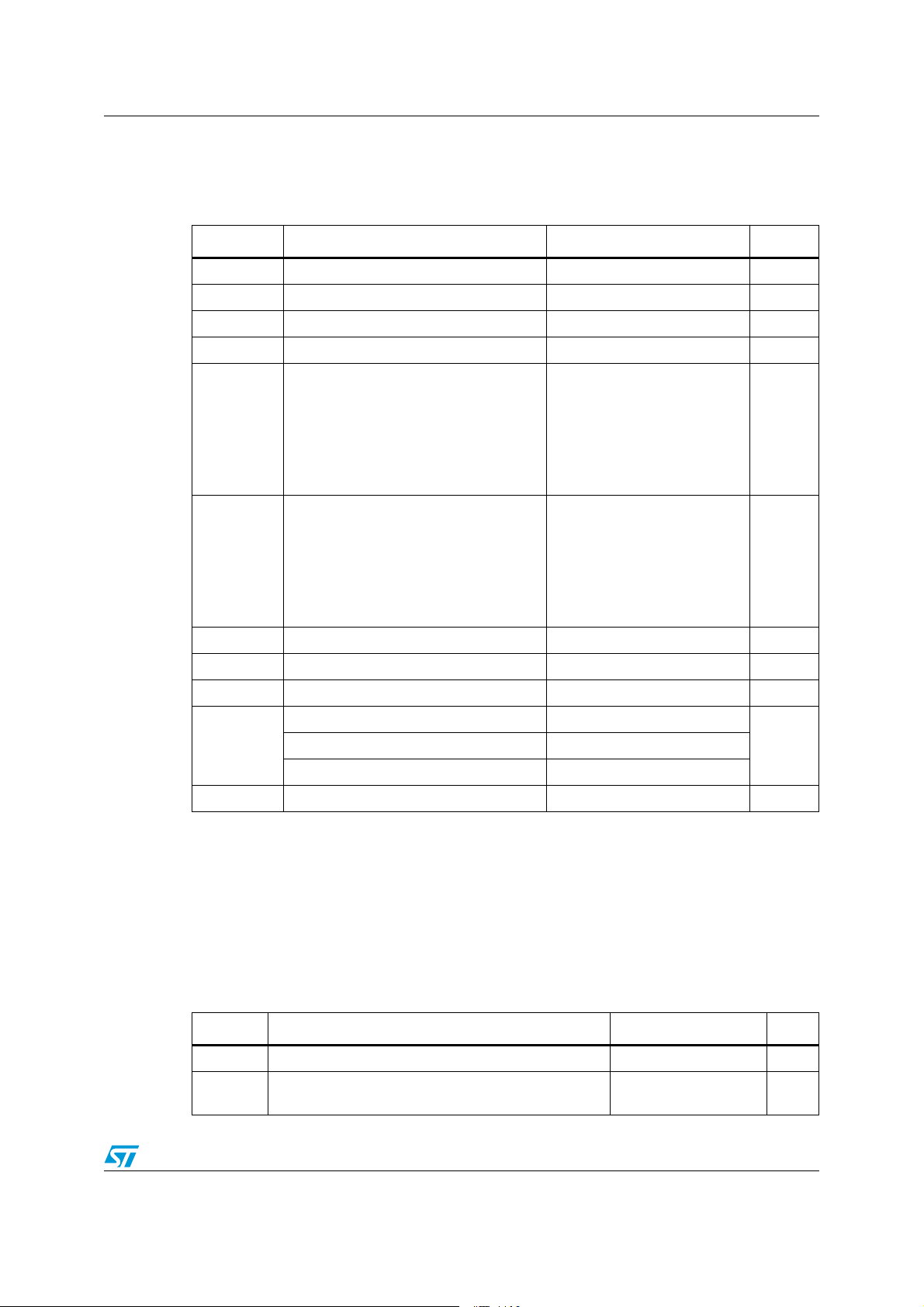
2 Absolute maximum ratings and operating conditions
Table 1. Absolute maximum ratings
Symbol Parameter Value Unit
V
V
V
V
R
R
T
T
LEAD
ESD
CC
out
thja
thjc
stg
T
Supply voltage
ID
IN
Differential input voltage ± 5.5 V
Input voltage range (VCC-) - 0.3 to (VCC+) + 0.3 V
Output voltage
Thermal resistance junction to ambient
SC70-5
SOT23-5
SO-8
MiniSO-8
SO14
TSSOP14
Thermal resistance junction to case
SC70-5
SOT23-5
SO-8
MiniSO-8
SO14
TSSOP14
Storage temperature -65 to +150 °C
j
Junction temperature 150 °C
Lead temperature (soldering 10 seconds) 260 °C
Human body model (HBM)
Charged device model (CDM)
Latch-up immunity 200 mA
(1)
(1)
(4)
(3)
(5)
(2)
(2)
5.5 V
5.5 V
205
250
125
190
105
100
172
81
40
39
31
32
2000
200
1500
°C/W
°C/W
VMachine model (MM)
1. All voltage values, except the differential voltage, are referenced to Vcc-.
2. Short-circuits can cause excessive heating. These values are typical.
3. Human body model: a 100 pF capacitor is charged to the specified voltage, then discharged through a
1.5 kΩ resistor between two pins of the device. This is done for all couples of connected pin combinations
while the other pins are floating.
4. Machine model: a 200 pF capacitor is charged to the specified voltage, then discharged directly between
two pins of the device with no external series resistor (internal resistor < 5 Ω). This is done for all couples of
connected pin combinations while the other pins are floating.
5. Charged device model: all pins and package are charged together to the specified voltage and then
discharged directly to ground through only one pin. This is done for all pins.
Table 2. Operating conditions
Symbol Parameter Value Unit
T
oper
V
Operating temperature range -40 to +85 °C
Supply voltage
CC
-40°C < T
< +85°C 2.7 to 5.0
amb
Doc ID 16866 Rev 3 3/17
V
Electrical characteristics LMV331, LMV393, LMV339
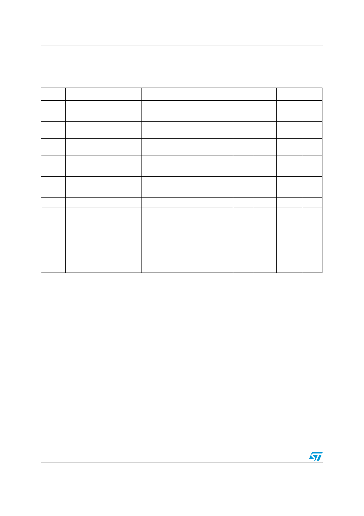
3 Electrical characteristics
Table 3. V
+
=+2.7V, V
CC
CC
-
=0V, T
= +25° C, full V
amb
range (unless otherwise specified)
ICM
Symbol Parameter Test conditions Min. Typ. Max. Unit
V
Input offset voltage 1 7 mV
IO
ΔV
Input offset voltage drift -40°C < T
IO
I
Input bias current
IB
I
Input offset current
IO
(2)
(2)
-40°C < T
-40°C < T
< +85°C 5 μV/°C
amb
25 250
< +85°C
amb
400
150
< +85°C
amb
150
-0.1
V
I
TP
TP
Common mode input voltage
ICM
V
Output voltage low I
OL
Output sink current V
SINK
I
Supply current No load, output high, V
CC
I
Output current leakage
OH
Propagation delay
HL
High to low output level
Propagation delay
LH
Low to high output level
= 1 mA 20 mV
SINK
= 1.5 V 5 47 mA
OUT
-40°C < T
=0V, RL=5.1kΩ, CL=50pF
V
ICM
Overdrive = 10 mV
Overdrive = 100 mV
= 0 V, RL = 5.1 kΩ, CL = 50 pF
V
ICM
Overdrive = 10 mV
Overdrive = 100 mV
< +85°C
amb
2.0
=0V 20 100 μA
ICM
0.003
1
300
200
550
400
(1)
nA
nA
V
μA
ns
ns
1. All values over the temperature range are guaranteed through correlation and simulation. No production tests have been
performed at the temperature range limits.
2. Maximum values include unavoidable inaccuracies of the industrial tests.
4/17 Doc ID 16866 Rev 3
LMV331, LMV393, LMV339 Electrical characteristics
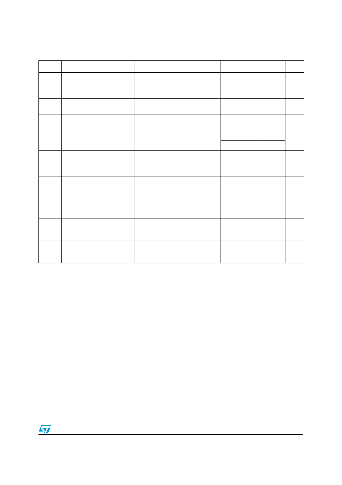
Table 4. V
CC
+
=+5V, V
CC
-
= 0 V, T
= +25°C, full V
amb
range (unless otherwise specified)
ICM
Symbol Parameter Test conditions Min. Typ. Max. Unit
V
ΔV
Input offset voltage
IO
Input offset voltage drift -40°C < T
IO
I
Input bias current
IB
I
Input offset current
IO
(2)
(2)
-40°C < T
-40°C < T
-40°C < T
< +85°C
amb
< +85°C 5 μV/°C
amb
< +85°C
amb
< +85°C
amb
17
9
25 250
400
250
150
-0.1
V
I
TP
Common mode input voltage
ICM
A
Voltage gain 20 50 V/mV
V
< 4 mA
I
V
Output voltage low
OL
Output sink current V
SINK
I
Supply current
CC
I
Output current leakage
OH
Propagation delay
HL
High to low output level
SINK
-40°C < T
< 1.5 V 10 93 mA
OUT
No load, output high, V
-40°C < T
-40°C < T
= 0 V, RL = 5.1 kΩ, CL = 50 pF
V
ICM
amb
amb
amb
< +85°C
< +85°C
< +85°C
ICM
= 0 V
Overdrive = 10 mV
Overdrive = 100 mV
4.2
50 400
25 120
0.003
375
275
700
150
1
(1)
mV
nA
nA
V
mV
μA
μA
ns
= 0 V, RL = 5.1 kΩ, CL = 50 pF
V
TP
1. All values over the temperature range are guaranteed through correlation and simulation. No production tests have been
2. Maximum values include unavoidable inaccuracies of the industrial tests.
Propagation delay
LH
Low to high output level
performed at the temperature range limits.
ICM
Overdrive = 10 mV
Overdrive = 100 mV
550
425
ns
Doc ID 16866 Rev 3 5/17
Electrical characteristics LMV331, LMV393, LMV339
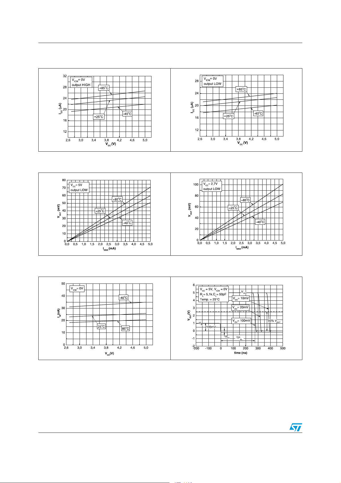
Figure 2. Supply current versus supply
voltage with output high
Figure 4. Output voltage versus output
current at 5 V supply
Figure 3. Supply current versus supply
voltage with output low
Figure 5. Output voltage versus output
current at 2.7 V supply
Figure 6. Input bias current versus supply
voltage
Figure 7. Response time versus overdrive
with negative transition, V
CC
= 5 V
6/17 Doc ID 16866 Rev 3
 Loading...