

ST LMV321L, LMV358L, LMV324L User Manual
LMV321L, LMV358L, LMV324L
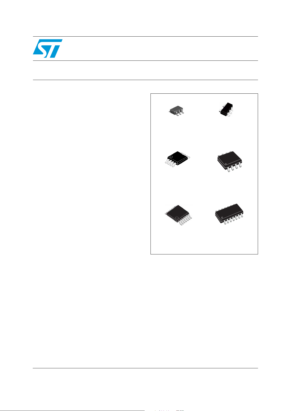
TSSOP14
SO-8
SO-14
SC70-5
MiniSO-8
SOT23-5
Low-power, general-purpose operational amplifier
Features
■ Low power consumption: 250 µA max at 5 V
■ Low offset voltage: 7 mV max at 25 °C
■ Industrial temperature range: -40 °C to +125 °C
■ Low supply voltage: 2.7 V - 5.5 V
■ Gain bandwidth product: 1.3 MHz
■ Tiny packages
Applications
■ Battery-powered applications
■ Portable devices
■ Signal conditioning
■ Active filtering
■ Medical instrumentation
Datasheet − production data
Description
The LMV321L, LMV358L and LMV324L are
single, dual and quad operational amplifiers with
rail-to-rail output capabilities. They are specifically
designed to operate at low voltages (2.7 to 5 V)
with enhanced performances compared to the
industry standard LM3xx series.
The LMV321L, LMV358L and LMV324L are
offered in tiny packages, allowing the devices to
be used in small portable electronic applications
and be placed closer to the actual signal.
The LMV321L, LMV358L and LMV324L are
complete cost-effective solutions for designs
where cost is of primary importance.
May 2012 Doc ID 023066 Rev 1 1/19
This is information on a product in full production.
www.st.com
19
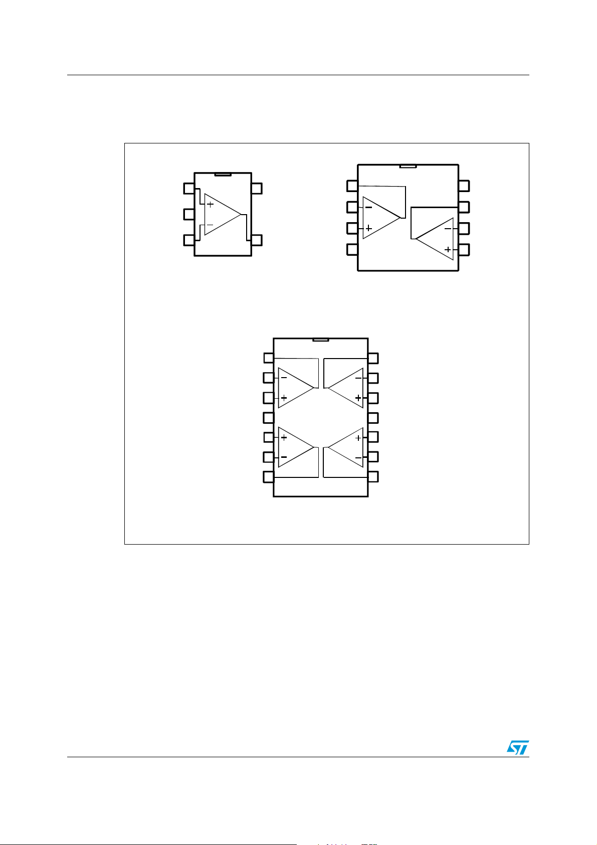
Package pin connections LMV321L, LMV358L, LMV324L
SC70-5 / SOT23-5
SO-8 / MiniSO-8
3
4
5
6
7
14
10
8
TSSOP14 / SO-14
1 Package pin connections
Figure 1. Pin connections for each package (top view)
1
In+
2
Vcc-
In- Out
3
5
4
Out1
In1-
In1+
In2+
In2-
Out2
Vcc+
1
2
4Vcc+
Out1
In1-
In1+
1
2
3
4Vcc-
Out4
-
13
In
In4+
12
Vcc-
11
In3+
9
In3-
Out3
Vcc+
8
Out2
7
In2-
6
5In2+
2/19 Doc ID 023066 Rev 1
LMV321L, LMV358L, LMV324L Absolute maximum ratings and operating conditions
2 Absolute maximum ratings and operating conditions
Table 1. Absolute maximum ratings (AMR)
Symbol Parameter Value Unit
(4)
(1)
(8)
(2)
(7)
(9)
(3)
(5)(6)
V
CC-
6V
±V
CC
- 0.3 to V
+ 0.2 V
CC+
V
10 mA
°C/W
4000
250
VMM: machine model
1300
V
CC
V
V
I
in
T
stg
Supply voltage
Differential input voltage
id
Input pins (IN+ and IN- pins) voltage
in
Input current
Storage temperature -65 to +150 °C
Thermal resistance junction to ambient
SC70-5 205
SOT23-5 250
R
thja
MiniSO-8 190
SO-8 125
TSSOP14 100
SO-14 105
T
Maximum junction temperature 150 °C
j
HBM: human body model
ESD
CDM: charged device model
Latch-up immunity 200 mA
1. All voltage values, except differential voltage, are with respect to network ground terminal.
2. Differential voltages are the non-inverting input terminal with respect to the inverting input terminal.
3. VCC-Vin must not exceed 6 V, Vin must not exceed 6 V.
4. Input current must be limited by a resistor in series with the inputs.
5. Short-circuits can cause excessive heating and destructive dissipation.
are typical values.
6. R
th
7. Human body model: 100 pF discharged through a 1.5 kΩ resistor between two pins of the device, done for
all couples of pin combinations with other pins floating.
8. Machine model: a 200 pF cap is charged to the specified voltage, then discharged directly between two
pins of the device with no external series resistor (internal resistor < 5 Ω), done for all couples of pin
combinations with other pins floating.
9. Charged device model: all pins plus package are charged together to the specified voltage and then
discharged directly to the ground.
Table 2. Operating conditions
Symbol Parameter Value Unit
T
V
V
CC
icm
oper
Supply voltage 2.7 to 5.5 V
Common mode input voltage range V
CC-
- 0.2 to V
- 1 V
CC+
Operating free-air temperature range -40 to +125 °C
Doc ID 023066 Rev 1 3/19
Electrical characteristics LMV321L, LMV358L, LMV324L
nV
Hz
----------- -
pA
Hz
----------- -
3 Electrical characteristics
Table 3. Electrical characteristics at V
Symbol Parameter Conditions Min. Typ. Max. Unit
DC performance
and R
= 2.7 V with V
connected to VCC/2 (unless otherwise specified)
L
CC+
= 0 V, V
CC-
= VCC/2, T
icm
= 25° C,
amb
V
ΔV
io
I
I
CMRR Common mode rejection ratio
Input offset voltage 1 7 mV
io
/ΔT Input offset voltage drift
Input offset current V
io
Input bias current V
ib
(1)
-40°C < T< 125°C 5 μV/°C
out=Vcc
out=Vcc
(1)
Vic = 0V to Vcc-1V, V
/2 0.5 30 nA
/2 27 60 nA
= V
out
/2 70 75 dB
cc
RL=10kΩ, high level 2.6 2.69 V
V
I
CC
Output swing
O
Supply current (per channel) No load, V
=10kΩ, low level 65 180 mV
R
L
= V
out
/2 120 180 µA
CC
AC performance
GBP Gain bandwidth product RL>1MΩ, CL= 200 pF 1.3 MHz
Φ
G
SR Slew rate
e
i
1. CMRR (dB) = 20 log (ΔV
Phase margin RL>1MΩ, CL= 200 pF 60 degrees
m
Gain margin RL>1MΩ, CL= 200 pF 10 dB
m
>1MΩ, CL= 200 pF
R
L
V
= 0.5 V to VCC-0.5V
out
Equivalent input noise voltage
n
Equivalent input noise current f = 1 kHz 0.30
n
/ΔVio).
icm
f=1kHz
f = 10 kHz
0.6 V/μs
31
20
Table 4. Electrical characteristics at V
R
connected to VCC/2 (unless otherwise specified)
L
= 5 V with V
CC+
CC-
= 0 V, V
= VCC/2, T
icm
= 25° C, and
amb
Symbol Parameter Conditions Min. Typ. Max. Unit
DC performance
17
V
ΔV
io
I
I
CMRR Common mode rejection ratio
Input offset voltage
io
/ΔT Input offset voltage drift
Input offset current
io
Input bias current
ib
(1)
-40°C < T< 125°C 9
-40°C < T< 125°C 5 μV/°C
V
out=Vcc
/2 0.5 30
-40°C < T< 125°C 50
V
out=Vcc
/2 27 60
-40°C < T< 125°C 110
(2)
Vic = 0 V to Vcc-1V,V
out
= V
/2 72 75 dB
cc
4/19 Doc ID 023066 Rev 1
mV
nA
nA
LMV321L, LMV358L, LMV324L Electrical characteristics
nV
Hz
----------- -
pA
Hz
----------- -
Table 4. Electrical characteristics at V
R
connected to VCC/2 (unless otherwise specified) (continued)
L
= 5 V with V
CC+
= 0 V, V
CC-
= VCC/2, T
icm
= 25° C, and
amb
Symbol Parameter Conditions Min. Typ. Max. Unit
SVRR Supply voltage rejection ratio Vcc = 2.7 to 5 V 72 79 dB
= 2 kΩ,
R
L
V
= 0.5V to (VCC-0.5V)
A
Large signal voltage gain
vd
out
90 100
-40°C < T< 125°C 80
=10kΩ 4.90 4.99
R
L
R
=10kΩ, -40°C < T< 125°C 4.80
V
OH
V
I
out
I
CC
Output swing high level
Output swing low level
OL
Output short circuit current
Supply current (per channel)
L
=2kΩ 4.70 4.96
R
L
R
=2kΩ, -40°C < T< 125°C 4.60
L
=10kΩ 65 180
R
L
R
=10kΩ, -40°C < T< 125°C 280
L
R
=2kΩ 120 300
L
=2kΩ, -40°C < T< 125°C 400
R
L
Sinking, V
Sourcing, V
No load, V
= V
out
CC
= 0 V 60 70
out
= VCC/2 130 250
out
35 43
-40°C < T< 125°C 350
dB
V
mV
mA
µA
AC performance
GBP Gain bandwidth product R
F
Φ
G
Unity gain frequency RL>1MΩ, CL= 200 pF 1 MHz
u
Phase margin RL>1MΩ, CL= 200 pF 60 degrees
m
Gain margin RL>1MΩ, CL= 200 pF 10 dB
m
SR Slew rate
e
i
1. See Chapter 4.4: Input offset voltage drift over temperature.
CMRR (dB) = 20 log (ΔV
2.
Equivalent input noise voltage
n
Equivalent input noise current f = 1 kHz 0.30
n
/ΔVio).
icm
>1MΩ, CL= 200 pF 1.3 MHz
L
>1MΩ, CL= 200 pF
R
L
= 0.5 V to VCC-0.5V
V
out
f=1kHz
f=10kHz
0.7 V/μs
30
20
Doc ID 023066 Rev 1 5/19
Electrical characteristics LMV321L, LMV358L, LMV324L
3.03.54.04.55.05.5
0.00
0.05
0.10
0.15
0.20
T=25°C
T=-40°C
T=85°C
Vicm=Vcc/2
Supply Current (mA)
Supply Voltage (V)
0.0 0.5 1.0 1.5 2.0 2.5 3.0 3.5 4.0
0.0
0.1
0.2
0.3
0.4
0.5
0.6
0.7
0.8
0.9
1.0
T=25°C
T=-40°C
T=125°C
Vcc=5V
Input Offse t Voltage (mV)
Input Common Mode Voltage (V)
0.00.0 0.5 1.01.0 1.5 2.02.0 2.5
-30
-20-20
-10
00
10
2020
30
Source
Vid=1V
Sink
Vid=-1V
T=-40°C
T=25°C
T=125°C
T=-40°C
Vcc=2.7V
T=125°C
T=25°C
Output Current (mA)
Output Voltage (V)
0.00.0 0.5 1.01.0 1.5 2.02.0 2.5 3.03.0 3.5 4.04.0 4.5 5.05.0
-100-100
-75
-50-50
-25
00
25
5050
75
100100
Source
Vid=1V
Sink
Vid=-1V
T=-40°C
T=25°C
T=125°C
T=-40°C
Vcc=5V
T=125°C
T=25°C
Output Current (mA)
Output Voltage (V)
2.8 3.03.0 3.3 3.53.5 3.8 4.04.0 4.3 4.54.5 4.8 5.05.0 5.3 5.55.5
-100-100
-75
-50-50
-25
00
25
5050
75
100100
Source
Vid=1V
Sink
Vid=-1V
T=-40°C
T=25°C
T=85°C
T=-40°C
Vicm=Vcc/2
T=85°C
T=25°C
Output Current (mA)
Supply Voltage (V)
10k 100k 1M 10M
-20
-10
0
10
20
30
40
-270
-225
-180
-135
-90
-45
0
Gain (dB)
Frequency (Hz)
Gain
Phase
Vcc=5V
Vicm=2.5V
Rl=50k
Ω
Cl=200pF
Gain=-100
T=125°C
T=-40°C
T=25°C
Phase (°)
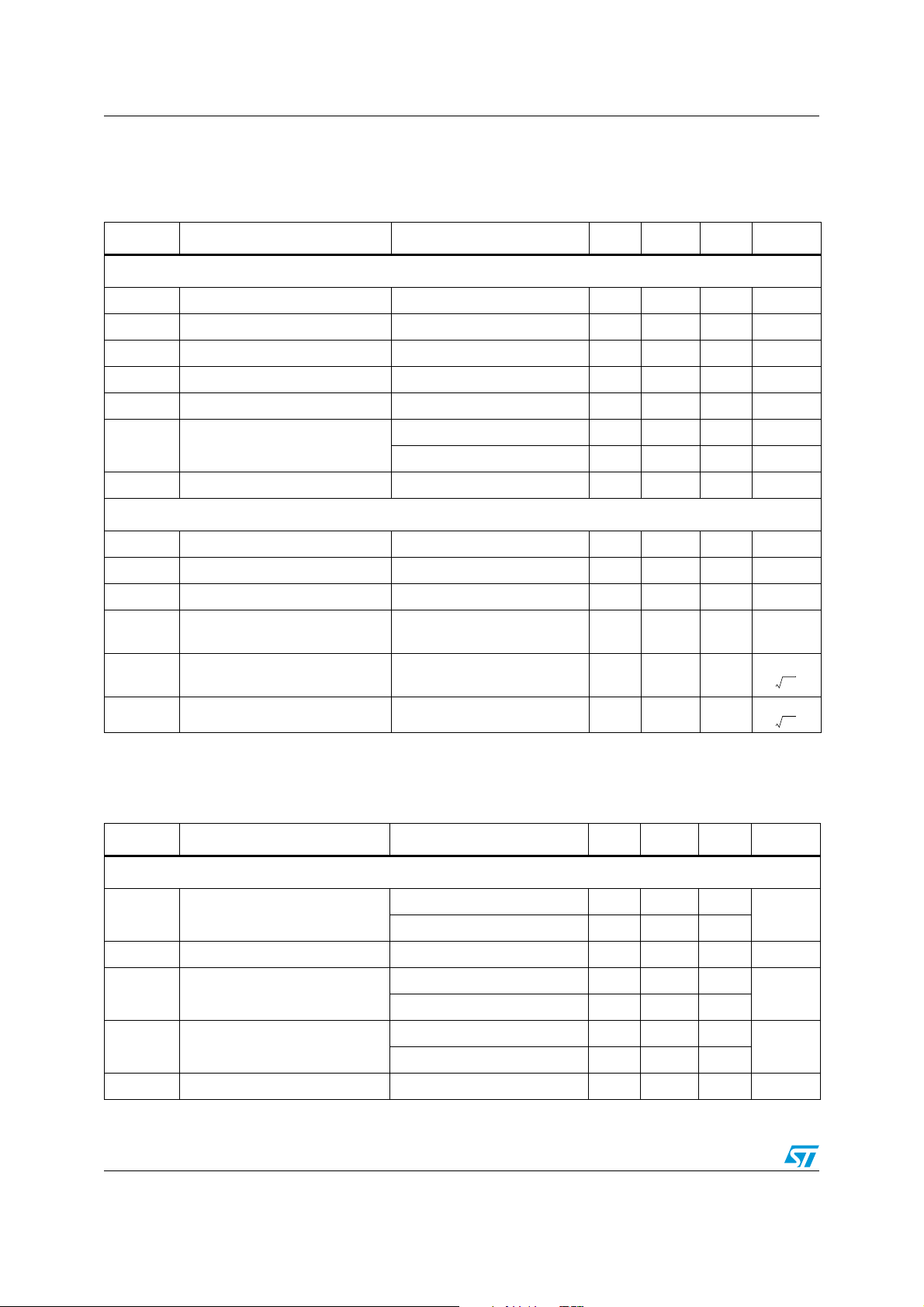
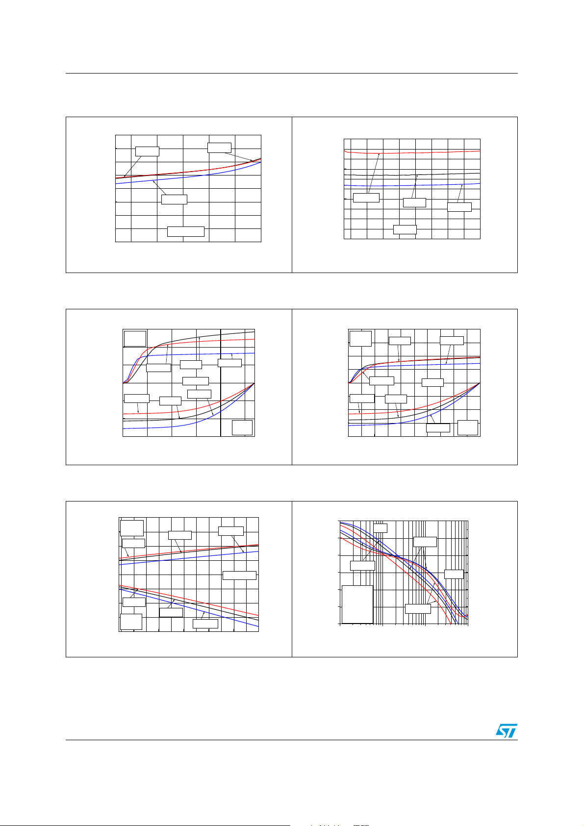
Figure 2. Supply current vs. supply voltage at
V
= VCC/2
icm
Figure 4. Output current vs. output voltage at
V
= 2.7 V
CC
Figure 3. Input offset voltage vs. input
common mode voltage at V
CC
= 5 V
Figure 5. Output current vs. output voltage at
VCC = 5 V
Figure 6. Output current vs. supply voltage at
V
icm
6/19 Doc ID 023066 Rev 1
= VCC/2
Figure 7. Voltage gain and phase with
Cl = 200 pF
 Loading...