

ST LM139, LM239, LM339 User Manual
Low-power quad voltage comparators
Features
■ Wide single supply voltage range or dual
supplies for all devices: +2 to +36 V or ±1 V to
±18 V
■ Very low supply current (1.1 mA) independent
of supply voltage
■ Low input bias current: 25 nA typ
■ Low input offset current: ±5 nA typ
■ Low input offset voltage: ±1 mV typ
■ Input common-mode voltage range includes
ground
■ Low output saturation voltage: 250 mV typ;
(I
= 4 mA)
SINK
■ Differential input voltage range equal to the
supply voltage
■ TTL, DTL, ECL, MOS, CMOS compatible
outputs
Description
This family of devices consists of four
independent precision-voltage comparators with
an offset voltage specification as low as 2 mV
maximum for LM339A, LM239A and LM139A.
Each comparator has been designed specifically
to operate from a single power supply over a wide
range of voltages. Operation from split power
supplies is also possible.
These comparators also have a unique
characteristic in that the input common mode
voltage range includes ground even though
operated from a single power supply voltage.
LM139, LM239, LM339
N
DIP14
(Plastic package)
D
SO-14
(Plastic micropackage)
P
TSSOP14
(Thin shrink small outline package)
Q
QFN16 3x3
(Plastic micropackage)
July 2011 Doc ID 2159 Rev 3 1/19
www.st.com
19
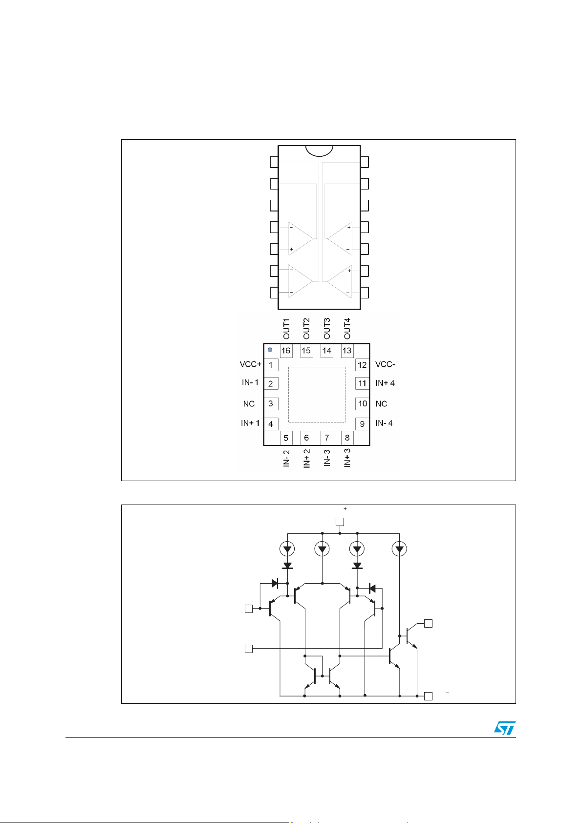
Pin and schematic diagram LM139, LM239, LM339
1 Pin and schematic diagram
Figure 1. Pin connections (top view)
Output2
Output1
V
CC
Inverting input1
N on-inverting input1
Inverting input2
N on-inverting input2
1
2
+
3
4
5
6
7
14
Output3
Output4
13
12
11
10
9
8
-
V
CC
Non-inverting input4
Inverting input4
Non-inverting input3
Inverting input3
Figure 2. Schematic diagram (1/4 LM139)
3.5μA
Non-inverting
input
2/19 Doc ID 2159 Rev 3
Inverting
input
V
CC
100 μA
3.5μA
100μA
V
O
V
CC
LM139, LM239, LM339 Absolute maximum ratings and operating conditions
2 Absolute maximum ratings and operating conditions
Table 1. Absolute maximum ratings
Symbol Parameter Value Unit
V
V
V
R
R
T
T
LEAD
ESD
1. Short-circuits from the output to V
maximum output current is approximately 20 mA independent of the magnitude of V
Supply voltage ±18 or 36 V
CC
Differential input voltage ±36 V
ID
Input voltage -0.3 to +36 V
IN
Output short-circuit to ground
Thermal resistance junction to ambient
(1)
(2)
DIP14
thja
SO-14
TSSOP14
QFN16 3x3
Thermal resistance junction to case
(2)
DIP14
thjc
SO-14
TSSOP14
QFN16 3x3
Storage temperature range -65 to +150 °C
stg
Junction temperature +150 °C
T
j
Infinite
80
105
100
45
33
31
32
14
Lead temperature (soldering 10 seconds) 260 °C
Human body model (HBM)
Charged device model (CDM)
(3)
(4)
(5)
+
can cause excessive heating and eventual destruction. The
CC
500
100
1500
+
CC
.
°C/W
°C/W
2. Short-circuits can cause excessive heating. These values are typical.
3. Human body model: a 100 pF capacitor is charged to the specified voltage, then discharged through a
1.5 kΩ resistor between two pins of the device. This is done for all couples of connected pin combinations
while the other pins are floating.
4. Machine model: a 200 pF capacitor is charged to the specified voltage, then discharged directly between
two pins of the device with no external series resistor (internal resistor < 5 Ω). This is done for all couples of
connected pin combinations while the other pins are floating.
5. Charged device model: all pins and the package are charged together to the specified voltage and then
discharged directly to the ground through only one pin. This is done for all pins.
VMachine model (MM)
Doc ID 2159 Rev 3 3/19

Absolute maximum ratings and operating conditions LM139, LM239, LM339
Table 2. Operating conditions (T
Symbol Parameter Value Unit
amb
= 25° C)
V
V
T
Supply voltage
CC
Common mode input voltage range 0 to (V
ICM
Operating free-air temperature range
– LM139, LM139A
oper
– LM239, LM239A
– LM339, LM339A
2 to 32
±1 to ±16
+
- 1.5) V
CC
-55, +125
-40, +105
0, +70
V
°C
4/19 Doc ID 2159 Rev 3
LM139, LM239, LM339 Electrical characteristics
3 Electrical characteristics
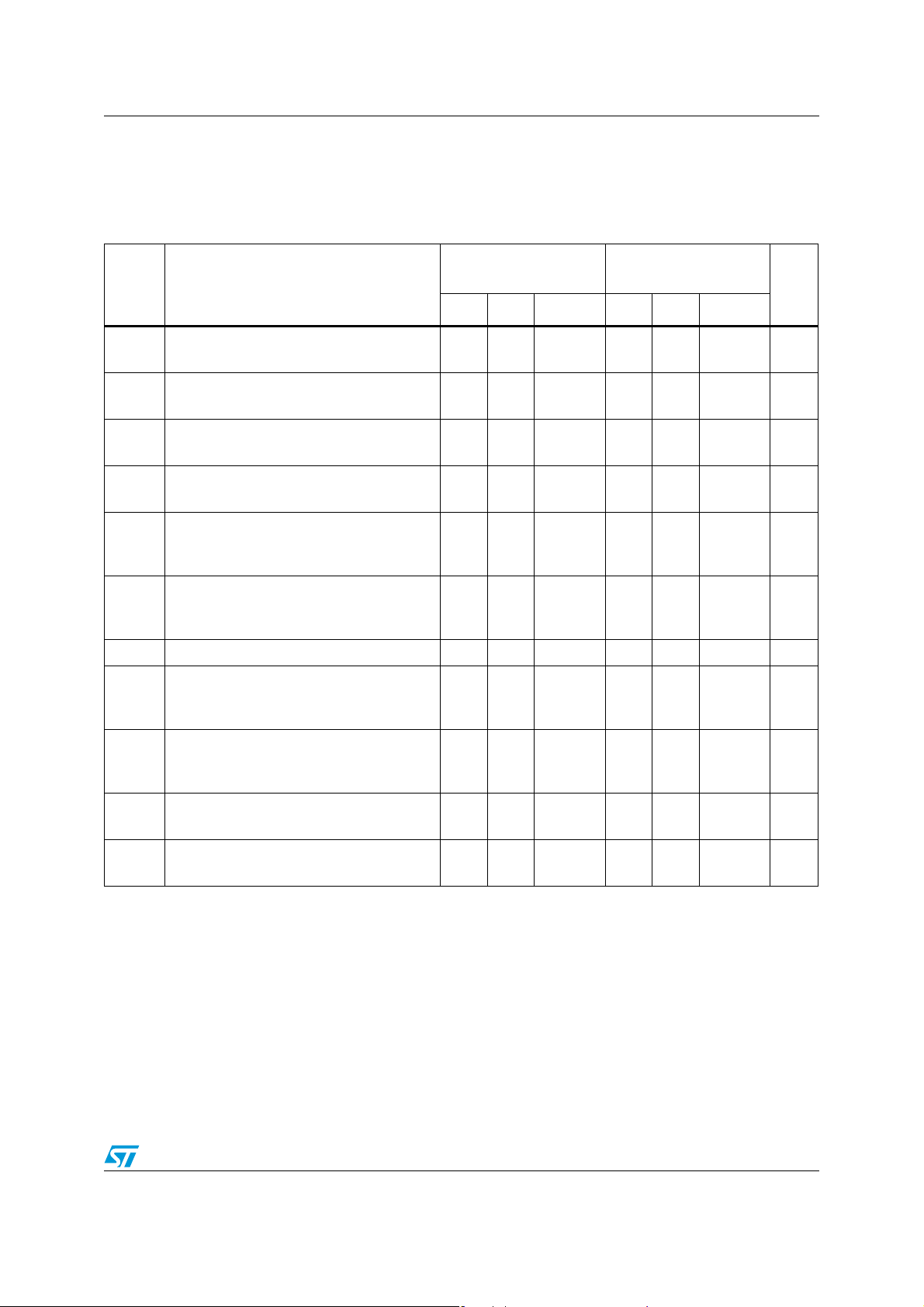
Table 3. Electrical characteristics at V
(unless otherwise specified)
Symbol Parameter
V
I
I
A
I
CC
V
ICM
V
V
I
OH
I
SINK
t
Input offset voltage
IO
T
≤ T
min
amb
Input offset current
IO
T
≤ T
min
amb
Input bias current (I+ or I-)
IB
T
≤ T
min
amb
Large signal voltage gain
VD
= 15 V, RL = 15 kΩ, Vo = 1 V to 11 V 50 200 50 200 V/mV
V
CC
Supply current (all comparators)
= +5 V, no load
V
CC
VCC = +30 V, no load
Input common mode voltage range
V
= 30 V
CC
T
≤ T
min
amb
Differential input voltage
ID
Low level output voltage
= -1 V, I
OL
V
ID
T
≤ T
min
amb
High level output current
= Vo = 30 V, VID = 1 V
V
CC
≤ T
T
min
amb
Output sink current
VID= 1 V, Vo = 1.5 V 6 16 6 16 mA
Response time
re
= 5.1 kΩ connected to V
R
L
≤ T
≤ T
≤ T
≤ T
SINK
≤ T
≤ T
max
max
max
max
= 4 mA
max
max
(5)
(1)
(2)
(3)
(4)
+
CC
+
= +5 V, V
CC
LM139A - LM239A
-
= GND, T
CC
= +25° C
amb
LM139 - LM239
LM339A
Min. Typ. Max. Min Typ. Max.
12
4
325
100
25 100
300
1.1
1.3
0
0
V
V
CC
CC
V
2
2.5
+
-1.5
+
-200
+
CC
250 400
700
0.1
1
1.3 1.3 μs
LM339
159mV
550
150
25 250
400
1.1
1.3
2
2.5
+
V
-1.5
CC
+
-2
V
CC
+
V
CC
250 400
700
0.1
1
Unit
nA
nA
mA
V
V
mV
nA
μA
Doc ID 2159 Rev 3 5/19

Electrical characteristics LM139, LM239, LM339
Table 3. Electrical characteristics at V
+
= +5 V, V
CC
-
= GND, T
CC
= +25° C
amb
(unless otherwise specified) (continued)
LM139A - LM239A
Symbol Parameter
LM339A
Min. Typ. Max. Min Typ. Max.
Large signal response time
trel
= 5.1 kΩ connected to V
R
L
= +1.4 V 300 300 ns
V
(ref)
1. At output switch point, Vo ≈ 1.4 V, V
2. The direction of the input current is out of the IC due to the PNP input stage. This current is essentially constant,
independent of the state of the output, so no loading charge exists on the reference of input lines.
3. The input common-mode voltage of either input signal voltage should not be allowed to go negative by more than 0.3 V.
The upper end of the common-mode voltage range is V
damage.
4. Positive excursions of input voltage may exceed the power supply level. As long as the other voltage remains within the
common-mode range, the comparator will provide a proper output state. The low input voltage state must not be less than
-0.3 V (or 0.3 V below the negative power supply, if used).
5. The response time specified is for a 100 mV input step with 5 mV overdrive. For larger overdrive signals, 300 ns can be
obtained.
+
, el = TTL,
CC
+
from 5 V to 30 V, and over the full common-mode range (0 V to V
CC
+
-1.5 V, but either or both inputs can go to +30 V without
CC
LM139 - LM239
LM339
CC
+
-1.5 V).
Unit
6/19 Doc ID 2159 Rev 3
 Loading...