

ST LM137, LM337 User Manual
Features
LM137
LM337
Three-terminal adjustable negative voltage regulators
■ Output voltage adjustable down to V
■
1.5 A guaranteed output current
■ 0.3%/V typical load regulation
■ 0.01%/V typical line regulation
■ Current limit constant with temperature
■ Ripple rejection: 77 dB
■ Standard 3-lead transistor packages
■ Excellent thermal regulation: 0.002%/V
■ 50 ppm/°C temperature coefficient
REF
Description
The LM137 series are adjustable 3-terminal
negative voltage regulators capable of supplying
in excess -1.5 A over a -1.2 to -37 V output
voltage range. They are exceptionally easy to use
and require only two external resistors to set the
output voltage. Further, both line and load
regulation are better than standard fixed
regulators. Also, LM137 regulators are supplied in
standard transistor packages which are easily
mounted and handled. In addition to higher
performance than fixed regulators, the LM137
series offer full overload protection available only
in integrated circuits. Included on the chip are
current limit, thermal overload protection and safe
area protection. All overload protection circuitry
remains fully functional even if the adjustment
terminal is disconnected.
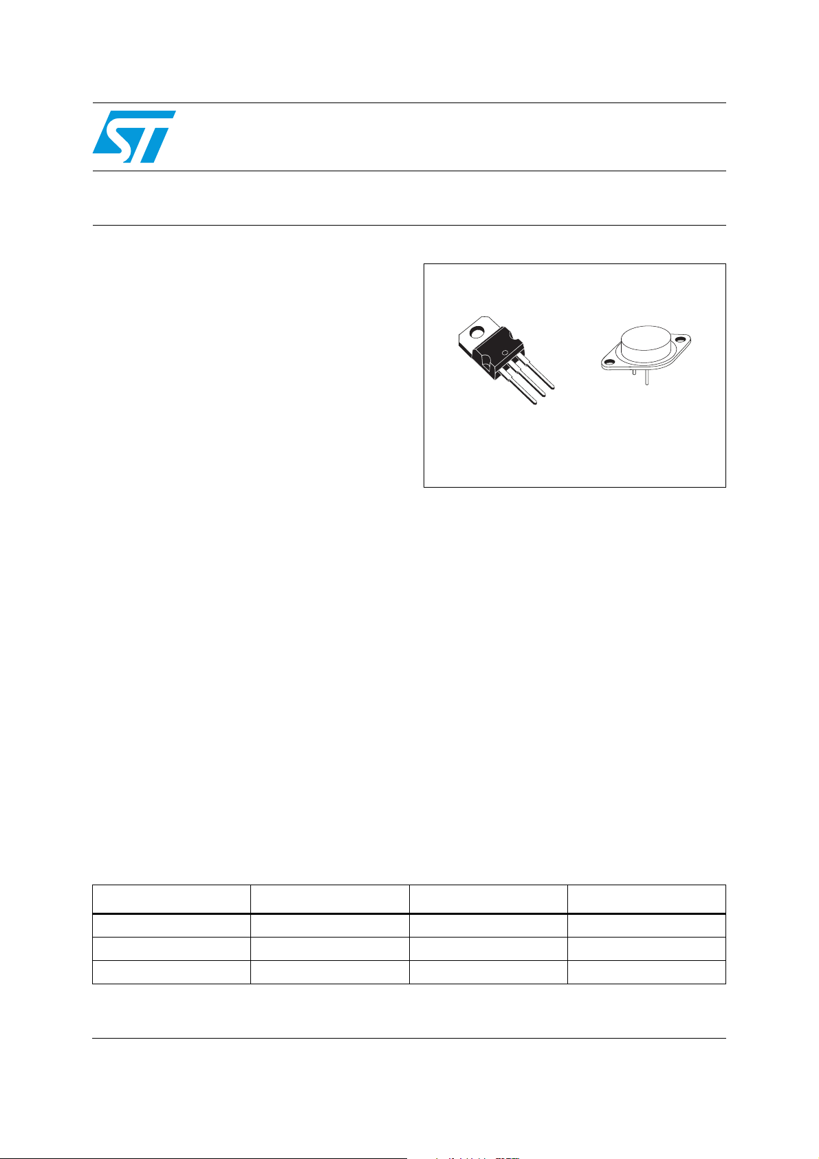
TO-220
TO-3
Table 1. Device summary
Part numbers Order codes Packages Temperature range
LM137 LM137K TO-3 - 55 °C to 150 °C
LM337 LM337K TO-3 0 °C to 125 °C
LM337 LM337SP TO-220 0 °C to 125 °C
October 2011 Doc ID 2167 Rev 4 1/18
www.st.com
18

Contents LM137, LM337
Contents
1 Diagram . . . . . . . . . . . . . . . . . . . . . . . . . . . . . . . . . . . . . . . . . . . . . . . . . . . 3
2 Pin configuration . . . . . . . . . . . . . . . . . . . . . . . . . . . . . . . . . . . . . . . . . . . . 4
3 Maximum ratings . . . . . . . . . . . . . . . . . . . . . . . . . . . . . . . . . . . . . . . . . . . . 5
4 Electrical characteristics . . . . . . . . . . . . . . . . . . . . . . . . . . . . . . . . . . . . . 6
5 Typical characteristics . . . . . . . . . . . . . . . . . . . . . . . . . . . . . . . . . . . . . . . 8
6 Thermal regulation . . . . . . . . . . . . . . . . . . . . . . . . . . . . . . . . . . . . . . . . . 10
7 Typical application . . . . . . . . . . . . . . . . . . . . . . . . . . . . . . . . . . . . . . . . . 11
8 Package mechanical data . . . . . . . . . . . . . . . . . . . . . . . . . . . . . . . . . . . . 14
9 Revision history . . . . . . . . . . . . . . . . . . . . . . . . . . . . . . . . . . . . . . . . . . . 17
2/18 Doc ID 2167 Rev 4
LM137, LM337 Diagram
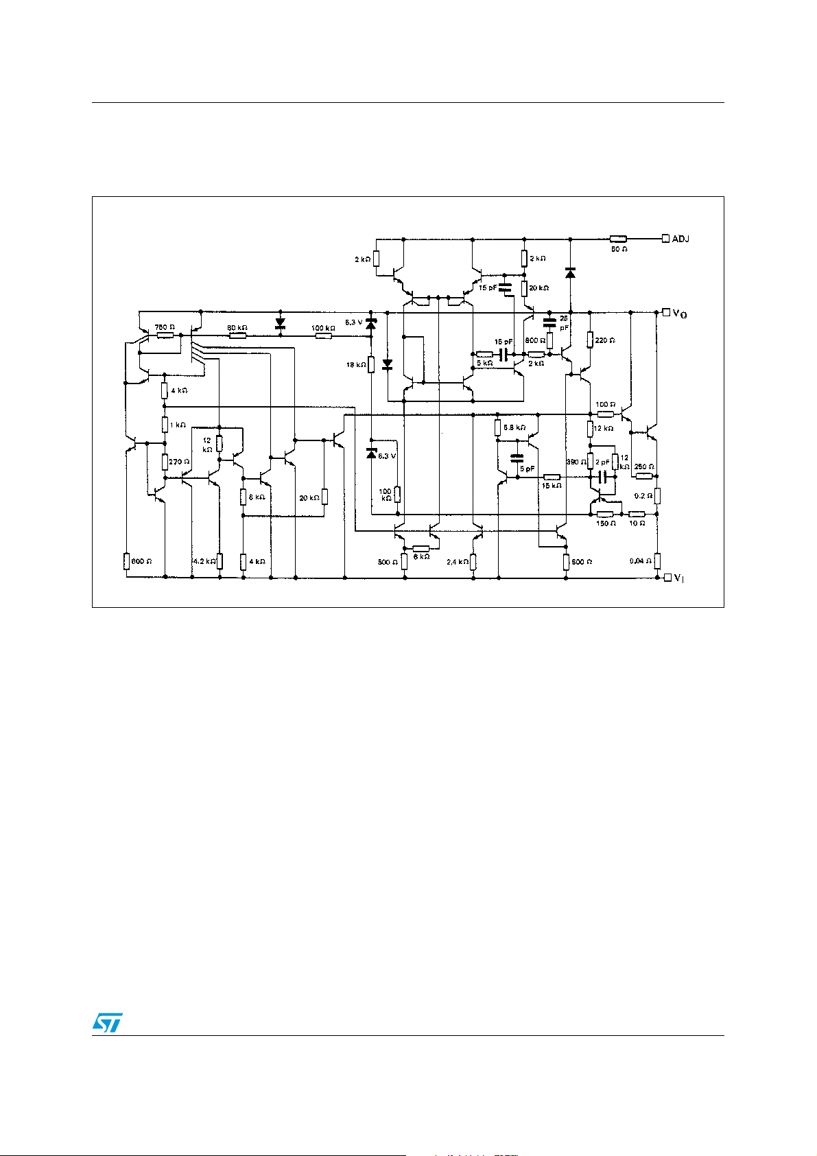
1 Diagram
Figure 1. Schematic diagram
Doc ID 2167 Rev 4 3/18
Pin configuration LM137, LM337
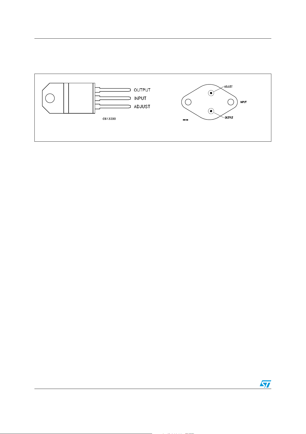
2 Pin configuration
Figure 2. Pin connections (top view)
TO-220
TO-3
4/18 Doc ID 2167 Rev 4
LM137, LM337 Maximum ratings
3 Maximum ratings
Table 2. Absolute maximum ratings
Symbol Parameter Value Unit
- VOInput output voltage differential 40 V
V
I
I
P
T
STG
T
OP
Note: Absolute maximum ratings are those values beyond which damage to the device may occur.
Table 3. Thermal data
Output current 1.5 A
O
Power dissipation Internally limited
D
Storage temperature range - 65 to 150 °C
Operating junction temperature range
LM137 - 55 to 150
LM337 0 to 125
Functional operation under these condition is not implied.
°C
Symbol Parameter TO-220 TO-3 Unit
R
R
thJC
thJA
Thermal resistance junction-case max. 3 4 °C/W
Thermal resistance junction-ambient max. 70 35 °C/W
Doc ID 2167 Rev 4 5/18
Electrical characteristics LM137, LM337
4 Electrical characteristics
TJ = -55 to 150 °C, VI - VO = 5 V, IO = 0.5 A unless otherwise specified.
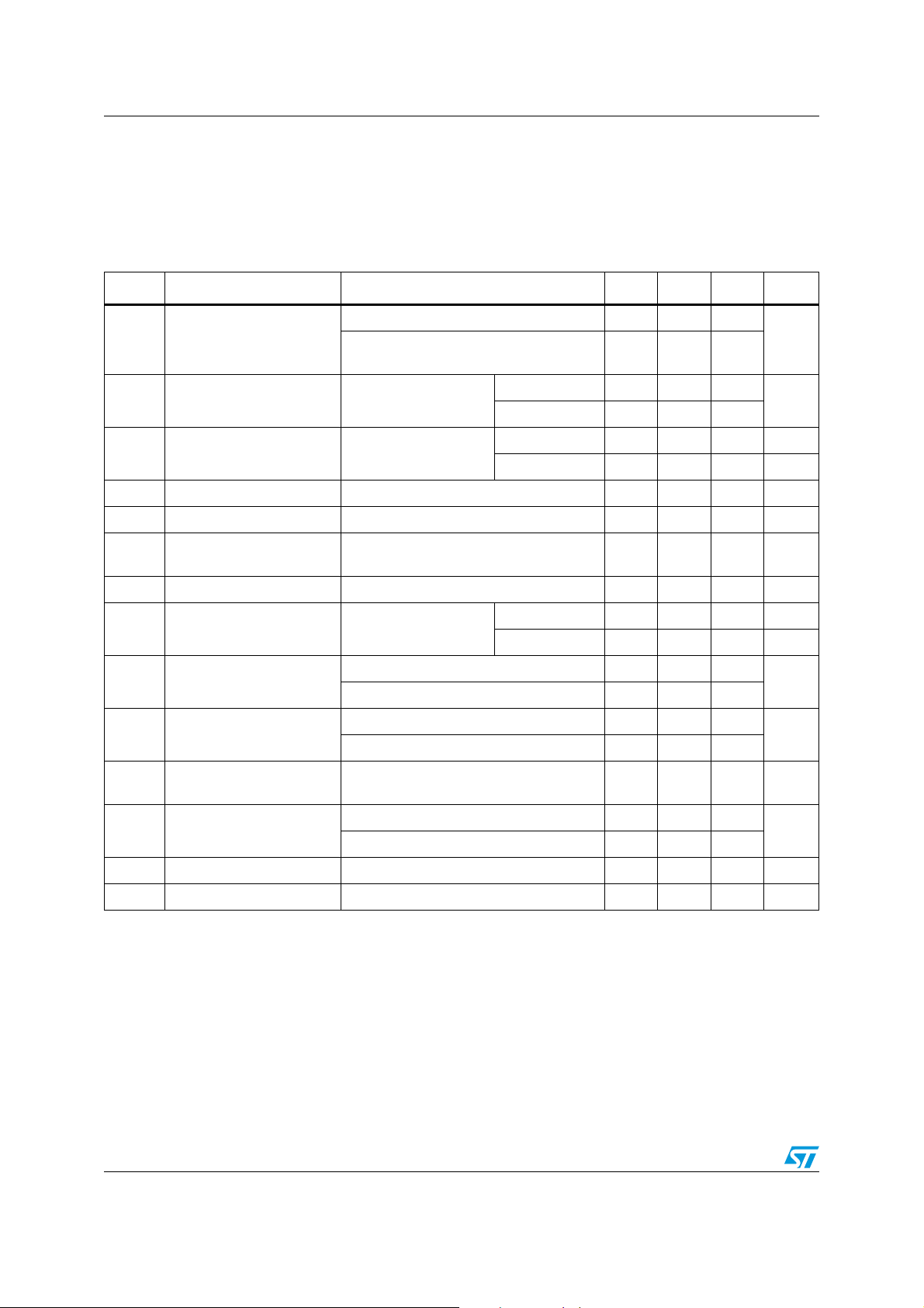
Table 4. Electrical characteristics of LM137
Symbol Parameter Test conditions Min. Typ. Max. Unit
Ta = 25°C -1.225 -1.25 -1.275
V
K
I
ΔI
K
|I
O(min)
V
R
K
K
1. Regulation is measured at constant junction temperature, using pulse testing with a low duty cycle. Changes in output
Reference voltage
REF
K
VI
VO
Line regulation
Load regulation
(1)
(1)
Thermal regulation T
Adjustment pin current 65 100 µA
ADJ
Adjustment pin current
ADJ
change
K
VI
VO
Line regulation
Load regulation
(1)
(1)
| Minimum load current
I
Short circuit output current
OS
RMS output noise
NO
(% of V
Ripple rejection ratio
VF
Temperature stability 0.6 %
VT
Long term stability Ta = 125°C, 1000 H 0.3 1 %
VH
voltage due to heating effects are covered under the specification for thermal regulation.
)
O
|V
- VO| = 3 to 40 V, TJ = T
I
|IO| = 10mA to |I
O(max)
| P ≤ P
Ta = 25°C
- VO| = 3 to 40 V
|V
I
Ta = 25°C
|IO| = 10mA to |I
= 25°C, pulse 10 ms 0.002 0.02 %/W
a
O(max)
|
Ta = 25°C, |IO| = 10 mA to |I
|VI - VO| = 3 to 40 V
to T
min
max
max
-1.2 -1.25 -1.3
IO = 0.1 A 0.01 0.02
= 20 mA 0.01 0.02
I
O
| ≤ 5 V 15 25 mV
|V
O
| ≥ 5 V 0.3 0.5 %
|V
O
|
O(max)
25µA
|VI - VO| = 3 to 40 V 0.02 0.05 %/V
|VO| ≤ 5 V 20 50 mV
|IO| = 10mA to |I
|V
- VO| ≤ 40 V 2.5 5
I
- VO| ≤ 10 V 1.2 3
|V
I
|V
- VO| ≤ 15 V 1.5 2.2
I
- VO| = 40 V, TJ =25°C 0.24 0.4
|V
I
= 25°C, f = 10 Hz to 10 kHz 0.003 %
T
a
V
= -10 V, f = 120 Hz 60
O
= 10 µF 66 77
C
ADJ
O(max)
|
| ≥ 5 V 0.3 1 %
|V
O
V
%/V
mA
A
dB
= 0 to 150 °C unless otherwise specified.
T
J
6/18 Doc ID 2167 Rev 4
 Loading...