

Low Power Quad Operational Amplifiers
■ Wide gain bandwidth: 1.3MHz
■ Large voltage gain: 100dB
■ Very low supply current/ampli: 375µA
■ Low input bias current: 20nA
■ Low input offset voltage: 3mV max.
■ Low input offset current: 2nA
■ Wide power supply range:
Single supply: +3V to +30V
Dual supplies: ±1.5V to ±15V
■ Input common-mode voltage range
includes ground
■ ESD internal protection: 2KV
LM224A - LM324A
N
DIP14
(Plastic Package)
Description
These circuits consist of four independent, high
(Plastic Micropackage)
D
SO-14
gain, internally frequency compensated
operational amplifiers. They operate from a single
power supply over a wide range of voltages.
Operation from split power supplies is also
possible and the low power supply current drain is
independent of the magnitude of the power supply
voltage.
All the pins are protected against electrostatic
discharges up to 2KV (as a consequence, the
(Thin Shrink Small Outline Package)
P
TSSOP-14
input voltages must not exceed the magnitude of
+
or V
V
CC
CC
-
.)
Order Codes
Part Number Temperature Range Package Packaging
LM224AN
LM224AD/ADT SO Tube or Tape & Reel
LM224APT
LM324AN
LM324AD/ADT SO Tube or Tape & Reel
LM324APT
-40°C, +105°C
(Thin Shrink Outline Package)
0°C, +70°C
(Thin Shrink Outline Package)
DIP Tube
TSSOP
DIP Tube
TSSOP
Tape & Reel
Tape & Reel
February 2005 Revision 2 1/16
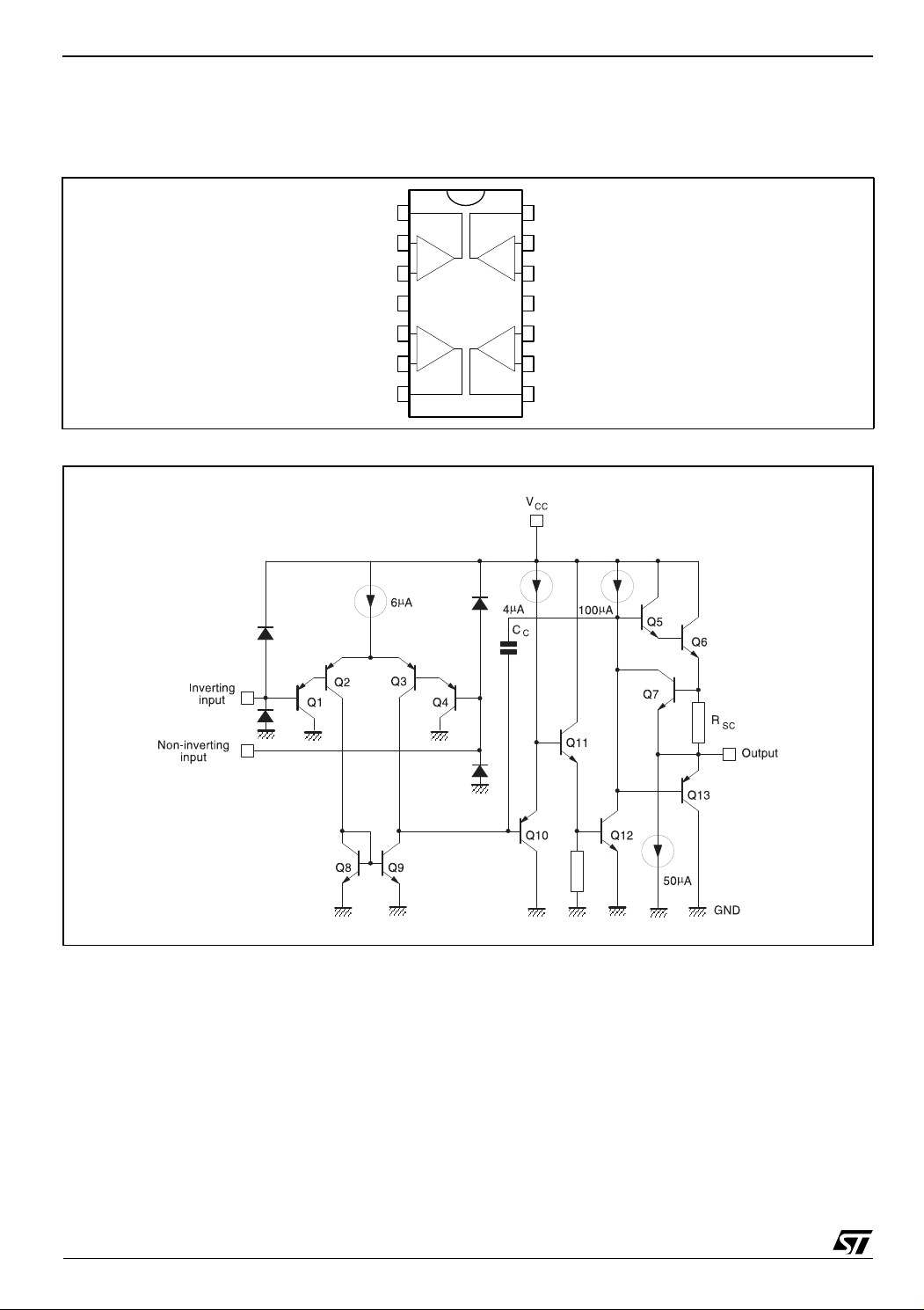
LM224A-LM324A Pin & Schematic Diagram
1 Pin & Schematic Diagram
Figure 1: Pin connections (top view)
V
CC
1
2
3
+
4
5
6
7
Output 1
Inverting Input 1
Non-inverting Input 1
Non-inverting Input 2
Inverting Input 2
Output 2
Figure 2: Schematic diagram (1/4 LM124A)
14
Output 4
Inverting Input 4
13
-
+
+
-
-
+
+
-
Non-inverting Input 4
12
-
V
11
CC
10
Non-inverting Input 3
9
Inverting Input 3
8
Output 3
2/16
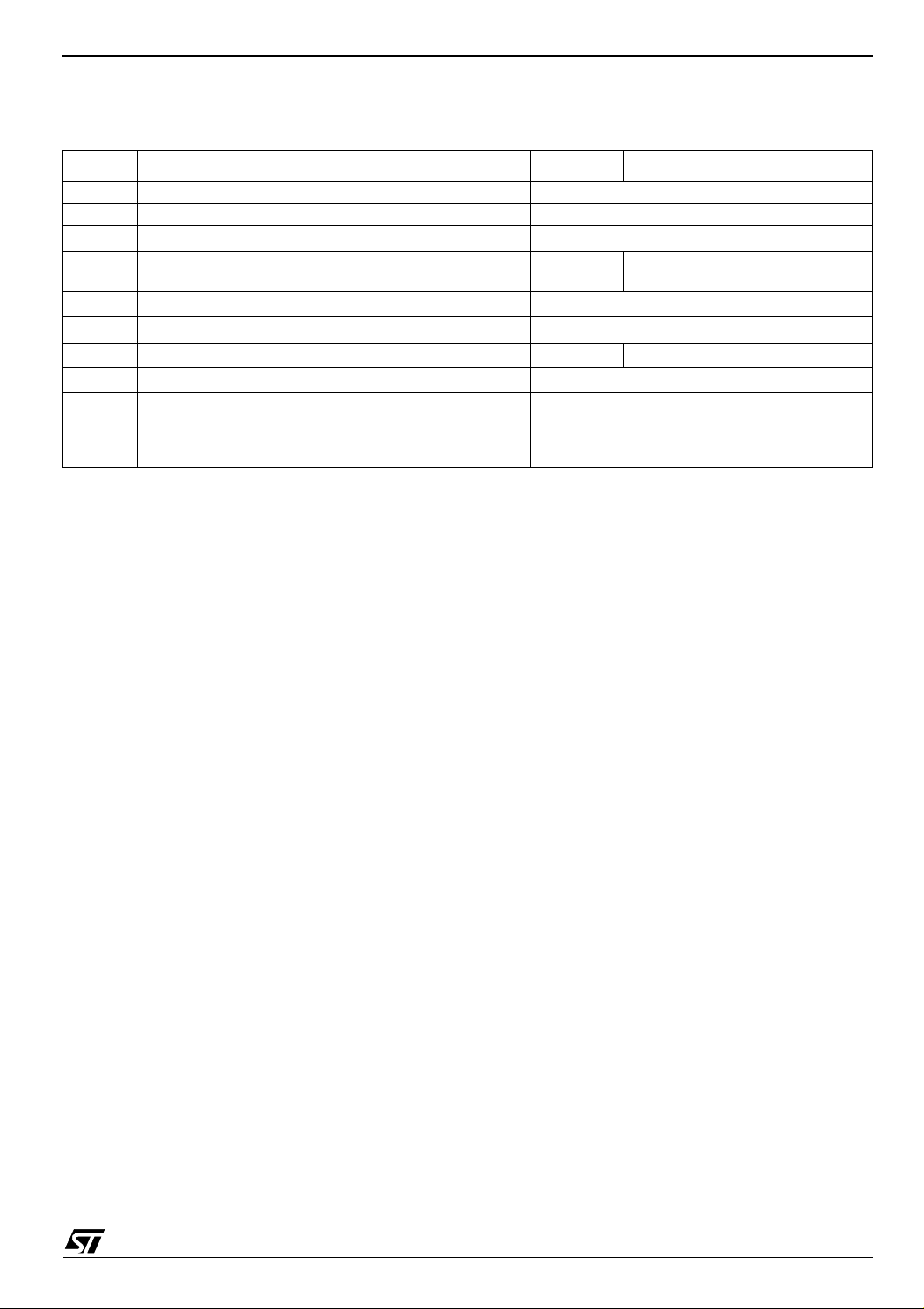
Absolute Maximum Ratings LM224A-LM324A
2 Absolute Maximum Ratings
Table 1: Key parameters and their absolute maximum ratings
Symbol Parameter LM124A LM224A LM324A Unit
VCC Supply voltage ±16 or 32 V
Vi Input Voltage -0.3 to Vcc + 0.3 V
V
Differential Input Voltage
id
P
Power DissipationN Suffix
tot
D Suffix
Output Short-circuit Duration
3
T
I
oper
T
Input Current
in
Operating Free-air Temperature Range
Storage Temperature Range
stg
Thermal Resistance Junction to Ambient
R
thja
SO14
TSSOP14
DIP14
1) Either or both input voltages must not exceed the magnitude of V
2) Short-circuits from the output to VCC can cause excessive heating if VCC > 15V. The maximum output current is approximately 40mA
independent of the magnitude of V
3) This input current only exists when the voltage at any of the input leads is driven negative. It is due to the collector-base junction of the
input PNP transistor becoming forward biased and thereby acting as input diodes clamps. In addition to this diode action, there is also
NPN parasitic action on the IC chip. this transistor action can cause the output voltages of the op-amps to go to the V
to ground for a large overdrive) for the time duration than an input is driven negative.
This is not destructive and normal output will set up again for input voltage higher than -0.3V.
1
32 V
500 500
400
2
Infinite
50 mA
-55 to +125 -40 to +105 0 to +70 °C
-65 to +150 °C
103
100
66
+
-
or V
CC
.
CC
. Destructive dissipation can result from simultaneous short-circuit on all amplifiers.
CC
500
400
voltage level (or
CC
mW
mW
°C/W
3/16
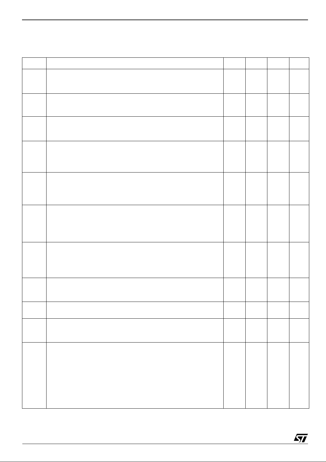
LM224A-LM324A Electrical Characteristics
3 Electrical Characteristics
Table 2: V
+
= +5V, V
CC
Symbol Parameter Min. Typ. Max. Unit
-
= Ground, Vo = 1.4V, T
CC
= +25°C (unless otherwise specified
amb
V
I
io
I
ib
A
vd
SVR
I
CC
V
icm
CMR
I
source
I
sink
V
OH
Input Offset Voltage - note 1
= +25°C
io
T
T
amb
min
≤ T
amb
≤ T
max
Input Offset Current
T
= +25°C
amb
≤ T
T
min
amb
≤ T
max
Input Bias Current - note
T
= +25°C
amb
≤ T
T
min
amb
≤ T
max
Large Signal Voltage Gain
+
V
= +15V, RL = 2kΩ, Vo = 1.4V to 11.4V
CC
= +25°C
T
amb
≤ T
T
min
amb
≤ T
max
Supply Voltage Rejection Ratio (R
+
= 5V to 30V
V
CC
= +25°C
T
amb
≤ T
T
min
amb
≤ T
max
Supply Current, all Amp, no load
= +25°C VCC = +5V
T
amb
= +30V
V
CC
≤ T
T
V
min
CC
amb
= +30V
≤ T
max VCC
Input Common Mode Voltage Range
V
= +30V - note
CC
T
= +25°C
amb
≤ T
T
min
amb
≤ T
max
Common Mode Rejection Ratio (R
= +25°C
T
amb
≤ T
T
min
amb
≤ T
max
Output Current Source (Vid = +1V)
= +15V, Vo = +2V 20 40 70
V
CC
Output Sink Current (Vid = -1V)
= +15V, Vo = +2V
V
CC
= +15V, Vo = +0.2V
V
CC
High Level Output Voltage
V
= +30V
CC
= +25°C RL = 2kΩ
T
amb
T
≤ T
≤ T
amb
max
= +25°C RL = 10kΩ
≤ T
≤ T
amb
max
T
T
min
amb
min
VCC = +5V, RL = 2kΩ
T
= +25°C
amb
≤ T
T
min
amb
≤ T
max
23
mV
5
nA
220
40
2
nA
20 100
200
V/mV
50
100
25
≤ 10kΩ)
s
65
110
dB
65
mA
3
= +5V
≤ 10kΩ)
s
70
0.7
1.5
0.8
1.5
0
0
80
1.2
3
1.2
3
V
V
-
CC
1.5
-2
V
CC
dB
60
mA
10
12
20
50
mA
µA
V
26
27
26
27
28
27
3.5
3
4/16
Electrical Characteristics LM224A-LM324A
Table 2: V
+
= +5V, V
CC
-
= Ground, Vo = 1.4V, T
CC
= +25°C (unless otherwise specified
amb
Symbol Parameter Min. Typ. Max. Unit
Low Level Output Voltage (R
= +25°C
VOL
SR
GBP
THD
e
n
DV
io
DI
Iio
V
o1/Vo2
1) Vo = 1.4V, Rs = 0Ω, 5V < V
2) The direction of the input current is out of the IC. This current is essentially constant, independent of the state of the output so no loading
change exists on the input lines.
3) The input common-mode voltage of either input signal voltage should not be allowed to go negative by more than 0.3V. The upper end
of the common-mode voltage range is V
4) Due to the proximity of external components insure that coupling is not originating via stray capacitance between these external parts.
This typically can be detected as this type of capacitance increases at higher frequences.
T
amb
≤ T
T
min
amb
≤ T
max
Slew Rate
V
= 15V, Vi = 0.5 to 3V, RL = 2kΩ, CL = 100pF, unity Gain
CC
Gain Bandwidth Product
= 30V, f =100kHz,Vin = 10mV, RL = 2kΩ, CL = 100pF
V
CC
Total Harmonic Distortion
f = 1kHz, A
= 20dB, RL = 2kΩ, Vo = 2V
v
Equivalent Input Noise Voltage
f = 1kHz, R
= 100Ω, VCC = 30V
s
Input Offset Voltage Drift
Input Offset Current Drift
Channel Separation - note 4
≤ f ≤ 20kHZ
1kHz
+
< 30V, 0 < Vic < V
CC
= 10kΩ)
L
, C
= 100pF, VCC = 30V
pp
L
+
- 1.5V
CC
+
- 1.5V, but either or both inputs can go to +32V without damage.
CC
520
20
V/
0.4
MHz
1.3
0.015
40
730
------------
µV/°C
10 200 pA/°C
120
mV
µs
%
nV
Hz
dB
5/16
LM224A-LM324A Electrical Characteristics
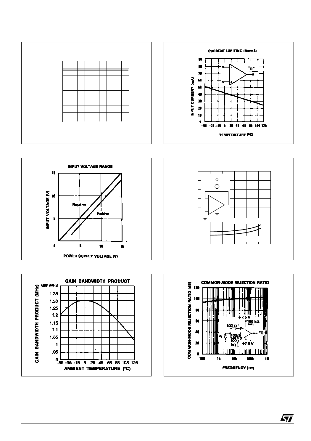
Figure 3: Input bias current vs. ambient
temperature
INPUT BIAS CURRENT
versus AMBIENT TEMPERATURE
IB (nA)
24
21
18
15
12
9
6
3
0
-55-35-15 5 25 45 65 85 105 125
AMBIENT TEMPERATURE (°C)
Figure 4: Input voltage range
Figure 6: Current limiting
Figure 7: Supply current
SUPPLY CURRENT
4
V
CC
I
D
mA
3
-
2
+
Figure 5: Gain bandwidth product
T
= 0°C to +125°C
1
SUPPLY CURRENT (mA)
0102030
POSITIVE SUPPLY VOLTAGE (V)
amb
T
amb
= -55°C
Figure 8: Common mode rejection ratio
6/16
 Loading...