

查询LM124供应商
LM124
LOW POWER QUAD OPERATIONAL AMPLIFIERS
.WIDEGAINBANDWIDTH : 1.3MHz
.INPUTCOMMON-MODE VOLTAGERANGE
INCLUDES GROUND
.LARGEVOLTAGE GAIN : 100dB
.VERYLOWSUPPLYCURRENT/AMPLI: 375µA
.LOW INPUT BIAS CURRENT : 20nA
.LOW INPUT OFFSETVOLTAGE: 5mV max.
(for more accurate applications,use theequivalent parts
LM124A-LM224A-LM324A which feature3mV max)
.LOW INPUT OFFSETCURRENT : 2nA
.WIDEPOWERSUPPLYRANGE:
SINGLESUPPLY: +3V TO +30V
DUALSUPPLIES: ±1.5VTO ±15V
LM224 - LM324
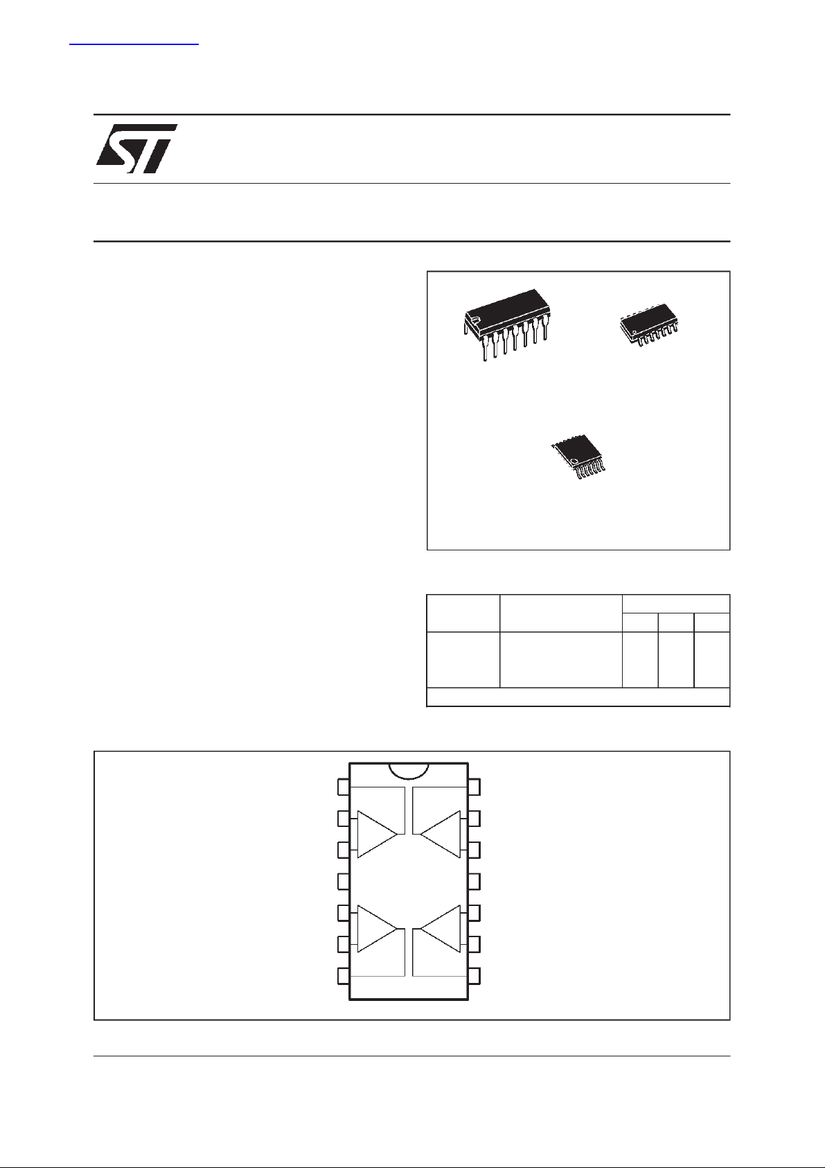
N
DIP14
(PlasticPackage)
(Thin Shrink Small Outline Package)
(PlasticMicropackage)
P
TSSOP14
D
SO14
DESC RIP TI ON
These circuits consist of four independent, high
gain,internally frequencycompensatedoperational
amplifiers.Theyoperatefromasinglepowersupply
over awide rangeof voltages.Operationfromsplit
powersupplies is also possible and the low power
supply current drain is independentof the magnitude of the power supplyvoltage.
PI N CONNECT I O NS ( top view)
Output 1
Inverting Input 1
Non-inverting Input 1
V
Non-inverting Input 2
Inverting Input 2
Output 2
CC
1
2
3
+
4
5
6
7
-
+
+
-
ORDER CODES
Part
Number
LM124 -55
LM224 -40
LM324 0
Example : LM224N
Output 4
14
Inverting Input 4
13
-
+
+
-
Non-inverting Input 4
12
V
11
Non-inverting Input 3
10
Inverting Input 3
9
Output 3
8
Temperature
Range
o
C, +125oC •••
o
C, +105oC •••
o
C, +70oC •••
-
CC
Package
NDP
June 1999
1/14
LM124 - LM224 - LM324
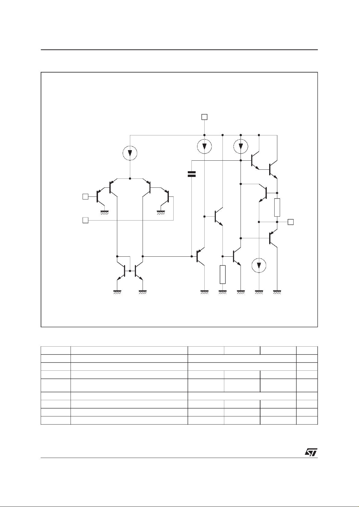
SCHE MATIC DI AG RAM (1/4 L M124)
V
CC
Inverting
input
Non-inverting
input
6µA
Q2
Q3
Q8 Q9
4µA
100µA
Q5
C
C
Q4Q1
Q7
Q6
R
SC
Q11
Output
Q13
Q10
Q12
50µA
GND
ABSOLUTE MAXIMUM RATINGS
Symbol Parameter LM124 LM224 LM324 Unit
V
V
V
P
- Output Short-circuit Duration - (note 1) Infinite
I
in
T
oper
T
stg
2/14
Supply Voltage ±16 or 32 V
cc
Input Voltage -0.3 to +32 V
i
Differential Input Voltage - (*) +32 +32 +32 V
id
Power Dissipation N Suffix
tot
D Suffix
500
-
500
400
Input Current – (note 6) 50 50 50 mA
Operating Free Air Temperature Range -55 to +125 -40 to +105 0 to +70
Storage Temperature Range -65 to +150 -65 to +150 -65 to +150
500
400
mW
mW
o
C
o
C
ELECTRICAL CHARACTERISTICS
V
CC
+
= +5V, V
–
= Ground, VO= 1.4V, T
CC
= +25oC (unless otherwise specified)
amb
LM124 - LM224 - LM324
Symbol Parameter
V
io
I
io
I
ib
A
vd
SVR Supply Voltage Rejection Ratio (R
I
CC
V
icm
Input Offset Voltage (note 3)
=+25oC
T
T
amb
min.
≤ T
amb
≤ T
max
.
LM324
LM324
Input Offset Current
=+25oC
T
amb
≤ T
≤ T
T
min.
amb
max
.
Input Bias Current (note 2)
=+25oC
T
amb
≤ T
≤ T
≤ T
≤ T
max
max
max
.
.
.
T
min.
amb
Large Signal Voltage Gain
+
= +15V, RL=2kΩ,VO= 1.4V to 11.4V)
(V
CC
=+25oC
T
amb
≤ T
T
min.
amb
+
= 5V to 30V)
(V
CC
=+25oC
T
amb
≤ T
T
min.
amb
Supply Current, all Amp, no load
=+25oCV
T
T
amb
min.
≤ T
amb
≤ T
.VCC= +5V
max
CC
V
CC
V
CC
Input Common Mode Voltage Range
= +30V) - (note 4)
(V
CC
=+25oC
T
amb
≤ T
T
min.
amb
≤ T
max.
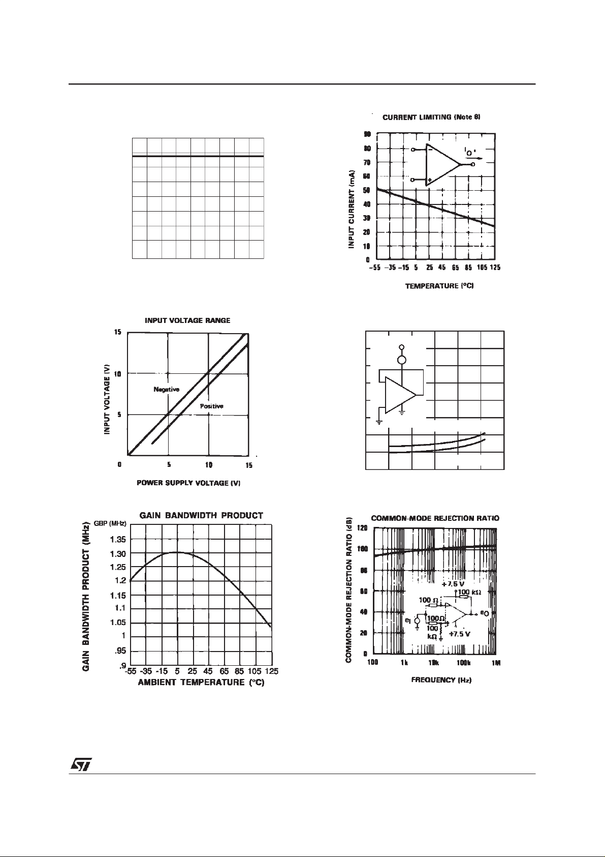
CMR Common-mode Rejection Ratio (R
=+25oC
T
amb
≤ T
≤ T
amb
max
= +15V, Vo= +2V 20 40 70
= +15V, Vo=+2V
= +15V, Vo= +0.2V
I
source
I
sink
T
min.
Output Current Source (Vid= +1V)
V
CC
Output Sink Current (Vid= -1V)
V
CC
V
CC
≤ 10kΩ)
S
= +5V
= +30V
= +30V
≤ 10kΩ)
S
LM124 - LM224 - LM324
Min. Typ. Max.
25
7
7
9
230
100
20 150
300
50
100
25
65
110
65
70
0.7
1.5
0.8
1.5
0
0
80
1.2
3
1.2
3
VCC-1.5
V
CC
60
10
12
20
50
Unit
mV
nA
nA
V/mV
dB
mA
V
-2
dB
mA
mA
µA
3/14
LM124 - LM224 - LM324
ELECTRICAL CHARACTERISTICS (continued)
Symbol Parameter
V
OH
V
OL
High Level Output Voltage
= +30V)
(V
CC
= +25oCR
T
amb
. ≤ T
T
min
= +25oCR
T
amb
. ≤ T
T
min
= +5V, RL=2kΩ)
(V
CC
= +25oC
T
amb
. ≤ T
T
min
amb
amb
amb
≤ T
≤ T
≤ T
max
max
max
.
.
.
=2kΩ
L
= 10kΩ
L
Low Level Output Voltage (RL= 10kΩ)
= +25oC
T
amb
. ≤ T
T
min
amb
≤ T
max
.
SR Slew Rate
= 15V, VI= 0.5 to 3V, RL=2kΩ,CL= 100pF,
V
CC
unity gain) 0.4
GBP Gain Bandwidth Product
= 30V, f = 100kHz, Vin= 10mV
V
CC
=2kΩ,CL= 100pF 1.3
R
L
THD Total Harmonic Distortion
f = 1kHz, A
CL= 100pF, VCC= 30V 0.015
e
n
DV
DI
IO
1/VO2 Channel Separation (note 5)
V
O
Notes : 1. Short-circuits from the output to VCCcan cause excessive heati ng if VCC> 15V. The maximum output current
Equivalent Input Noise Voltage
f = 1kHz, R
Input Offset Voltage Drift 7 30 µV/oC
io
Input Offset Current Drift 10 200 pA/oC
1kHz ≤ f ≤ 20kHz 120
is approximately 40mA i ndependent of the m agnitude of V
neous short-circuit on all amplifiers.
2. The dir ection of the input current is out of the IC . This current is essentially constant, independent of the state
of the output so no loading change exists on the i nput l ines.
= 1.4V, Rs=0Ω, 5V < V
3. V
o
4. The input common-mode voltage of either input signal voltage should not be allowed to go negative by more
than 0.3V. The upper end of the common-mode voltage range i s V
to + 32V wi thout damage.
5. Due t o the proximity of external components insure that coupling i s not originating via stray capacitance between these ext ernal parts. This typically can be detected as this t ype of capacitance increases at higher frequen ces.
6. This input current only exists when the voltage at any of t he i nput leads is driven negative. It is due to the
collector-base junction of the input PN P transistor becoming forward biased and thereby acting as input diodes clamps. I n addition to this diode action, there is also NPN parasitic act ion on the IC chip. t his t ransistor
act ion c a n cause t he ou t put voltag es of the Op- amps to go to the V
overdrive) for the time duration than an input i s dr iven negative.
This i s not destructive and normal output wi ll set up again f or input voltage higher than -0.3V.
= 20dB, RL=2kΩ,VO=2V
V
= 100Ω,VCC= 30V 40
s
+
<30V,0<Vic<V
CC
pp
CC
+
-1.5V
CC
LM124 - LM224 - LM324
Min. Typ. Max.
Unit
V
26
27
26
27
28
27
3.5
3
mV
520
20
V/µs
MHz
%
nV
√Hz
dB
. Des tr ucti v e diss ipation can r esult from sim ulta-
+
- 1.5V, but either or both inputs can go
CC
voltage l evel (or to ground for a large
CC
4/14
IB (nA)
INPUT BIAS CURRENT
versus AMBIENT TEMPERATURE
24
21
18
15
12
9
6
3
0
-55-35-15 5 25 45 65 85 105 125
AMBIENT TEMPERATURE
(
C)
LM124 - LM224 - LM324
SUPPLY CURRENT
4
V
CC
I
D
mA
3
-
2
1
SUPPLY CURRENT (mA)
+
T
=0 Cto+125 C
amb
T
=-55 C
amb
0102030
POSITIVE SUPPLY VOLTAGE (V)
5/14
 Loading...