

查询LM217M供应商
1.2 TO 37V ADJUSTABLE VOLTAGE REGULATOR
■ OUTPUTVOLTAGERANGE : 1.2 TO37V
■ OUTPUTCURRENT IN EXCESSOF 500 mA
■ LINEREGULATION TYP.0.01%
■ LOADREGULATIONTYP. 0.1%
■ THERMALOVERLOADPROTECTION
■ SHORTCIRCUIT PROTECTION
■ OUTPUTTRANSISTORSAFEAREA
COMPENSATION
■ FLOATINGOPERATIONFOR HIGH
VOLTAGEAPPLICATIONS
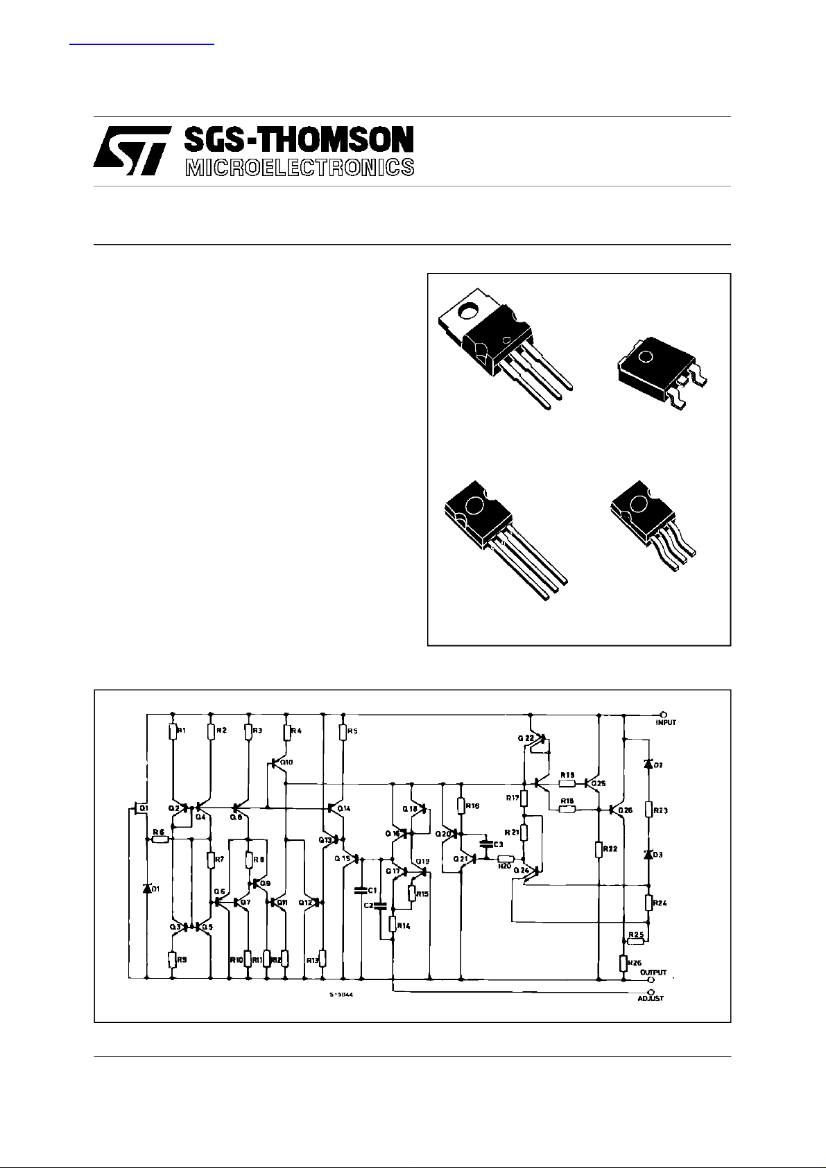
DESCRIPTION
The LM217M/LM317M are monolithic integrated
circuits in TO-220,DPAK, SOT-82 and SOT-194
packages intended for use as positive adjustable
voltageregulators.
They are designedto supply until 500 mAof load
current with an output voltage adjustable over a
1.2 to 37V range.
The nominal output voltage is selectedby means
of only a resistive divider, making the device
exceptionally easy to use and eliminating the
stockingof many fixed regulators.
LM217M
LM317M
MEDIUM CURRENT
TO-220
SOT-82 SOT-194
DPAK
TO-252
SCHEMATICDIAGRAM
September 1997
1/11
LM217M/LM317M
ABSOLUTE MAXIMUM RATINGS
Symbol Parameter Value Unit
V
T
(*) Re-Boot is not guaranteed for Tj≥ 85oC
THERMAL DATA
Symbol Parameter SOT-82
R
thj-case
R
thj-amb
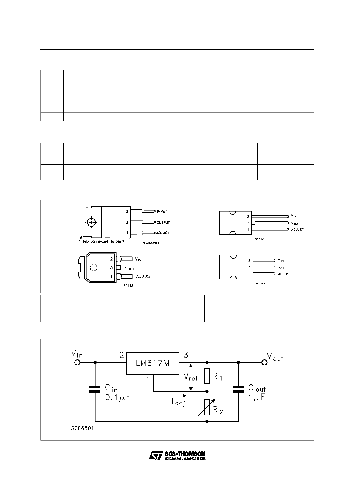
PINCONNECTION AND ORDERING NUMBERS
Input-Output Differential Voltage 40 V
i-Vo
P
Power Dissipation Internally Limited
d
Operating Junction Temperature Range (*) forLM217M
opr
forLM317M
T
StorageTemperature Range -55 to 150
stg
-40 to 125
0to125
TO-220 Unit
SOT-194
DPAK
ThermalResistance Junction-case Max
ThermalResistance Junction-ambient Max
8
100
TO-220 SOT-82
50
3
o
C/W
o
C/W
o
C
o
C
o
C
DPAK SOT-194
Type TO-220 DPAK SOT-82 SOT-194
LM217M LM217MT LM217 M DT LM217MX LM217 M S
LM317M LM317MT LM317 M DT LM317MX LM317 M S
TEST CIRCUIT
2/11
LM217M/LM317M
ELECTRICALCHARACTERISTICS FOR LM217M (Refer to the test circuits, -40 ≤ Tj≤ 125oC
V
(*) CADJ is connected between Adjust pinand Ground.
= 5 V, Io= 100 mA, Pd≤ 7.5W, unlessotherwisespecified)
i-Vo
Symbol Parameter Test Conditions Min. Typ. Max. Unit
LineRegulation Vi-Vo= 3 to40 V Tj=25oC 0.01 0.02 %/V
∆V
o
0.02 0.05 %/V
LoadRegulation Vo≤ 5V
∆V
o
I
Adjustment Pin Current 50 100 µA
ADJ
∆I
V
I
o(min)
I
o(max)
Adjustment Pin Current Vi-Vo= 3 to40 V
ADJ
Reference Voltage Vi-Vo= 3 to40 V
REF
∆
V
OutputVoltage Temperature
o
Stability
V
o
Minimum LoadCurrent Vi-Vo=40V 3.5 5 mA
Maximum OutputCurrent Vi-Vo≤15V
OutputNoise Voltage
e
N
(percentance of V
)
O
SVR Supply Voltage Rejection (*) T
=10mA to 500 mA
I
o
≥ 5V
V
o
=10mA to 500 mA
I
o
=10mA to 500 mA
I
o
=10mA to 500 mA
I
o
=40V, Pd<P
V
i-Vo
B = 10Hzto 10KHz
Tj=25oC
=25oC
j
f = 120Hz
T
T
dMAX,Tj
C
=25oC515mV
j
20 50 mV
=25oC 0.1 0.3 % /V
j
0.3 1 %/V
0.2 5 µ A
1.2 1.25 1.3 V
0.7 %
500 1000
=25oC
200
0.003 %
C
=0 65 dB
ADJ
=10µF66 80 dB
ADJ
o
o
mA
ELECTRICALCHARACTERISTICS FOR LM317M (Refer to the test circuits, 0 ≤ Tj≤ 125oC
V
= 5 V, Io= 100 mA, Pd≤ 7.5W, unlessotherwisespecified)
i-Vo
Symbol Parameter Test Conditions Min. Typ. Max. Unit
LineRegulation Vi-Vo= 3 to40 V Tj=25oC 0.01 0.04 %/V
∆V
o
0.02 0.07 %/V
LoadRegulation Vo≤ 5V
∆V
o
I
Adjustment Pin Current 50 100 µA
ADJ
∆I
V
I
o(min)
I
o(max)
Adjustment Pin Current Vi-Vo= 3 to40 V
ADJ
ReferenceVoltage Vi-Vo= 3 to40 V
REF
∆
V
OutputVoltage Temperature
o
Stability
V
o
Minimum Load Current Vi-Vo=40V 3.5 10 mA
Maximum OutputCurrent Vi-Vo≤15V
OutputNoise Voltage
e
N
(percentance of V
)
O
SVR Supply Voltage Rejection (*) T
=10mA to 500 mA
I
o
≥ 5V
V
o
=10mA to 500 mA
I
o
=10mA to 500 mA
I
o
=10mA to 500 mA
I
o
=40V, Pd<P
V
i-Vo
B = 10Hzto 10KHz
Tj=25oC
=25oC
j
f = 120Hz
T
T
dMAX,Tj
C
=25oC525mV
j
20 70 mV
=25oC 0.1 0.5 % /V
j
0.3 1. 5 %/ V
0.2 5 µ A
1.2 1.25 1.3 V
0.7 %
500 1000
=25oC
200
0.003 %
C
=0 65 dB
ADJ
=10µF66 80 dB
ADJ
o
o
mA
(*) CADJ is connected between Adjust pinand Ground.
3/11
LM217M/LM317M
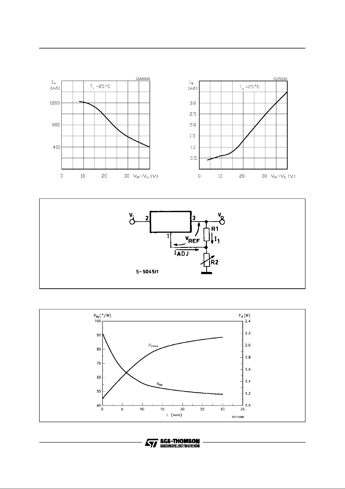
Figure1 : Current Limit Figure2 : MinimumOperatingCurrent
Figure3 : Basic AdjustableRegulator.
LM317M
Figure4 : ThermalResistance& MaximumPower Dissipationvs P.C.B. Copper Lenght for DPAK
Pdmax calculatedfor Ta=50oC
4/11
 Loading...