

现货库存、技术资料、百科信息、热点资讯,精彩尽在鼎好!
1.2 V to 37 V adjustable voltage regulators
Features
■ Output voltage range: 1.2 to 37 V
■ Output current in excess of 1.5 A
■ 0.1% Line and load regulation
■ Floating operation for high voltages
■ Complete series of protections: current limiting,
thermal shutdown and SOA control
Description
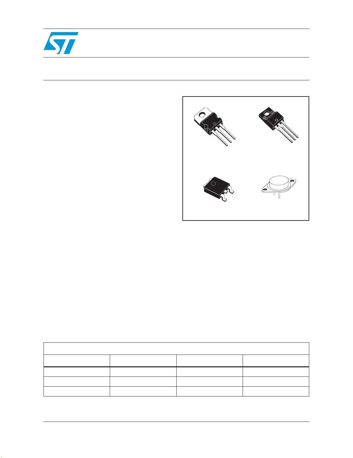
The LM117/LM217/LM317 are monolithic
integrated circuit in TO-220, TO-220FP, TO-3 and
2
D
PAK packages intended for use as positive
adjustable voltage regulators.
They are designed to supply more than 1.5 A of
load current with an output voltage adjustable
over a 1.2 to 37 V range.
LM117/LM217/LM317
TO-220
2
D
PAK
TO-220FP
TO-3
The nominal output voltage is selected by means
of only a resistive divider, making the device
exceptionally easy to use and eliminating the
stocking of many fixed regulators.
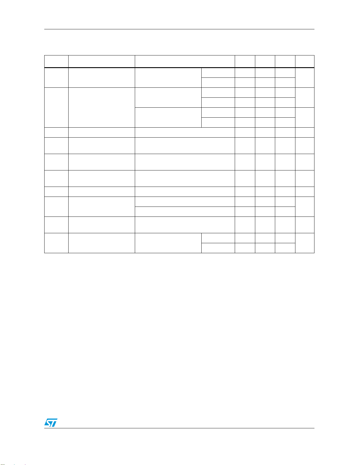
Table 1. Device summary
Order codes
TO-220 D
LM217T LM217D2T-TR LM217K
LM317T LM317D2T-TR LM317P LM317K
2
PAK (tape and reel) TO-220FP TO-3
LM117K
February 2008 Rev 14 1/25
www.st.com
25

Contents LM117/LM217/LM317
Contents
1 Pin configuration . . . . . . . . . . . . . . . . . . . . . . . . . . . . . . . . . . . . . . . . . . . 3
2 Maximum ratings . . . . . . . . . . . . . . . . . . . . . . . . . . . . . . . . . . . . . . . . . . . 4
3 Diagram . . . . . . . . . . . . . . . . . . . . . . . . . . . . . . . . . . . . . . . . . . . . . . . . . . . 5
4 Electrical characteristics . . . . . . . . . . . . . . . . . . . . . . . . . . . . . . . . . . . . . 6
5 Typical characteristics . . . . . . . . . . . . . . . . . . . . . . . . . . . . . . . . . . . . . . . 8
6 Application information . . . . . . . . . . . . . . . . . . . . . . . . . . . . . . . . . . . . . . 9
7 Package mechanical data . . . . . . . . . . . . . . . . . . . . . . . . . . . . . . . . . . . . 13
8 Revision history . . . . . . . . . . . . . . . . . . . . . . . . . . . . . . . . . . . . . . . . . . . 24
2/25
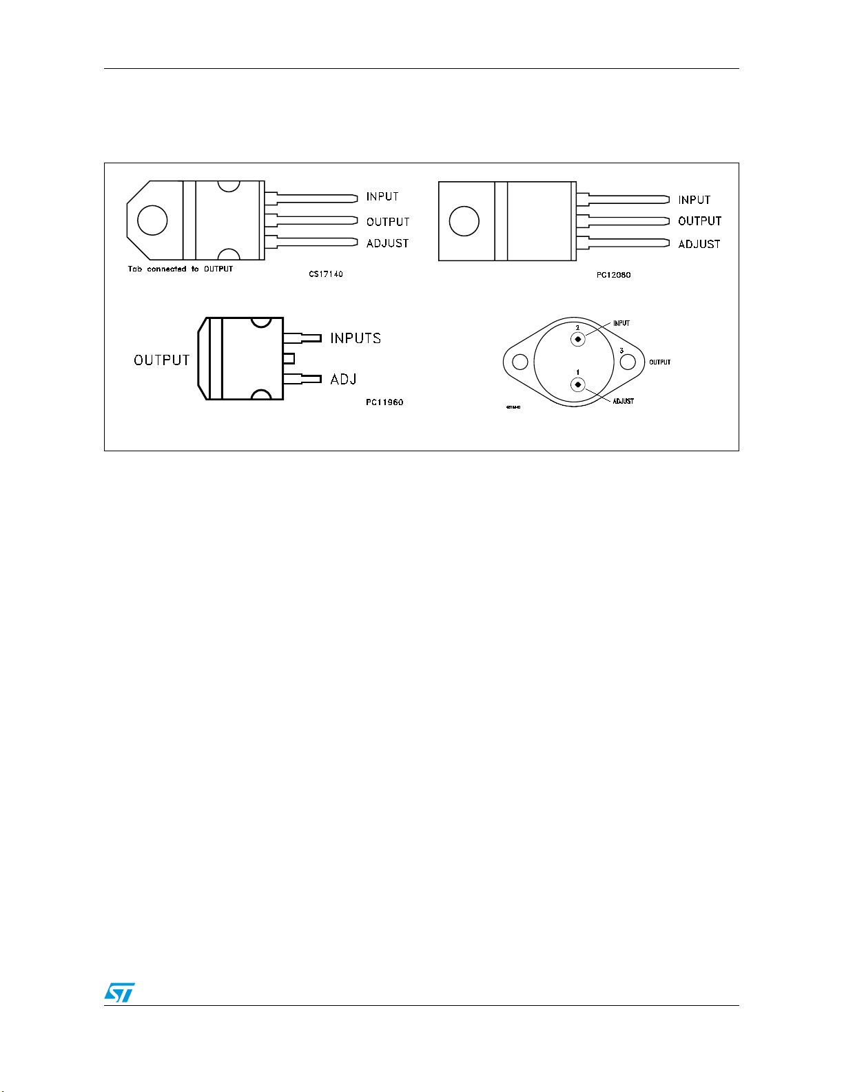
LM117/LM217/LM317 Pin configuration
1 Pin configuration
Figure 1. Pin connections (top view)
TO-220
D2PAK (Any Type)
TO-220FP
TO-3
3/25

Maximum ratings LM117/LM217/LM317
2 Maximum ratings
Table 2. Absolute maximum ratings
Symbol Parameter Value Unit
V
- VOInput-reference differential voltage 40
I
I
T
OP
Output current Internally limited
O
LM117 -55 to 150
Operating junction temperature for:
LM317 0 to 125
V
°CLM217 -25 to 150
T
P
STG
Power dissipation Internally limited
D
Storage temperature -65 to 150 °C
Note: Absolute maximum ratings are those values beyond which damage to the device may occur.
Functional operation under these condition is not implied.
Table 3. Thermal data
Symbol Parameter D2PAK TO-220 TO-220FP TO-3 Unit
R
R
Thermal resistance junction-case 3 3 5 4 °C/W
thJC
Thermal resistance junction-ambient 62.5 50 60 35 °C/W
thJA
4/25
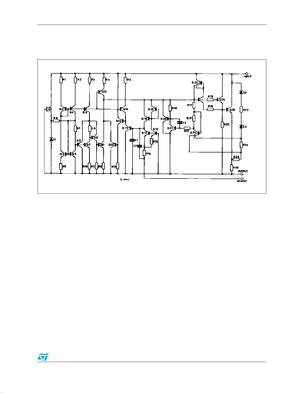
LM117/LM217/LM317 Diagram
3 Diagram
Figure 2. Schematic diagram
5/25
Electrical characteristics LM117/LM217/LM317
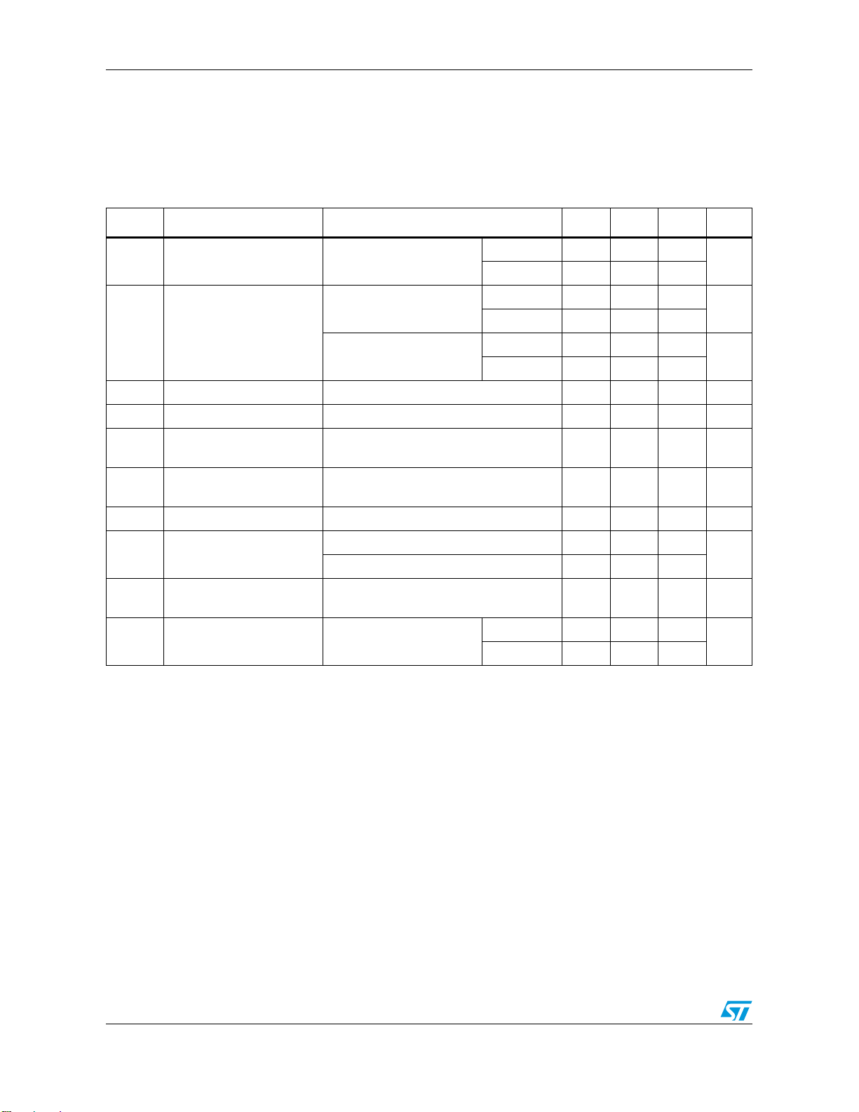
4 Electrical characteristics
Table 4. Electrical characteristics for LM117/LM217 (VI - VO = 5 V, IO = 500 mA, I
= 20 W, TJ = -55 to 150°C for LM117, TJ = -25 to 150 °C for LM217, unless otherwise
P
MAX
= 1.5 A and
MAX
specified)
Symbol Parameter Test conditions Min. Typ. Max. Unit
T
= 25°C 0.01 0.02
ΔV
ΔV
I
ΔI
V
ΔV
I
O(min)
I
O(max)
Line regulation VI - VO = 3 to 40 V
O
Load regulation
O
Adjustment pin current 50 100 µA
ADJ
Adjustment pin current VI - VO = 2.5 to 40V IO = 10 mA to I
ADJ
Reference voltage
REF
(between pin 3 and pin 1)
Output voltage
O/VO
temperature stability
Minimum load current VI - VO = 40 V 3.5 5 mA
Maximum load current
Output noise voltage
eN
(percentage of V
O
SVR Supply voltage rejection
1. C
is connected between pin 1 and ground.
ADJ
VO ≤5 V
IO = 10 mA to I
≥5 V,
V
O
= 10 mA to I
I
O
MAX
MAX
VI - VO = 2.5 to 40V IO= 10 mA to I
PD ≤ P
MAX
VI - VO ≤ 15 V, PD < P
- VO = 40 V, PD < P
V
I
)
B = 10Hz to 100kHz, T
(1)
TJ = 25°C, f = 120Hz
MAX
MAX
J
0.02 0.05
TJ = 25°C 5 15
20 50
TJ = 25°C 0.1 0.3
0.3 1
0.2 5 µA
MAX
MAX
1.2 1.25 1.3 V
1%
1.5 2.2
, TJ = 25°C 0.4
= 25°C 0.003 %
J
C
=0 65
ADJ
=10µF 66 80
C
ADJ
%/V
mV
%
A
dB
6/25
LM117/LM217/LM317 Electrical characteristics
Table 5. Electrical characteristics for LM317 (VI - VO = 5 V, IO = 500 mA, I
= 20 W, TJ = 0 to 125°C, unless otherwise specified)
P
MAX
= 1.5 A and
MAX
Symbol Parameter Test conditions Min. Typ. Max. Unit
T
= 25°C 0.01 0.04
ΔV
ΔV
I
ΔI
V
ΔV
I
O(min)
I
O(max)
Line regulation VI - VO = 3 to 40 V
O
Load regulation
O
Adjustment pin current 50 100 µA
ADJ
Adjustment pin current
ADJ
Reference voltage
REF
(between pin 3 and pin 1)
Output voltage
O/VO
temperature stability
Minimum load current VI - VO = 40 V 3.5 10 mA
Maximum load current
Output noise voltage
eN
(percentage of V
O
SVR Supply voltage rejection
1. C
is connected between pin 1 and ground.
ADJ
VO ≤ 5 V
IO = 10 mA to I
≥5 V,
V
O
= 10 mA to I
I
O
- VO = 2.5 to 40V,
V
I
= 10 mA to 500mA
I
O
MAX
MAX
VI - VO = 2.5 to 40V IO = 10 mA to 500mA
PD ≤ P
MAX
VI - VO ≤ 15 V, PD < P
- VO = 40 V, PD < P
V
I
)
B = 10Hz to 100kHz, T
(1)
TJ = 25°C, f = 120Hz
MAX
MAX
J
0.02 0.07
TJ = 25°C 5 25
20 70
TJ = 25°C 0.1 0.5
0.3 1.5
0.2 5 µA
1.21.251.3 V
1%
1.5 2.2
, TJ = 25°C 0.4
= 25°C 0.003 %
J
C
=0 65
ADJ
=10µF 66 80
C
ADJ
%/V
mV
%
A
dB
7/25

Typical characteristics LM117/LM217/LM317
5 Typical characteristics
Figure 3. Output current vs input-output
Figure 5. Reference voltage vs junction
differential voltage
Figure 4. Dropout voltage vs junction
temperature
Figure 6. Basic adjustable regulator
8/25
 Loading...