


ST LM101A, LM201A, LM301A User Manual

LM101A-LM201A
LM301A
SINGLE OPERATIONAL AMPLIFIERS
LM101A LM301A
LM201A
■ INPUT OFFSET VO LTAGE 0.7mV 2mV
■ INPUT BIAS CURRENT 25nA 70nA
■ INPUT OFFSET CURRENT 1.5nA 2nA
■ SLEW RATE AS INVERSING10V /µs 10V/µs
AMPLIFIER
DESCRIPTION
The LM101A is a general purpose operational amplifier which offers many features: supply voltages
from ±5V to ±22V, low current drai n, overload protection on the inpu t and outpu t, no latch-up when
the common-mode range is ex ceeded, free from
oscillations and compensation with a single 30pF
capacitor. It has advantages over internally compensated amplifiers in that t he compen sation can
be tailored to the particular application: slew rate
of 10V/µs and bandwidth of 3.5MHz can be easily
achieved.
ORDER CODE
Part Number Temperature Range
LM101A -55°C, +125°C
LM201A -40°C, +105°C
LM301A 0°C, +70°C
Example : LM201AN
N = Dual in Line Package (DIP)
D = Small Outline Package (SO) - also available in Tape & Reel (DT)
Package
ND
••
••
••
N
DIP8
(Plastic Package)
D
SO8
(Plastic Micropackage)
PIN CONNECTIONS (top view)
1
2
3
4
1 - Balance, compensation
2 - Inverting input
3 - Non-inverting input
-
4 - V
CC
5 - Balance
6 - Output
7 - V
8 - Compensation 2
CC
8
7
6
5
+
December 2001
1/11
LM101A - LM201A - LM301A
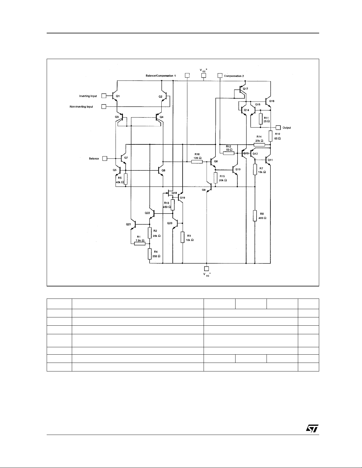
SCHEMATIC DIAGRAM
ABSOLUTE MAXIMUM RATINGS
Symbol Parameter LM101A LM201A LM301A Unit
V
P
T
T
2/11
Supply voltage ±22 V
CC
V
Input Voltage ±15 V
i
V
Differential Input Voltage ±30 V
id
Power Dissipation N Suffix
tot
D Suffix
500
300
Output Short-circuit Duration Infinite
Opearting Free-air Temperature Range -55 to +125 -40 to +105 0 to +70 °C
oper
Storage Temperature Range -65 to +150 °C
stg
mW

ELECTRICAL CHARACTERISTICS
±5V ≤ VCC ≤ ±20V, C1 = 30pF, T
Symbol Parameter
Input Offset Voltage (RS ≤ 10kΩ)
= +25°C
V
DV
io
T
amb
T
≤ T
min
amb
Input Offset Voltage Drift
io
≤ T
T
min
≤ T
amb
max
≤ T
Input Bias Current - note
I
ib
T
T
amb
min
= +25°C
≤ T
amb
≤ T
max
Input Offset Current
T
T
amb
min
= +25°C
≤ T
amb
≤ T
max
I
io
Input Offset Current Drift
T
≤ T
≤ T
amb
amb
≤ 25°C
≤ T
DI
Iio
min
T
min
Large Signal Voltage Gain *
10V, R
≤
V
A
vd
T
T
O
amb
min
= +25°C
≤ T
amb
= 2k
L
≤ T
max
Supply Voltage Rejection Ratio (R
T
T
amb
min
= +25°C
≤ T
amb
≤ T
max
SVR
Supply Current, no load
= +25°C
I
CC
T
T
amb
min
≤ T
amb
≤ T
max
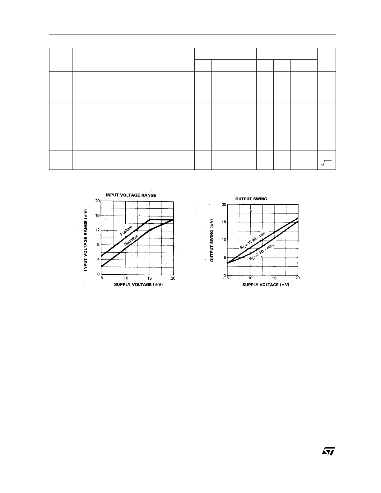
Input Common Mode Voltage Range
= ±20V)
(V
V
icm
CC
T
T
amb
min
≤ T
= +25°C
amb
≤ T
max
Common Mode Rejection Ratio (R
T
CMR
I
OS
= +25°C
amb
T
≤ T
amb
≤ T
max
min
Output Short-circuit Current *
= +25°C
T
amb
Output Voltage Swing *
= +25°C RL = 10k
T
amb
±V
OPP
SR
≤ T
T
min
Slew Rate (V
unity gain) -
≤ T
amb
max
= ±10V, RL = 2kΩ,CL = 100pF,
i
1)
= 25°C (unless otherwise specified)
amb
max
max
Ω)
≤ 10kΩ)
s
≤ 10kΩ)
s
= 2k
R
L
RL = 10k
R
= 2k
L
LM101A - LM201A - LM301A
LM101A - LM201A LM301A
Min. Typ. Max. Min. Typ. Max.
0.7 2
27.510mV
3
315 630
25 75
100
1.5 10
70 250
300
25070nA
20
10
20
100
200
10
20
300
600
5025100 2515100
808096 707096 dB
1.8 3
3
±15
±15
1.8 3
3
±15
±15
808096 707096 dB
10 30 50 10 30 50
Ω
Ω
Ω
Ω
12
10
12
10
14
13
12
14
10
13 V
12
10
0.25 0.5 0.25 0.5
Unit
V/°C
µ
nA
pA/°C
V/mV
mA
V
mA
V/µs
3/11
LM101A - LM201A - LM301A
Symbol Parameter
Rise (Vi = ±20mV, RL = 2kΩ,CL = 100pF, unity
t
r
gain)
Overshoot (Vi = 20mV, RL = 2kΩ,CL = 100pF,
K
OV
unity gain)
Z
Input Impedance * 1.5 4 1.5 4 M
i
Gain Bandwidth Product *
GBP
= 10mV, RL = 2kΩ,CL = 100pF, f = 100KHz)
(V
i
Total Harmonic Distortion
(f = 1kHz, A
THD
C
= 100pF)
L
Equivalent Input Noise Voltage
e
n
1. May be impr oved up to 10V/µs in i nverting ampli fier configuration
* ==> V
= ±15V, T
CC
f = 1kHz, R
= 20dB, RL = 2k
v
= 100
Ω
s
= +25°C (unle ss otherwise s pecified)
amb
Ω,
Vo = 2V
pp
,
LM101A - LM201A LM301A
Min. Typ. Max. Min. Typ. Max.
0.3 0.3
55
0.5 1 0.5 1
0.015 0.015
25 25
Unit
µs
%
Ω
MHz
%
nV
----------- Hz
4/11