

Features
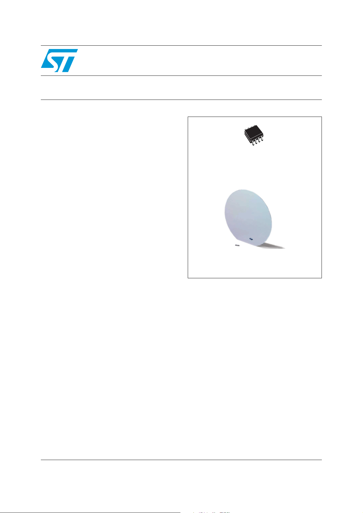
D
SO-8
(Plastic micropackage)
Wafer form
■ Internally frequency compensated
■ Large DC voltage gain: 100 dB
■ Wide bandwidth (unity gain: 1.1 MHz
temperature compensated)
■ Very low supply current per operator (500 µA)
■ Low input bias current: 20 nA
(temperaturecompensated)
■ Low input offset current: 2 nA
■ Input common-mode voltage range includes
ground
■ Differential input voltage range equal to the
power supply voltage
■ Large output voltage swing 0 V to V
■ Internal ESD protection:
–2kV HBM
–200V MM
CC
-1.5V
LM2904WH
Low power dual operational amplifier
Datasheet — production data
Description
also swing to ground, even though operated from
a single power supply.
This circuit consists of two independent, highgain, internally frequency-compensated operational
amplifiers, designed specifically for automotive
and industrial control systems. It operates from a
single power supply over a wide range of
voltages. The low power supply drain is
independent of the magnitude of the power supply
voltage.
Application areas include transducer amplifiers,
DC gain blocks and all the conventional op-amp
circuits which now can be more easily
implemented in single power supply systems. For
example, these circuits can be directly supplied
from standard +5 V which is used in logic systems
and will easily provide the required interface
electronics without requiring any additional power
supply.
In linear mode, the input common-mode voltage
range includes ground and the output voltage can
July 2012 Doc ID 9876 Rev 7 1/12
This is information on a product in full production.
www.st.com
12
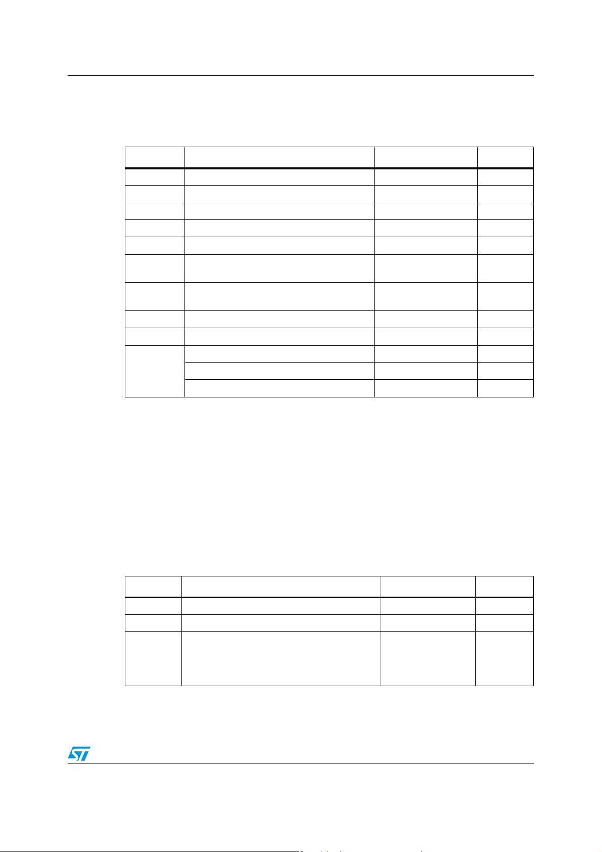
Schematic diagram LM2904WH
OUT 1OUT 2 Vcc +
E- (1)
E+ (1)
E- (2)
GNDE+ (2)
year
Die
id.
x
y
1021025555OUT2
10210270480Vcc +
10210255910OUT1
1021026201010E-1
1021021030940E+1
1021021040480GND
Pad dimensionsPad placementName
1021021030-30E+2
102102620-30E-2
YXYX
1021025555OUT2
10210270480Vcc +
10210255910OUT1
1021026201010E-1
1021021030940E+1
1021021040480GND
Pad dimensionsPad placementName
1021021030-30E+2
102102620-30E-2
YXYX
The origin coordinate is at the bottom left part of the
OUT2 pin. All dimensions are specified in micrometers (µm).
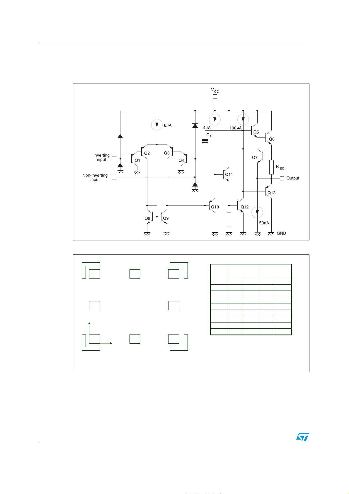
1 Schematic diagram
Figure 1. Schematic diagram (1/2 LM2904WH)
Figure 2. Pad locations
2/12 Doc ID 9876 Rev 7
LM2904WH Absolute maximum ratings and operating conditions
2 Absolute maximum ratings and operating conditions
Table 1. Absolute maximum ratings
Symbol Parameter Value Unit
+
V
CC
V
id
V
in
Supply voltage +32 V
Differential input voltage -0.3 to VCC+0.3 V
Input voltage -0.3 to VCC+0.3 V
Output short-circuit to ground
(1)
40 mA
T
j
R
thja
R
thjc
I
in
T
stg
ESD
1. Short-circuits from the output to V
current is approximately 40 mA, independent of the magnitude of V
from simultaneous short-circuits on all amplifiers.
2. Short-circuits can cause excessive heating and destructive dissipation. Values are typical.
3. This input current only exists when the voltage values applied on the inputs is beyond the supply voltage
line limits. This is not destructive if the current does not exceed 5 mA as indicated, and normal output is
restored for input voltages above -0.3V.
4. Human body model: A 100pF capacitor is charged to the specified voltage, then discharged through a
Ω resistor between two pins of the device. This is done for all couples of connected pin combinations
1.5k
while the other pins are floating.
5. Machine model: A 200pF capacitor is charged to the specified voltage, then discharged directly between
two pins of the device with no external series resistor (internal resistor < 5
connected pin combinations while the other pins are floating.
6. Charged device model: all pins and the package are charged together to the specified voltage and then
discharged directly to the ground through only one pin. This is done for all pins.
Maximum junction temperature 150 °C
Thermal resistance junction to ambient
SO-8
Thermal resistance junction to case
SO-8
Input current
(3)
(2)
125 °C/W
(2)
40 °C/W
5mA
Storage temperature range -65 to +150 °C
HBM: human body model
MM: machine model
CDM: charged device model
(4)
(5)
(6)
can cause excessive heating if V
CC
2kV
200 V
1.5 kV
+
> 15 V. The maximum output
CC
. Destructive dissipation can result
CC
Ω). This is done for all couples of
Table 2. Operating conditions
Symbol Parameter Value Unit
+
V
CC
T
oper
V
icm
1. The input common-mode voltage of either input signal voltage should not be allowed to go negative by
more than 0.3 V. The upper end of the common-mode voltage range is V
inputs can go to +32 V without damage.
Supply voltage 3 to 30 V
Operating free-air temperature range -40 to +150 °C
Input common mode voltage range
(V
CC
T
T
+
amb
min
=+30V)
= 25°C
≤ T
amb
(1)
≤ T
max
0 to V
0 to V
CC
+
-1.5
CC
+
-2
CC
+
–1.5 V, but either or both
Doc ID 9876 Rev 7 3/12
V
Electrical characteristics LM2904WH
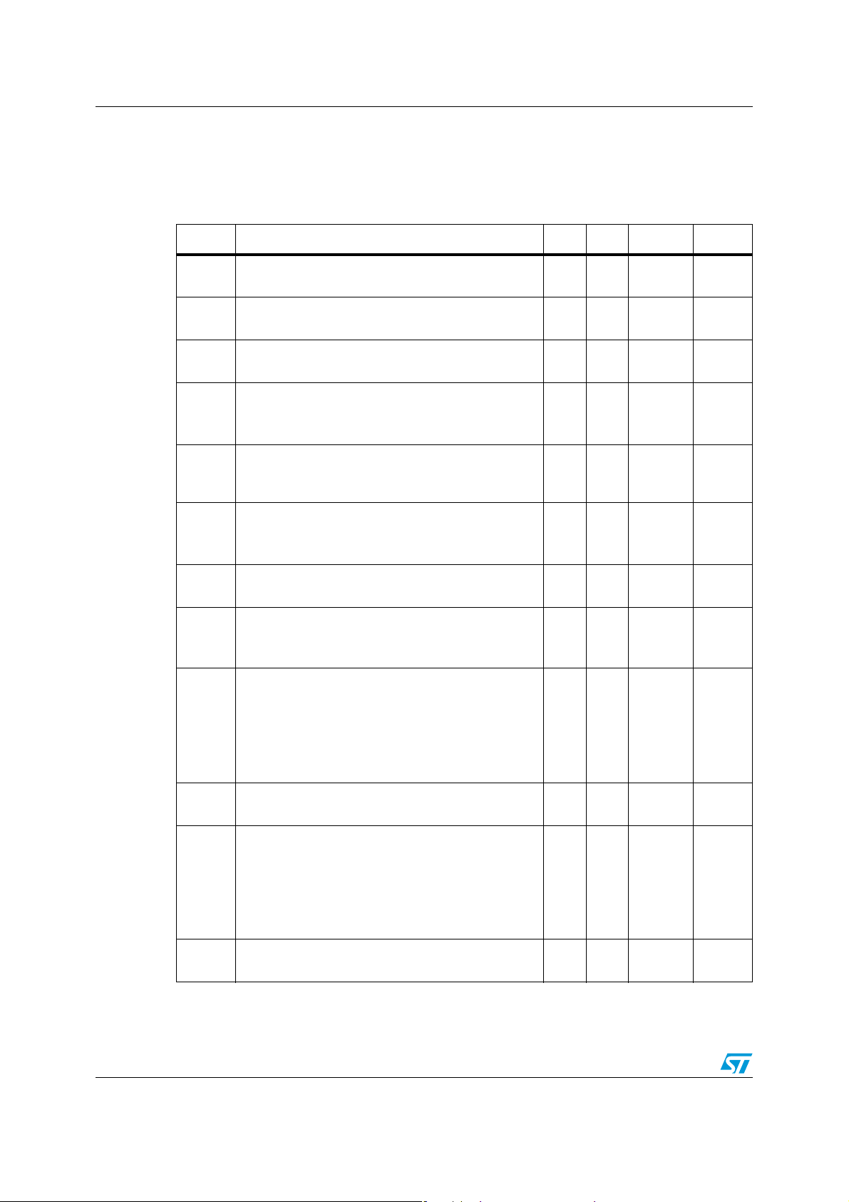
3 Electrical characteristics
Table 3 . V
CC
+
= 5V, V
-
= Ground, Vo = 1.4V, T
CC
= 25°C (unless otherwise
amb
specified)
Symbol Parameter Min. Typ. Max. Unit
V
I
io
I
ib
A
SVR
I
CC
CMR
I
source
I
sink
V
OPP
V
OH
V
OL
Input offset voltage
io
T
≤ T
min
amb
Input offset current
T
≤ T
min
amb
Input bias current
T
≤ T
min
amb
Large signal voltage gain
+
V
vd
= +15V,RL=2kΩ, Vo = 1.4V to 11.4V
CC
T
≤ T
min
amb
Supply voltage rejection ratio
+
= +5 to +30V, RS ≤ 10kΩ
V
CC
T
≤ T
min
amb
Supply current, all amps, no load
+
V
= +5V
CC
T
≤ T
min
amb
Common-mode rejection ratio (R
T
≤ T
min
amb
Output short-circuit current
+
V
= +15V, Vo = +2V, Vid = +1V
CC
T
≤ T
min
amb
Output sink current
V
= 2V, V
O
T
≤ T
min
amb
VO = +0.2V, V
T
≤ T
min
amb
Output voltage swing (RL = 2kΩ)
T
≤ T
min
amb
High level output voltage (V
RL = 2kΩ
T
≤ T
min
amb
RL = 10kΩ
T
≤ T
min
amb
Low level output voltage (RL = 10kΩ)
T
≤ T
min
amb
≤ T
≤ T
≤ T
≤ T
≤ T
≤ T
≤ T
≤ T
CC
≤ T
≤ T
≤ T
≤ T
≤ T
≤ T
(1)
max
max
(2)
max
max
max
, VCC = +30V
max
max
max
+
= +5V
max
+
= +15V
CC
max
max
max
max
max
27
9
230
40
20 150
200
50
100 V/mV
2.5
6565100
0.7 1.2
2
= 10kΩ)
S
706085
201040 60 mA
10
20
5
12
50
10
+
V
-1.5
CC
+
V
-2
CC
+
= + 30V)
CC
26
0
0
27
26
27
28
27
520
20
mV
nA
nA
dB
mA
dB
mA
µA
V
V
mV
4/12 Doc ID 9876 Rev 7

LM2904WH Electrical characteristics
Table 3 . V
CC
+
= 5V, V
-
= Ground, Vo = 1.4V, T
CC
= 25°C (unless otherwise
amb
specified) (continued)
Symbol Parameter Min. Typ. Max. Unit
Slew rate (unity gain)
SR
GBP
THD
e
n
DV
io
DI
io
V
O1/VO2
1. VO = 1.4 V, RS = 0 Ω, 5 V < V
2. The direction of the input current is out of the IC. This current is essentially constant, independent of the
state of the output, so there is no change in the loading charge on the input lines.
3. Due to the proximity of external components, ensure that stray capacitance does not cause coupling
between these external parts. Typically, this can be detected because this type of capacitance increases at
higher frequencies.
+
V
= 15V, Vi = 0.5 to 3V, RL = 2kΩ, CL = 100pF,
CC
T
≤ T
amb
≤ T
max
min
0.3
0.6 V/µs
0.2
Gain bandwidth product f = 100kHz
+
V
= 30V, Vin = 10mV, RL = 2kΩ, CL = 100pF
CC
T
≤ T
amb
≤ T
max
min
0.7
0.45
1.1 MHz
Total harmonic distortion
f = 1kHz, A
C
= 100pF, VCC = 30V
L
Equivalent input noise voltage
f=1kHz, RS=100Ω, VCC=30V
= 20dB, RL = 2kΩ, Vo = 2Vpp,
V
0.02
55
nV/
Input offset voltage drift 7 30 µV/°C
Input offset current drift 10 300 pA/°C
Channel separation
(3)
1kHz ≤ f ≤ 20kHz 120
+
< 30 V, 0 V < Vic < V
CC
CC
+
- 1.5 V.
%
√Hz
dB
Doc ID 9876 Rev 7 5/12

Electrical characteristics LM2904WH
10
0
10
1
10
2
10
3
10
4
10
5
10
6
0
20
40
60
80
100
120
T
Ambient
=+150°C
T
Ambient
=+125°C
T
Ambient
=+25°C
GAIN (dB)
FREQUENCY (Hz)
FREQUENCY (Hz)
1k 10k 100k 1M
OUTPUT SWING (Vpp)
+7V
2k
Ω
1k
Ω
100k
Ω
+15V
VO
-
+
V
I
20
15
10
5
0
INPUT
VOLTAGE (V)
OUTPUT
VOLTAGE (V)
010203040
T
I
M
E
(
μ
s
)
RL 2 k
Ω
VCC = +15V
4
3
2
1
0
3
2
1
10 20 30
0
10
20
30
40
50
T
Ambient
=-40°C
T
Ambient
=+25°C
T
Ambient
=+125°C
T
Ambient
=+150°C
INPUT BIAS CURRENT (nA)
SUPPLY VOLTAGE (V)
OUTPUT VOLTAGE REFERENCED
TO V
CC
+
(V)
0,01 0,1 1 10 100
0,001
Independent of V
CC
T
amb
= +25°C
+
-
V
CC
V
O
I
O
VCC/2
OUTPUT SOURCE CURRENT (mA)
8
7
6
5
4
3
2
1
Figure 3. Open loop frequency response Figure 4. Large signal frequency response
Figure 5. Voltage follower pulse response Figure 6. Input bias current
Figure 7. Supply current Figure 8. Output characteristics
1.5
1.0
0.5
SUPPLY CURRENT (mA)
0.0
6/12 Doc ID 9876 Rev 7
Ambient
0102030
=-40°C
T
Ambient
T
=+125°C
Ambient
T
Ambient
SUPPLY VOLTAGE (V)
=+25°CT
=+150°C

LM2904WH Electrical characteristics
OUTPUT SINK CURRENT (μ A)
0,001 0,01 0,1 1 10 100
OUTPUT VOLTAGE (V)
VCC = +5V
VCC = +15V
VCC = +30V
-
I
O
V
O
T
amb
=+25°C
vcc/2
v
cc
+
10
1
0.1
0.01
OUTPUT CURRENT (mA)
-
+
I
O
TEMPERATURE (°C)
90
80
70
60
50
40
30
20
10
0
-55 -35 -15 5 25 45 65 85 105 125
OUTPUT VOLTAGE (mV)
0 1 2 3 4 5 6 7 8
Input
T
amb
= +25°C
VCC= 30 V
Output
e
O
e
l
50pF
+
-
TIME (ms)
500
450
400
350
300
250
INPUT VOLTAGE (V)
051015
POWER SUPPLY VOLTAGE (±V)
Négative
Positive
15
10
5
010203040
POSITIVE SUPPLY VOLTAGE (V)
VOLTAGE GAIN (dB)
160
120
80
40
L
R = 20k
Ω
L
R=2k
Ω
-55-35-15 5 25 45 65 85 105 125
TEMPERATURE (°C)
GAIN BANDWIDTH PRODUCT (MHz)
CC
V = 15V
1.5
1.35
1.2
1.05
0.9
0.75
0.6
0.45
0.3
0.15
0
Figure 9. Output characteristics Figure 10. Current limiting
Figure 11. Voltage follower pulse response Figure 12. Input voltage range
Figure 13. Voltage gain Figure 14. Gain bandwidth product
Doc ID 9876 Rev 7 7/12

Electrical characteristics LM2904WH
-55-35-15 5 25 45 65 85 105 125
TEMPERATURE (°C)
POWER SUPPLY REJECTION RATIO (dB)
SVR
115
110
105
100
95
90
85
80
75
70
65
60
-55-35-15 5 25 45 65 85 105 125
TEMPERATURE (°C)
COMMON MODE REJECTION RATIO (dB)
115
110
105
100
95
90
85
80
75
70
65
60
Figure 15. Power supply rejection ratio versus
temperature
Figure 16. Common mode rejection ratio
versus temperature
8/12 Doc ID 9876 Rev 7

LM2904WH Package information
4 Package information
In order to meet environmental requirements, ST offers these devices in different grades of
ECOPACK® packages, depending on their level of environmental compliance. ECOPACK®
specifications, grade definitions and product status are available at: www.st.com
is an ST trademark.
. ECOPACK
Doc ID 9876 Rev 7 9/12

Package information LM2904WH
Figure 17. SO-8 package mechanical drawing
Table 4. SO-8 package mechanical data
Dimensions
Ref.
Millimeters Inches
Min. Typ. Max. Min. Typ. Max.
A 1.75 0.069
A1 0.10 0.25 0.004 0.010
A2 1.25 0.049
b 0.28 0.48 0.011 0.019
c 0.17 0.23 0.007 0.010
D 4.80 4.90 5.00 0.189 0.193 0.197
E 5.80 6.00 6.20 0.228 0.236 0.244
E1 3.80 3.90 4.00 0.150 0.154 0.157
e 1.27 0.050
h 0.25 0.50 0.010 0.020
L 0.40 1.27 0.016 0.050
k1°8°1°8°
ccc 0.10 0.004
10/12 Doc ID 9876 Rev 7

LM2904WH Ordering information
5 Ordering information
Table 5. Order codes
Order code
Temperature
JLM2904WH-CD1
LM2904WHD
LM2904WHDT
LM2904WHYDT
1. Qualified and characterized according to AEC Q100 and Q003 or equivalent, advanced screening
according to AEC Q001 & Q 002 or equivalent.
(1)
-40°C, +150°C
6 Revision history
Table 6. Document revision history
Date Revision Changes
01-Sep-2003 1 Initial release.
01-Jul-2005 2
01-Oct-2005 3
range
Package Packing Marking
Wafer
SO-8
SO-8
(Automotive grade)
Tu b e o r
Tape & reel
Tu b e o r
Tape & reel
2904WH
2904WHY
PPAP references inserted in the datasheet, see Section 5: Ordering
information.
Correction of error in A
min. value in Ta b le 3 .
VD
Minor grammatical and formatting changes throughout.
27-Sep- 2006 4 Correction of error in A
ESD values added in Table 1: Absolute maximum ratings.
20-Jul-2007 5
Equivalent input noise parameter added in Ta b le 3 .
Electrical characteristics curves updated.
Section 4: Package information updated.
Added R
thja
and R
thjc
ratings.
07-Apr-2008 6
Updated format of package information for SO-8.
Corrected marking error in Table 5: Order codes (2904WHY, not
2904WY).
04-Jul-2012 7
Removed commercial type LM2904WHYD.
Updated Table 5: Order codes.
Doc ID 9876 Rev 7 11/12
min. value in Ta b le 3 .
VD
parameters in Table 1: Absolute maximum

LM2904WH
Please Read Carefully:
Information in this document is provided solely in connection with ST products. STMicroelectronics NV and its subsidiaries (“ST”) reserve the
right to make changes, corrections, modifications or improvements, to this document, and the products and services described herein at any
time, without notice.
All ST products are sold pursuant to ST’s terms and conditions of sale.
Purchasers are solely responsible for the choice, selection and use of the ST products and services described herein, and ST assumes no
liability whatsoever relating to the choice, selection or use of the ST products and services described herein.
No license, express or implied, by estoppel or otherwise, to any intellectual property rights is granted under this document. If any part of this
document refers to any third party products or services it shall not be deemed a license grant by ST for the use of such third party products
or services, or any intellectual property contained therein or considered as a warranty covering the use in any manner whatsoever of such
third party products or services or any intellectual property contained therein.
UNLESS OTHERWISE SET FORTH IN ST’S TERMS AND CONDITIONS OF SALE ST DISCLAIMS ANY EXPRESS OR IMPLIED
WARRANTY WITH RESPECT TO THE USE AND/OR SALE OF ST PRODUCTS INCLUDING WITHOUT LIMITATION IMPLIED
WARRANTIES OF MERCHANTABILITY, FITNESS FOR A PARTICULAR PURPOSE (AND THEIR EQUIVALENTS UNDER THE LAWS
OF ANY JURISDICTION), OR INFRINGEMENT OF ANY PATENT, COPYRIGHT OR OTHER INTELLECTUAL PROPERTY RIGHT.
UNLESS EXPRESSLY APPROVED IN WRITING BY TWO AUTHORIZED ST REPRESENTATIVES, ST PRODUCTS ARE NOT
RECOMMENDED, AUTHORIZED OR WARRANTED FOR USE IN MILITARY, AIR CRAFT, SPACE, LIFE SAVING, OR LIFE SUSTAINING
APPLICATIONS, NOR IN PRODUCTS OR SYSTEMS WHERE FAILURE OR MALFUNCTION MAY RESULT IN PERSONAL INJURY,
DEATH, OR SEVERE PROPERTY OR ENVIRONMENTAL DAMAGE. ST PRODUCTS WHICH ARE NOT SPECIFIED AS "AUTOMOTIVE
GRADE" MAY ONLY BE USED IN AUTOMOTIVE APPLICATIONS AT USER’S OWN RISK.
Resale of ST products with provisions different from the statements and/or technical features set forth in this document shall immediately void
any warranty granted by ST for the ST product or service described herein and shall not create or extend in any manner whatsoever, any
liability of ST.
ST and the ST logo are trademarks or registered trademarks of ST in various countries.
Information in this document supersedes and replaces all information previously supplied.
The ST logo is a registered trademark of STMicroelectronics. All other names are the property of their respective owners.
© 2012 STMicroelectronics - All rights reserved
STMicroelectronics group of companies
Australia - Belgium - Brazil - Canada - China - Czech Republic - Finland - France - Germany - Hong Kong - India - Israel - Italy - Japan -
Malaysia - Malta - Morocco - Philippines - Singapore - Spain - Sweden - Switzerland - United Kingdom - United States of America
www.st.com
12/12 Doc ID 9876 Rev 7
 Loading...