

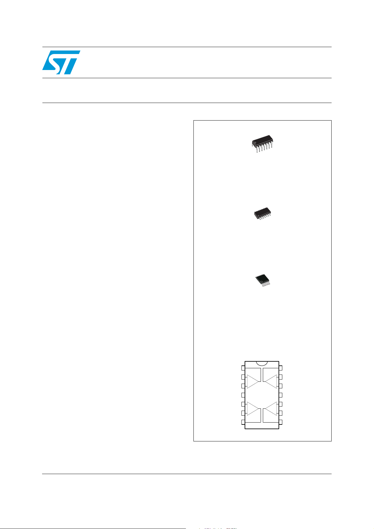
Low-power quad operational amplifier
Features
■ Wide gain bandwidth: 1.3 MHz
■ Input common-mode voltage range includes
negative rail
■ Large voltage gain: 100 dB
■ Very low supply current per amplifier: 375 µA
■ Low input bias current: 20 nA
■ Low input offset current: 2 nA
■ ESD internal protection: 800 V
■ Wide power supply range
■ Single supply: +3 V to +30 V
■ Dual supplies: ±1.5 V to ±15 V
Description
LM2902W
N
DIP14
(Plastic package)
D
SO-14
(Plastic micropackage)
This circuit consists of four independent, highgain, internally frequency-compensated
operational amplifiers designed especially for
automotive and industrial control systems.
The device operates from a single power supply
over a wide range of voltages. Operation from
split power supplies is also possible and the low
power supply current drain is independent of the
magnitude of the power supply voltage.
All the pins are protected against electrostatic
discharges up to 800 V.
(Thin shrink small outline package)
Output 1
Inverting Input 1
Non-inverting Input 1
Non-inverting Input 2
Inverting Input 2
Output 2
P
TSSOP14
Pin connections (top view)
Output 4
14
Inverting Input 4
13
Non-inverting Input 4
12
V
11
CC
10
Non-inverting Input 3
9
Inverting Input 3
8
Output 3
V
CC
1
2
-
+
3
+
4
5
+
-
6
7
-
+
+
-
-
February 2012 Doc ID 9922 Rev 8 1/17
www.st.com
17
Absolute maximum ratings and operating conditions LM2902W
1 Absolute maximum ratings and operating conditions
Table 1. Absolute maximum ratings
Symbol Parameter Value Unit
V
V
V
I
T
R
R
ESD
1. Short-circuits from the output to V
maximum output current is approximately 20 mA, independent of the magnitude of V
2. This input current only exists when the voltage at any of the input leads is driven negative. It is due to the
collector-base junction of the input PNP transistor becoming forward biased and thereby acting as input
diode clamps. In addition to this diode action, there is also NPN parasitic action on the IC chip. This
transistor action can cause the output voltages of the op-amps to go to the V
for a large overdrive) for the time during which an input is driven negative. This is not destructive and
normal output is restored for input voltages higher than -0.3 V.
3. R
thja/c
4. Human body model: a 100 pF capacitor is charged to the specified voltage, then discharged through a
1.5kΩ resistor between two pins of the device. This is done for all couples of connected pin combinations
while the other pins are floating.
5. Machine model: a 200 pF capacitor is charged to the specified voltage, then discharged directly between
two pins of the device with no external series resistor (internal resistor < 5Ω). This is done for all couples of
connected pin combinations while the other pins are floating.
6. Charged device model: all pins and the package are charged together to the specified voltage and then
discharged directly to the ground through only one pin. This is done for all pins.
Table 2. Operating conditions
Supply voltage ±16 to 32 V
CC
Differential input voltage +32 V
id
Input voltage -0.3 to V
i
Output short-circuit to ground
Input current
in
Storage temperature range -65 to +150 °C
stg
(2)
Thermal resistance junction to ambient
thja
SO-14
TSSOP14
(1)
(3)
DIP14
Thermal resistance junction to case
thjc
SO-14
TSSOP14
(3)
DIP14
HBM: human body model
MM: machine model
CDM: charged device model
are typical values.
(4)
(5)
(6)
+
can cause excessive heating and potential destruction. The
CC
+
+ 0.3 V
CC
Infinite
50 mA
105
100
80
31
32
33
800 V
100 V
1500 V
CC
voltage level (or to ground
CC
°C/W
°C/W
+
Symbol Parameter Value Unit
V
V
T
oper
Supply voltage 3 to 30 V
CC
Common mode input voltage range
icm
≤ T
T
min
amb
≤ T
max
Operating free-air temperature range -40 to +125 °C
2/17 Doc ID 9922 Rev 8
-
V
CC
V
CC
to V
-
to V
CC
CC
+
- 1.5
+
- 2
V
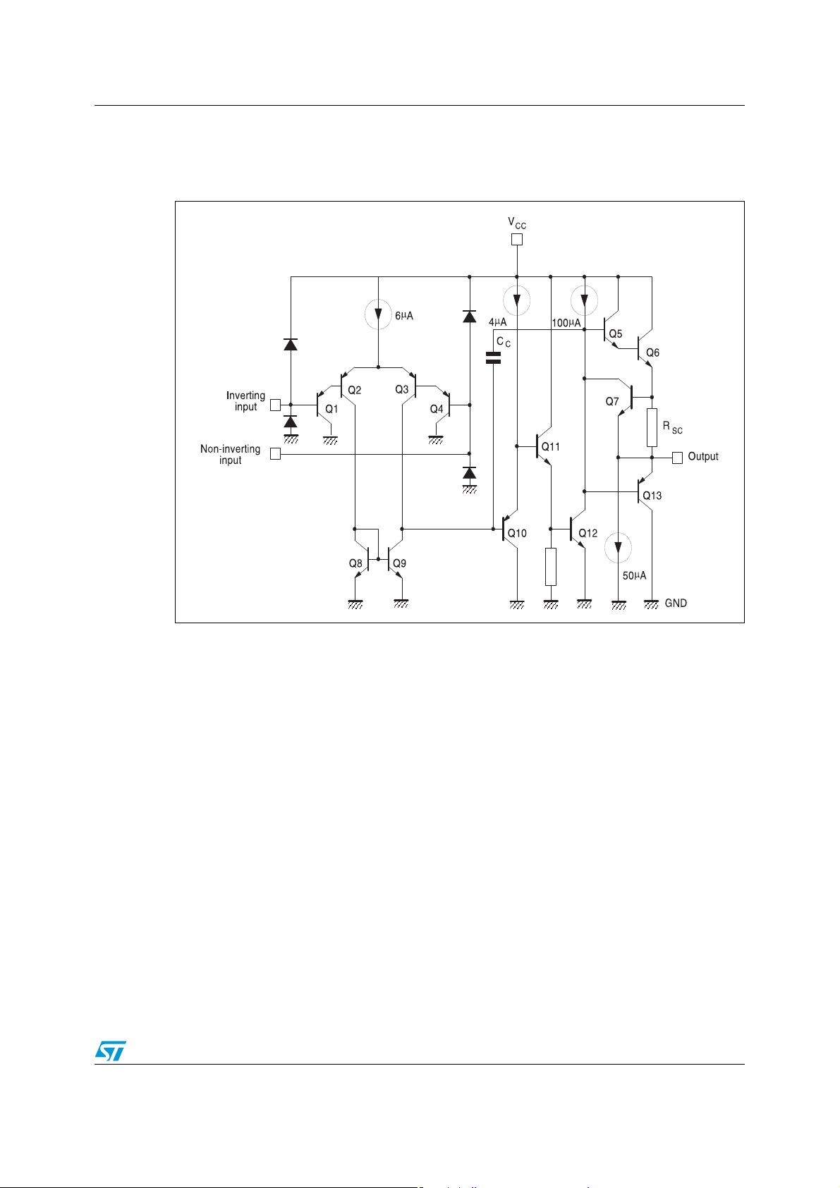
LM2902W Circuit schematics
2 Circuit schematics
Figure 1. Schematic diagram (1/4 LM2902)
Doc ID 9922 Rev 8 3/17
Electrical characteristics LM2902W
3 Electrical characteristics
Table 3. V
CC
+
=5V, V
(unless otherwise stated)
Symbol Parameter Test conditions Min. Typ. Max. Unit
-
= ground, VO= 1.4 V, T
CC
amb
= 25° C
V
DV
DI
A
Input offset voltage
i o
Input offset voltage drift 7 30 µV/°C
io
I
Input offset current
io
Input offset current drift 10 200 pA/°C
io
I
Input bias current
ib
Large signal voltage gain
vd
(1)
(2)
SVR Supply voltage rejection ratio
Supply current
I
CC
(all op-amps, no load)
CMR Common-mode rejection ratio
Output short-circuit current Vid = +1V, VCC+ = +15V, Vo = +2V 20 40 70 mA
I
o
I
V
Output sink current
sink
High level output voltage
OH
LM2902W
LM2902AW
≤ T
≤ T
T
min
T
T
T
T
T
V
amb
≤ T
min
amb
= +25°C 2 30
amb
≤ T
min
amb
= +25°C 20 150
amb
≤ T
min
amb
+
= +15V, RL=2kΩ,
CC
Vo= 1.4V to 11.4V, T
+
= +15V, RL=2kΩ,
V
CC
= 1.4V to 11.4V,
V
o
T
≤ T
min
amb
R
≤ 10kΩ, T
S
≤ 10kΩ, T
R
S
T
= +25°C, VCC+ = +5V 0.7 1.2
amb
T
= +25°C, VCC+ = +30V 1.5 3
amb
T
≤ T
min
amb
≤ T
T
min
amb
R
≤ 10kΩ, T
S
≤ 10kΩ, T
R
S
V
= -1V, VCC+ = +15V, Vo = +2V 10 20 mA
id
V
= -1V, VCC+ = +15V, Vo = +0.2V 12 50 µA
id
+ = 30V, RL = 2kΩ:
V
CC
T
= +25°C
amb
≤ T
T
min
amb
+ = 30V, RL = 10kΩ:
V
CC
= +25°C,
T
amb
T
≤ T
min
amb
V
+ = 5V, RL = 2kΩ:
CC
T
= +25°C
amb
T
≤ T
min
amb
LM2902W
max
≤ T
≤ T
≤ T
LM2902AW
max
max
max
amb
= + 25°C
50 100
25
≤ T
max
=+ 25°C 65 110
amb
≤ T
min
≤ T
≤ T
amb
min
max
max, VCC
≤ T
≤ T
amb
max
, VCC+ = +5V 0.9 1.2
+ = +30V 1.5 3
= +25°C 70 80
≤ T
amb
max
65
60
26
≤ T
max
26
27
≤ T
max
27
3.5
≤ T
max
3
27
2
9
4
40
300
27
28
mV
nA
nA
V/mV
dB
mA
dB
V
4/17 Doc ID 9922 Rev 8
LM2902W Electrical characteristics
Table 3. V
CC
+
=5V, V
-
= ground, VO= 1.4 V, T
CC
amb
= 25° C
(unless otherwise stated) (continued)
Symbol Parameter Test conditions Min. Typ. Max. Unit
R
= 10kΩ, T
V
Low level output voltage
OL
SR Slew rate
GBP Gain bandwidth product
THD Total harmonic distortion
Equivalent input noise voltage f = 1kHz, RS= 100Ω, VCC+ = 30V 40
e
n
V
O1/VO2
1. VO = 1.4 V, RS = 0 Ω, 5 V < V
2. The direction of the input current is out of the IC. This current is essentially constant, independent of the state of the output,
3. Due to the proximity of external components ensure that stray capacitance does not cause coupling between these
Channel separation
so there is no change in the load on the input lines.
external parts. This typically can be detected as this type of capacitance increases at higher frequencies.
(3)
+
< 30 V, 0 V < Vic < V
CC
L
= 10kΩ, T
R
L
+ = 15V, Vin= 0.5 to 3V,
V
CC
= 2kΩ, CL= 100pF, unity gain
R
L
< Top < T
T
min
+ = 30V, Vin= 10mV, RL= 2kΩ,
V
CC
CL= 100pF
f=1kHz, A
Vo=2Vpp, CL= 100pF, VCC+= 30V
1kHz ≤ f ≤ 20kHz 120 dB
CC
= +25°C 5 20
amb
≤ T
amb
≤ T
max
min
0.24
max
= 20dB, RL=2kΩ,
V
+
- 1.5 V.
0.14
20
mV
0.4 V/µs
1.3 MHz
0.015 %
nV/
√Hz
Doc ID 9922 Rev 8 5/17
Electrical characteristics LM2902W
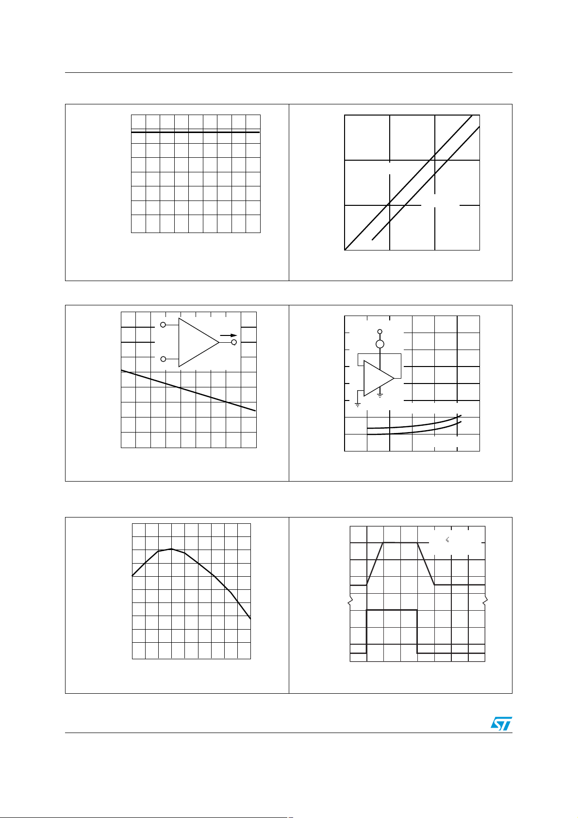
24
amb
Figure 3. Input voltage range
15
Figure 2. Input bias current vs. T
IB (nA)
21
18
15
12
10
Négative
9
6
3
5
INPUT VOLTAGE (V)
0
-55-35-15 5 25 45 65 85 105 125
AMBIENT TEMPERATURE (°C)
051015
POWER SUPPLY VOLTAGE (±V)
Figure 4. Current limiting Figure 5. Supply current
90
80
70
60
50
40
30
20
OUTPUT CURRENT (mA)
10
0
-55 -35 -15 5 25 45 65 85 105 125
-
+
I
TEMPERATURE (°C)
O
4
V
CC
I
D
3
2
1
mA
-
+
T
amb
SUPPLY CURRENT (mA)
0102030
POSITIVE SUPPLY VOLTAGE (V)
Positive
= 0°C to +125°C
T
= -55°C
amb
Figure 6. Gain bandwidth product Figure 7. Voltage follower pulse response
(V
= 15 V)
CC
GBP (mhz)
1.35
1.30
1.25
1.2
OUTPUT
1.15
1.1
1.05
1
-95
-9
-55-35-15 5 25 45 65 85 105 125
AMBIENT TEMPERATURE (°C)
GAIN BANDWIDTH PRODUCT (MHz)
6/17 Doc ID 9922 Rev 8
INPUT
4
(
E
RL 2 k
VCC = +15V
μ
)
s
3
2
1
VOLTAGE (V)
0
3
2
1
010203040
VOLTAGE (V)
M
T
I
Ω

LM2902W Electrical characteristics
0
Figure 8. Common-mode rejection ratio Figure 9. Output characteristics (sink)
COMMON MODE REJECTION RATIO (dB)
120
100
80
60
40
20
0
100 1K
+7.5V
Ω
100
-
Ω
100
e
I
100k
+
Ω
+7.5V
10K 100K
FREQUENCY (Hz)
100k
Ω
e
O
1M
10
VCC = +5V
VCC = +15V
VCC = +30V
1
vcc/2
v
-
0.1
T
+
amb
OUTPUT VOLTAGE (V)
0.01
0,001 0,01 0,1 1 10 10
OUTPUT SINK CURRENT (mA)
cc
= +25°C
I
O
V
O
Figure 10. Open-loop frequency response Figure 11. Voltage follower pulse response
(V
= 30 V)
CC
140
120
100
0.1μF
V
I
VCC/2
80
VCC= 30V &
60
-55°C
40
VOLTAGE GAIN (dB)
20
VCC= +10 to + 15V &
T
amb
+125°C
-55°C
0
1.0 10 100 1k 10k 100k 1M 10M
FREQUENCY (Hz)
T
-
+
amb
10M
Ω
V
CC
+125°C
V
O
500
450
+
e
-
l
e
50pF
O
400
Input
350
Output
300
OUTPUT VOLTAGE (mV)
250
012345678
T
=+25°C
amb
VCC=30V
TIME (μs)
Figure 12. Large signal frequency response Figure 13. Output characteristics (source)
20
Ω
1k
-
15
V
I
+
+7V
10
5
OUTPUT SWING (Vpp)
0
1k 10k 100k 1M
FREQUENCY (Hz)
100k
Ω
+15V
2k
VO
Ω
Doc ID 9922 Rev 8 7/17
8
V
CC
7
VCC/2
6
(V)
5
+
CC
4
TO V
3
2
OUTPUT VOLTAGE REFERENCED
1
0,001
+
-
Independent of V
T
amb
0,01 0,1 1 10 100
CC
= +25°C
OUTPUT SOURCE CURRENT (mA)
V
O
I
O

Electrical characteristics LM2902W
Figure 14. Input current Figure 15. Voltage gain
100
75
50
25
INPUT CURRENT (nA)
0 10 20 30
POSITIVE SUPPLY VOLTAGE (V)
T = +25°C
amb
Figure 16. Power supply and common-mode
Figure 17. Large signal voltage gain
160
120
80
40
VOLTAGE GAIN (dB)
0102030
POSITIVE SUPPLY VOLTAGE (V)
rejection ratio
120
115
R = 20k
L
R=2k
L
Ω
Ω
110
105
100
-55-35-15 5 25 45 65 85 105 125
LARGE SIGNAL VOLTAGE GAIN
AMBIENT TEMPERATURE (°C)
-55
8/17 Doc ID 9922 Rev 8
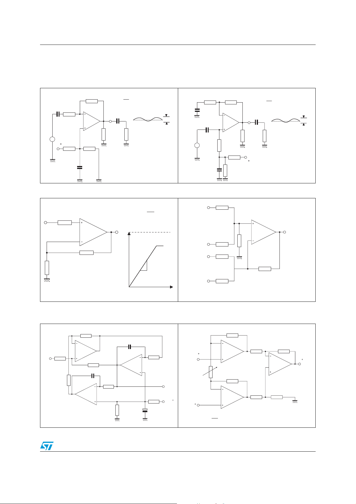
LM2902W Typical single-supply applications
4 Typical single-supply applications
Figure 18. AC coupled inverting amplifier Figure 19. AC coupled non-inverting amplifier
R
f
100 k
Ω
R1
C
10 kΩ
I
1/4
LM2902
R
B
e
~
I
R2
100 k
V
CC
C1
10 μF
6.2 kΩ
R3
100 k
Ω
Ω
R
f
A=-
V
R1
(as shown A = -10)
V
C
o
0
e
o
R
L
10 kΩ
C1
0.1 μF
2V
PP
R1
100 k
C
I
e
I
~
1 MΩ
C2
10
R2
1 M
Ω
1/4
LM2902
6.2 k
Ω
R
B
Ω
R2
A=1+
V
R1
(as shown A = 11)
V
C
o
0
e
o
R
L
10 kΩ
2 V
PP
R3
R4
100 k
Ω
V
CC
R5
100 k
μF
Ω
Figure 20. Non-inverting DC gain Figure 21. DC summing amplifier
100 k
Ω
1
e
Ω
1/4
LM2902
100 k
100 k
Ω
2
O
10 k
R2
A
=1+
V
Ω
e
O
1/4
LM2902
+5 V
R1
(Asshown = 101)
A
V
e
e
100 k
Ω
3
100 k
Ω
4
eo = e1 + e2 - e3 - e4
where (e1 + e2) (e3 + e4)
to keep eo 0 V≥≥
100 k
Ω
10 k
R1
R2
1 M
Ω
Ω
(V)
O
e
e
0
e
(mV)
I
e
Figure 22. Active bandpass filter Figure 23. High input Z adjustable gain DC
instrumentation amplifier
2R1
R2
100 k
1/4
LM2902
Gain adjust
100 k
1/4
LM2902
R1
Ω
R3
100 k
Ω
R5
Ω
R6
100 k
Ω
100 k
1/4
LM2902
R7
100 k
R4
Ω
e
Ω
R1
Ω
100 k
C1
330 pF
1/4
e
1
10 k
LM2902
R3
Ω
Fo = 1 kHz
Q = 50
Av = 100 (40 dB)
10 M
1/4
LM2902
R4
Ω
C2
330 pF
R6
470 kΩ
R8
100 k
1/4
LM2902
Ω
10 μF
R5
470 kΩ
e
O
R7
100 k
Ω
V
C3
CC
e
1
R2
Ω
2 k
e
2
If R1 = R5 and R3 = R4 = R6 = R7
eo = [ 1 + ] (e2 - e1)
As shown eo = 101 (e2 - e1)
O
Doc ID 9922 Rev 8 9/17

Typical single-supply applications LM2902W
Figure 24. High input Z, DC differential
amplifier
R4
100 k
1/4
LM2902
Ω
R1
100 k
Ω
+V1
+V2
eo = [ 1 + ] (e2 - e1)
R4
R3
As shown eo = (e2 - e1)
R2
100 k
1/4
LM2902
Ω
R3
100 k
Ω
Figure 26. Using symmetrical amplifiers to
reduce input current (general
concept)
I
e
I
I
B
I
B
2N 929
LM2902
1/4
I
e
o
Figure 25. Low drift peak detector
I
B
I
B
C
*
B
2I
2N 929
1/4
LM2902
e
I
Z
I
V
o
* Polycarbonate or polyethylene
1 μF
1 M
2I
R
Ω
B
1/4
LM2902
I
3R
3 M
I
0.00
B
B
Ω
Z
o
1 μF
1/4
LM2902
Inputcurrent
compensation
e
o
1.5 M
0.001 μF
I
3 M
B
1/4
Ω
LM2902
I
Aux. amplifier for input
B
current compensation
I
B
Ω
10/17 Doc ID 9922 Rev 8

LM2902W Macromodel
5 Macromodel
An accurate macromodel of the LM2902W is available on STMicroelectronics’ web site at
www.st.com. This model is a trade-off between accuracy and complexity (that is, time
simulation) of the LM2902W operational amplifiers. It emulates the nominal performances of
a typical device within the specified operating conditions mentioned in the datasheet. It also
helps to validate a design approach and to select the right operational amplifier, but it does
not replace on-board measurements.
Doc ID 9922 Rev 8 11/17

Package information LM2902W
6 Package information
In order to meet environmental requirements, ST offers these devices in different grades of
ECOPACK
specifications, grade definitions and product status are available at: www.st.com.
ECOPACK
®
packages, depending on their level of environmental compliance. ECOPACK®
®
is an ST trademark.
6.1 DIP14 package information
Figure 27. DIP14 package mechanical drawing
Table 4. DIP14 package mechanical data
Dimensions
Ref.
Min. Typ. Max. Min. Typ. Max.
a1 0.51 0.020
B 1.39 1.65 0.055 0.065
b0.5 0.020
b1 0.25 0.010
D200.787
E8.5 0.335
e 2.54 0.100
e3 15.24 0.600
F 7.1 0.280
I 5.1 0.201
L3.3 0.130
Z 1.27 2.54 0.050 0.100
Millimeters Inches
12/17 Doc ID 9922 Rev 8

LM2902W Package information
6.2 SO-14 package information
Figure 28. SO-14 package mechanical drawing
Table 5. SO-14 package mechanical data
Dimensions
Ref.
Min. Typ. Max. Min. Typ. Max.
A1.750.068
a1 0.1 0.2 0.003 0.007
a2 1.65 0.064
b 0.35 0.46 0.013 0.018
b1 0.19 0.25 0.007 0.010
C0.5 0.019
c1 45° (typ.)
D 8.55 8.75 0.336 0.344
E 5.8 6.2 0.228 0.244
e 1.27 0.050
e3 7.62 0.300
F 3.8 4.0 0.149 0.157
G 4.6 5.3 0.181 0.208
Millimeters Inches
L 0.5 1.27 0.019 0.050
M0.680.026
S 8° (max.)
Doc ID 9922 Rev 8 13/17

Package information LM2902W
6.3 TSSOP14 package information
Figure 29. TSSOP14 package mechanical drawing
A2
A
A1
b
e
D
c
E1
K
L
E
PIN 1 IDENTIFICATION
Table 6. TSSOP14 package mechanical data
1
Dimensions
Ref.
Millimeters Inches
Min. Typ. Max. Min. Typ. Max.
A 1.2 0.047
A1 0.05 0.15 0.002 0.004 0.006
A2 0.8 1 1.05 0.031 0.039 0.041
b 0.19 0.30 0.007 0.012
c 0.09 0.20 0.004 0.0089
D 4.9 5 5.1 0.193 0.197 0.201
E 6.2 6.4 6.6 0.244 0.252 0.260
E1 4.3 4.4 4.48 0.169 0.173 0.176
e 0.65 BSC 0.0256 BSC
K0° 8°0° 8°
L1 0.45 0.60 0.75 0.018 0.024 0.030
14/17 Doc ID 9922 Rev 8

LM2902W Ordering information
7 Ordering information
Table 7. Order codes
Order code
LM2902WN
LM2902WD/DT SO-14
LM2902WDT
LM2902AWDT
(1)
(1)
LM2902WPT TSSOP14
LM2902WYPT
LM2902AWYPT
1. Qualification and characterization according to AEC Q100 and Q003 or equivalent, advanced screening
according to AEC Q001 & Q 002 or equivalent.
(1)
(1)
Temperature
range
-40°C to +125°C
Package Packing Marking
DIP14 Tube 2902W
SO-14
(Automotive grade level)
SO-14
(Automotive grade level)
TSSOP14
(Automotive grade level)
TSSOP14
(Automotive grade level)
Tape & reel
Tape & reel
2902W
2902WY
2902AWY
2902W
2902WY
2902AWY
Doc ID 9922 Rev 8 15/17

Revision history LM2902W
8 Revision history
Table 8. Document revision history
Date Revision Changes
01-Sep-2003 1 Initial release.
Table data reformatted for easier use in Electrical characteristics on
01-Nov-2005 2
01-Jan-2006 3
page 4.
Minor grammatical and formatting changes throughout.
LM2902WYPT PPAP reference inserted in order codes table, see
Section 7 on page 15.
01-May-2006 4
20-Jul-2007 5
15-Jan-2008 6 Corrected footnotes for automotive grade order codes.
17-Oct-2008 7
16-Feb-2012 8
Minimum value of slew rate at 25°C and on full temperature range
added in Table 3 on page 4.
Corrected document title to “quad operational amplifier”.
Corrected ESD value for HBM to 800V.
Corrected thermal resistance junction to ambient values in Tab le 1 :
Absolute maximum ratings.
Updated electrical characteristics curves.
Added Section 5: Macromodel.
Added automotive grade order codes in Section 7 on page 15.
Added enhanced Vio version: LM2902AW.
Corrected V
Modified Chapter 5: Macromodel.
Deleted LM2902WYD and LM2902AWYD order codes from Ta bl e 7
and modified status of LM2902WYPT and LM2902AWYPT order
codes.
min parameter at Vcc=5V in Table 3 on page 4.
OH
16/17 Doc ID 9922 Rev 8

LM2902W
Please Read Carefully:
Information in this document is provided solely in connection with ST products. STMicroelectronics NV and its subsidiaries (“ST”) reserve the
right to make changes, corrections, modifications or improvements, to this document, and the products and services described herein at any
time, without notice.
All ST products are sold pursuant to ST’s terms and conditions of sale.
Purchasers are solely responsible for the choice, selection and use of the ST products and services described herein, and ST assumes no
liability whatsoever relating to the choice, selection or use of the ST products and services described herein.
No license, express or implied, by estoppel or otherwise, to any intellectual property rights is granted under this document. If any part of this
document refers to any third party products or services it shall not be deemed a license grant by ST for the use of such third party products
or services, or any intellectual property contained therein or considered as a warranty covering the use in any manner whatsoever of such
third party products or services or any intellectual property contained therein.
UNLESS OTHERWISE SET FORTH IN ST’S TERMS AND CONDITIONS OF SALE ST DISCLAIMS ANY EXPRESS OR IMPLIED
WARRANTY WITH RESPECT TO THE USE AND/OR SALE OF ST PRODUCTS INCLUDING WITHOUT LIMITATION IMPLIED
WARRANTIES OF MERCHANTABILITY, FITNESS FOR A PARTICULAR PURPOSE (AND THEIR EQUIVALENTS UNDER THE LAWS
OF ANY JURISDICTION), OR INFRINGEMENT OF ANY PATENT, COPYRIGHT OR OTHER INTELLECTUAL PROPERTY RIGHT.
UNLESS EXPRESSLY APPROVED IN WRITING BY TWO AUTHORIZED ST REPRESENTATIVES, ST PRODUCTS ARE NOT
RECOMMENDED, AUTHORIZED OR WARRANTED FOR USE IN MILITARY, AIR CRAFT, SPACE, LIFE SAVING, OR LIFE SUSTAINING
APPLICATIONS, NOR IN PRODUCTS OR SYSTEMS WHERE FAILURE OR MALFUNCTION MAY RESULT IN PERSONAL INJURY,
DEATH, OR SEVERE PROPERTY OR ENVIRONMENTAL DAMAGE. ST PRODUCTS WHICH ARE NOT SPECIFIED AS "AUTOMOTIVE
GRADE" MAY ONLY BE USED IN AUTOMOTIVE APPLICATIONS AT USER’S OWN RISK.
Resale of ST products with provisions different from the statements and/or technical features set forth in this document shall immediately void
any warranty granted by ST for the ST product or service described herein and shall not create or extend in any manner whatsoever, any
liability of ST.
ST and the ST logo are trademarks or registered trademarks of ST in various countries.
Information in this document supersedes and replaces all information previously supplied.
The ST logo is a registered trademark of STMicroelectronics. All other names are the property of their respective owners.
© 2012 STMicroelectronics - All rights reserved
STMicroelectronics group of companies
Australia - Belgium - Brazil - Canada - China - Czech Republic - Finland - France - Germany - Hong Kong - India - Israel - Italy - Japan -
Malaysia - Malta - Morocco - Philippines - Singapore - Spain - Sweden - Switzerland - United Kingdom - United States of America
www.st.com
Doc ID 9922 Rev 8 17/17
 Loading...