

Page 1
LM2889 TV Video Modulator
General Description
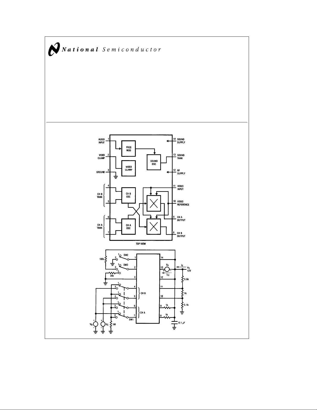
The LM2889 is designed to interface audio and video signals to the antenna terminals of a TV receiver. It consists of
a sound subcarrier oscillator and FM modulator, video
clamp, and RF oscillators and modulators for two low-VHF
channels.
The LM2889 allows video information from VTRs, video disk
systems, games, test equipment, or similar sources to be
displayed on black and white or color TV receivers.
Block and Connection Diagrams (Dual-In-Line Package)
Features
Y
Pin for pin compatible with LM1889 RF section
Y
Low distortion FM sound modulator (less than 1%
THD)
Y
Video clamp for AC-coupled video
Y
Low sound oscillator harmonic levels
Y
10V to 16V supply operation
Y
DC channel switching
Y
Excellent oscillator stability
Y
Low intermodulation products
LM2889 TV Video Modulator
December 1994
Order Number LM2889N
See NS Package Number N14A
DC Test Circuit
TL/H/5079– 1
C
1995 National Semiconductor Corporation RRD-B30M115/Printed in U. S. A.
TL/H/5079
Page 2
Absolute Maximum Ratings
If Military/Aerospace specified devices are required,
please contact the National Semiconductor Sales
Office/Distributors for availability and specifications.
Supply Voltage 18V
Power Dissipation Package (Note 1) 700 mW
Operating Temperature Range 0
§
DC
Ctoa70§C
Storage Temperature Range
(V14–V13) Max
(V12–V8) Max 7V
(V12–V9) Max 7V
b
55§Ctoa150§C
g
5V
DC
DC
DC
Lead Temperature (Soldering, 10 seconds) 260§C
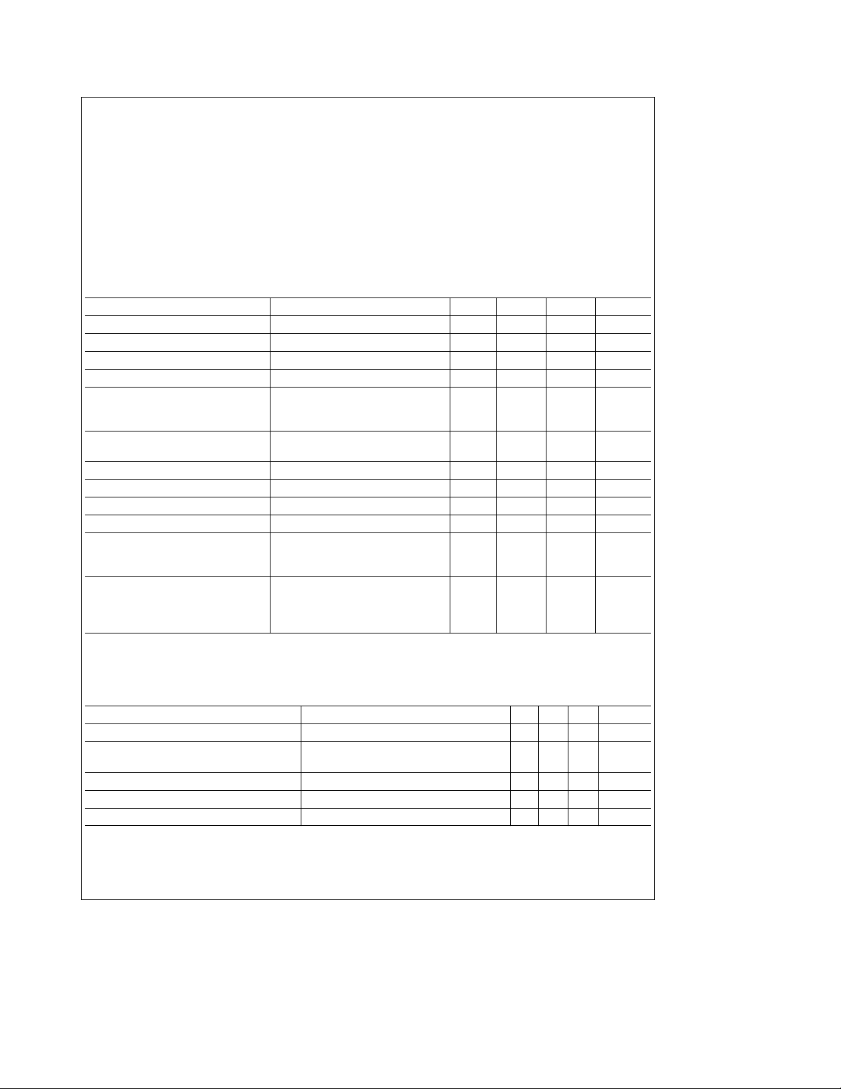
DC Electrical Characteristics
(DC test circuit, all switches normally pos. 1, V
e
S
Parameter Conditions Min Typ Max Units
Supply Current I
Sound Oscillator Current DI
Sound Oscillator Zener Current I
Sound Modulator Audio Current DI
S
13
13
Change VAfromb2V toa2V 0.2 0.35 0.6 mA
Change SW2 from Pos. 1 to Pos. 2 0.9 mA
13
Video Clamp Voltage V2
Unloaded 5.0 5.25 5.5 V
Loaded SW3 Pos. 3 5.1 V
Video Clamp Capacitor Discharge SW3 Pos. 2
Current (V
S
–V2)/10
5
Ch. A Oscillator OFF Voltage, V6, V7 SW1 Pos. 2 2 mV
Ch. A Oscillator Current Level I
7
e
V
B
Ch. B Oscillator OFF Voltage V4, V5 2 mV
Ch. B Oscillator Current Level I
4
SW1 Pos. 2, V
Ch. A Modulator Conversion Ratio Measure DV9 by Changing from
DV9/(V11-V10) V
e
B
e
V
C
Ch. B Modulator Conversion Ratio SW1 Pos. 2, Measure DV8 by
DV8/(V11–V10) Changing from V
to V
B
V11–V10
e
12V, V
A
e
10V, V
C
e
10V, V
C
10V; Divide by V11–V10
e
11V, V
e
2V, V
V
B
11V 2.5 3.5 5.0 mA
e
B
11V, to V
e
C
e
10V, V
C
e
B
e
10V, V
B
10V; Divide by
e
10V)
C
10 16 25 mA
0.85 mA
20 mA
11V 2.5 3.5 5.0 mA
11V, 0.3 0.50 0.75 V/V
e
11V,
C
0.3 0.50 0.75 V/V
DC
DC
DC
DC
AC Electrical Characteristics (AC test circuit, V
e
12V)
S
Parameter Conditions Min Typ Max Units
Sound Carrier Oscillator Level (V13) 3.4 Vp-p
Sound Modulator Deviation Df/DVIN, SW1 Pos. 2, Change VINfrom 1.4V
to 1.0V, Measure Df at Pin 13, Divide as Shown
250 Hz/mV
Ch. 3 RF Oscillator Level n6, n7 Ch. Sw. Pos. 3, fe61.25 MHz, Use FET Probe 550 mVp-p
Ch. 4 RF Oscillator Level, n4, n5, Ch. Sw. Pos. 4, fe67.25 MHz, Use FET Probe 550 mVp-p
RF Modulator Conversion Gain n
Note 1: For operation in ambient temperatures above 25§C, the device must be derated based on a 150§C maximum junction temperature and a thermal resistance
C/W junction to ambient.
of 80
§
Note 2: Conversion gain shown is measured with 75 X input RF meter which makes the AC RF output load 37.5X.
/(V10±V11) Ch. Sw. Pos. 3, fe61.25 MHz. (Note 2) 10 mVrms/V
OUT
2
Page 3
Design Characteristics (AC test circuit, V
Parameter Typ Units
Sound Modulator Audio THD atg25 kHz Deviation, VINmust be 1 kHz Source, 0.8 %
Demodulate as Shown in
Sound Modulator Input Impedance (Pin 1) 1.5 kX
Sound Modulator Bandwidth 100 kHz
Oscillator Supply Dependence, Sound Carrier, RF See Curves
Oscillator Temperature Dependence (IC Only)
Sound Carrier
RF
RF Oscillator Maximum Operating Frequency (Temperature Stability Degraded) 100 MHz
RF Modulator
Carrier Suppression (Adjust Video Bias for Minimum RF Carrier at n
and Reference to n
Information, RF Modulation Section)
3.58 MHz Differential Gain 5 %
Differential Phase 3 degrees
2.5V Vp-p Video, 87.5% Mod
Output Harmonics below RF Carrier
2nd, 3rd
4th and Above
Input Impedance, Pin 10, Pin 11 1 MX//2 pF
Figure 1
with 3V Offset at Pins 10 and 11, See Applications
OUT
e
12V)
S
b
15 ppm/§C
b
50 ppm/§C
OUT
30 dB
b
12 dB
b
20 dB
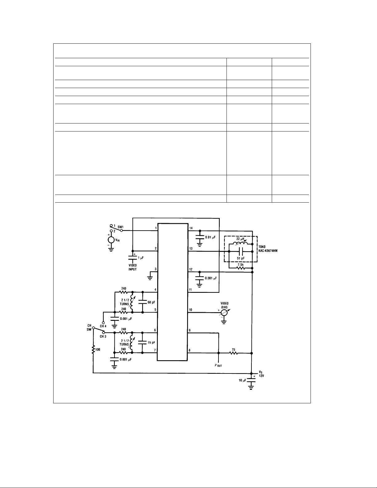
AC Test Circuit
TL/H/5079– 2
3
Page 4
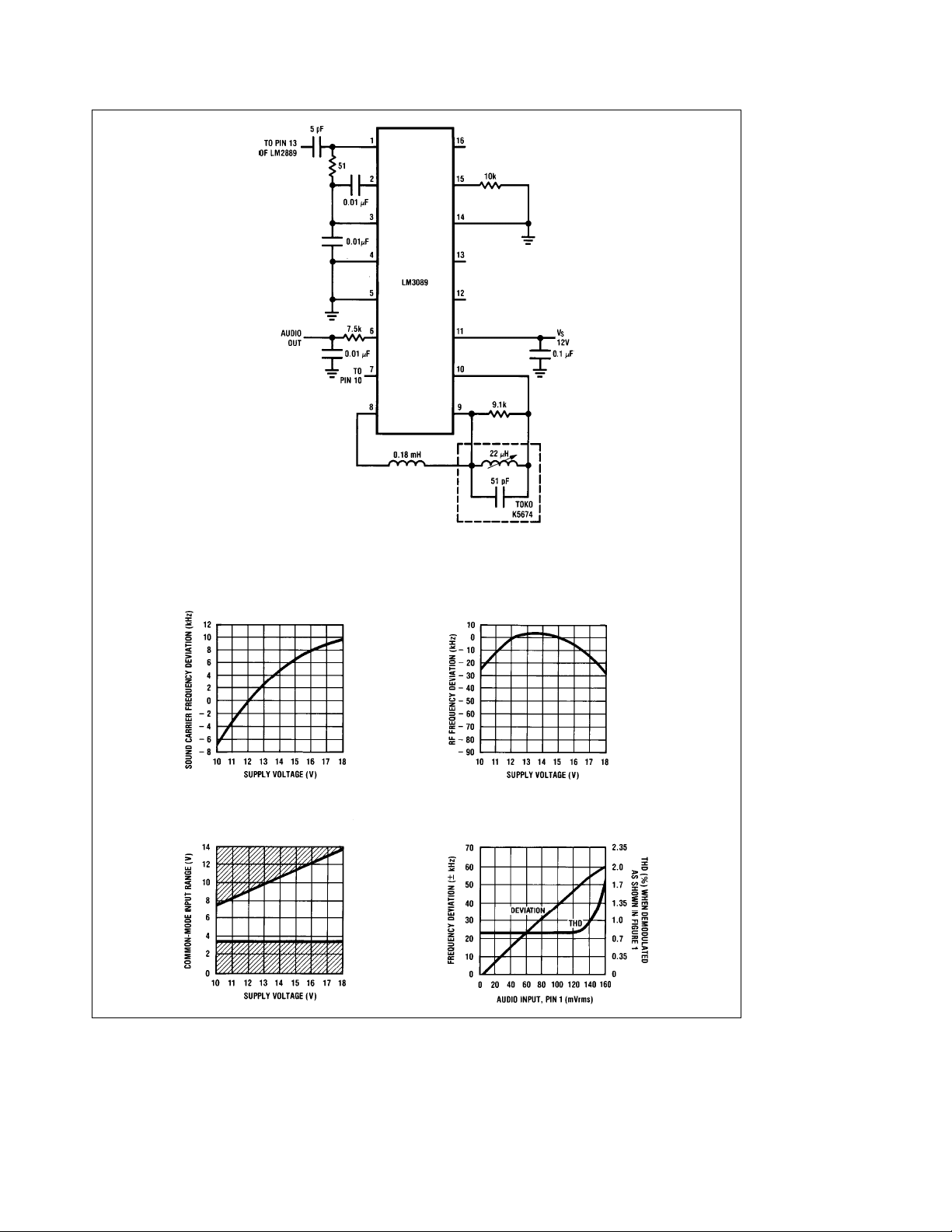
Test Circuit
FIGURE 1. 4.5 MHz Sound FM Demodulator
Typical Performance Characteristics (Refer to AC test circuit unless noted)
Sound Carrier Oscillator
Supply Dependence
e
(f
4.5 MHz, Pin 1 Open)
O
RF Modulator CommonMode Input Range
Pins 10, 11 (Circuit
Diagrams)
RF Oscillator Frequency
Supply Dependence
e
(f
67.25 MHz)
O
FM Sound Modulator
Dynamic Characteristics
e
(f
1 kHz)
MOD
TL/H/5079– 3
TL/H/5079– 4
4
Page 5
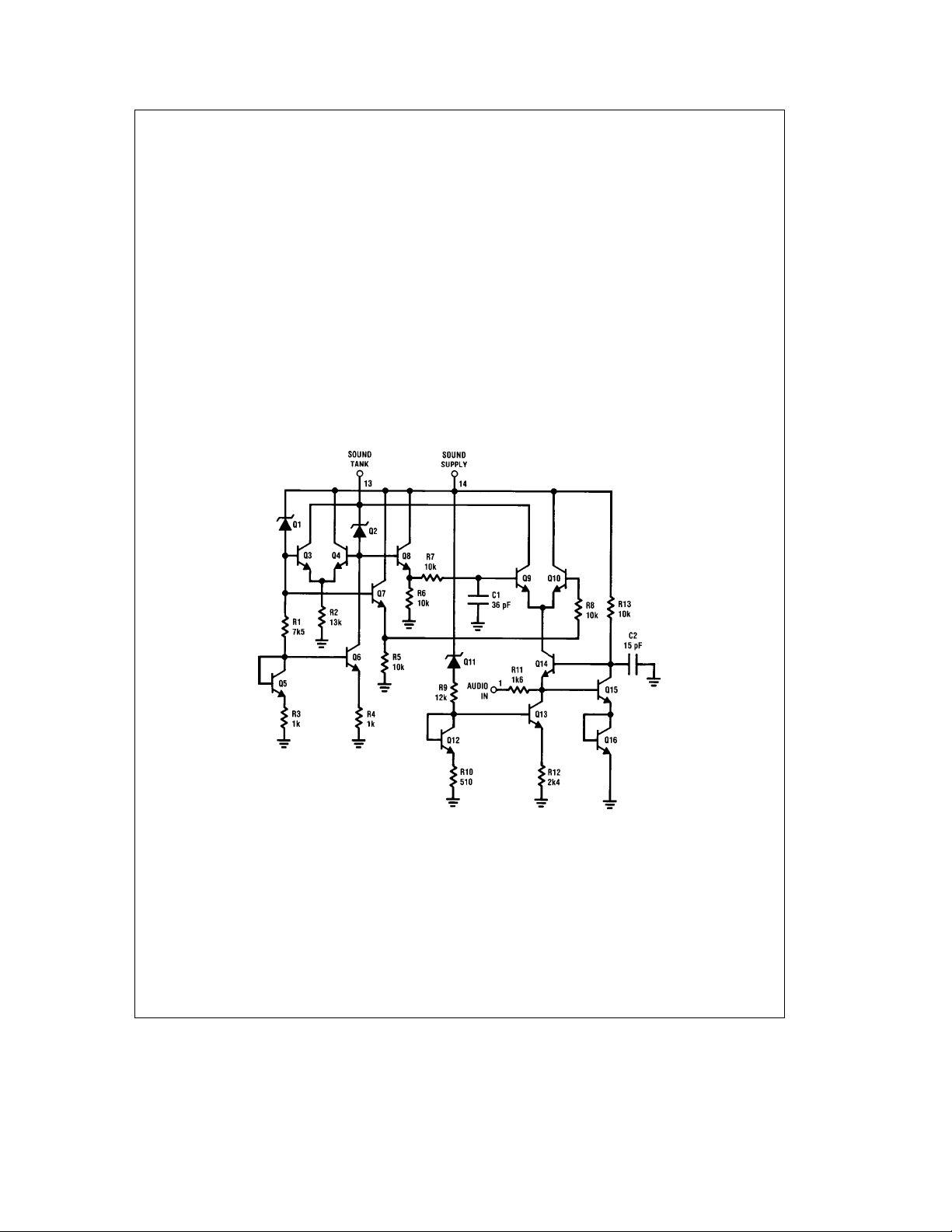
Circuit Description (Refer to Circuit Diagrams)
The sound carrier oscillator is formed by differential amplifier Q3, Q4 operated with positive feedback from the pin 13
tank to the base of Q4. Frequency modulation is obtained
by varying the 90 degree phase shifted current of Q9. Q14’s
emitter is a virtual ground, so the voltage at pin 1 determines the current R11, which ultimately modulates the collector current of Q9.
The video clamp is comprised of devices Q58-Q60. The
clamp voltage is set by resistors R40, R41, R49, and R50.
The DV
rent. Q59 and the above mentioned resistor string help
maintain a temperature stable clamp voltage.
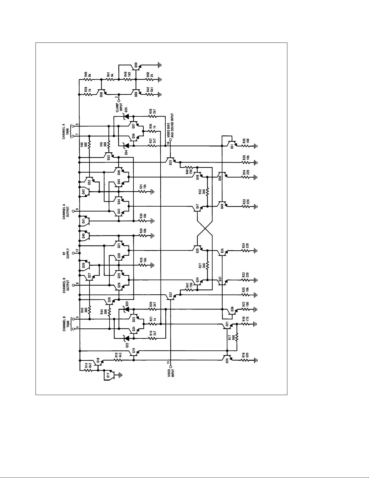
The channel B oscillator consists of devices Q24 and Q25
cross-coupled through level-shift zener diodes Q22 and
Q23. A current regulator consisting of devices Q17–Q21 is
used to achieve good RF stability over temperature and
/R42 current sets the capacitor discharge cur-
BE
Circuit Diagrams
supply. The channel B modulator consists of multiplier devices Q28 – Q31, Q34 and Q35. The top quad is coupled to
the channel B tank through isolating devices Q26 and Q27.
A DC potential between pins 10 and 11 offsets the lower
pair to produce an output RF carrier at pin 8. That carrier is
then modulated by both the sound subcarrier at pin 10 and
the composite video signal at pin 11. The channel A modulator shares pin 10 and 11 buffers, Q32 and Q33, with channel B and operates in an identical manner.
The current flowing through channel B oscillator diodes
Q22, Q23 is turned around in Q36 –Q38 to source current
for the channel B RF modulator. In the same manner, the
channel A oscillator Q54–Q57 uses turn-around Q49 – Q51
to source the channel A modulator. One oscillator at a time
may be activated by its current turn-around, and the other
oscillator/modulator combination remains off.
TL/H/5079– 5
5
Page 6
Circuit Diagrams (Continued)
TL/H/5079– 6
6
Page 7
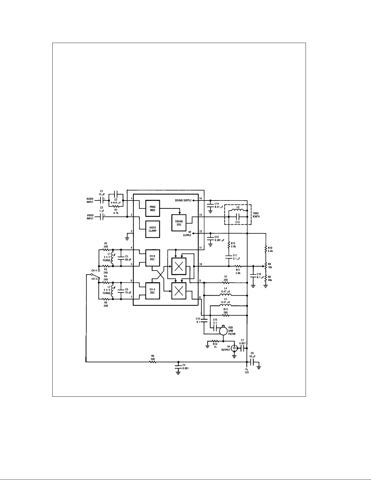
Applications Information
SOUND FM MODULATOR
Frequency deviation is determined by the Q of the tank circuit at pin 13 and the current entering the audio input, pin 1.
This current is set by the input voltage V
impedance (1.5 kX), and any impedance network connected externally. A signal of 60 mVrms at pin 1 will yield about
g
25 kHz deviation when configured as shown in
VIDEO CLAMP
When video is not available at DC levels within the RF modulator common-mode range, or if the DC level of the video is
not temperature stable, then it should be AC-coupled as
shown in the typical applications circuit (
clamp holds the horizontal sync pulses at 5.2V for V
The clamp coupling capacitor is charged during every sync
pulse and discharged when video information is present.
The discharge current is approximately 20 mA. This current
and the amount of acceptable tilt over a line of video determines the value of the coupling capacitor C1. For most applications 1 mF is sufficient.
, the device input
IN
Figure 2
Figure 2
). The
e
S
12V.
Typical Application
RF MODULATION
Two RF channels are available, with carrier frequencies up
to 100 MHz being determined by L-C tank circuits at pins
4/ 5 and 6/7. The signal inputs (pins 10 and 11) are common to both modulators, but removing the power supply
from an RF oscillator will also disable that modulator.
.
The offset between the two signal pins determines the level
of the RF carrier output. To preserve the DC content of the
video signal, amplitude modulation of the RF carrier is done
in one direction only, with increasing video (toward peak
white) decreasing the carrier level. This means the active
composite video signal at pin 11 must be offset with respect
to pin 10 and the sync pulse should produce the largest
offset.
The largest video signal (peak white) should not be able to
suppress the carrier completely, particularly if sound transmission is needed. This requires that pin 10 be biased
above the largest expected video signal. Because peak
white level is often difficult to define, a good rule to follow is
to bias pin 10 at a level which is four times the sync amplitude above the sync tip level at pin 11. For example, the DC
bias at pin 10 with 0.5V sync clamped to 5.2V on pin 11,
should be 5.2
a
(4c0.5)e7.2V.
FIGURE 2. Two Channel Video Modulator with FM Sound
7
TL/H/5079– 7
Page 8
Applications Information (Continued)
When the signal inputs are exactly balanced, ideally there is
no RF carrier at the output. Circuit board layout is critical to
this measurement. For optimum performance, the output
and supply decoupling circuitry should be configured as
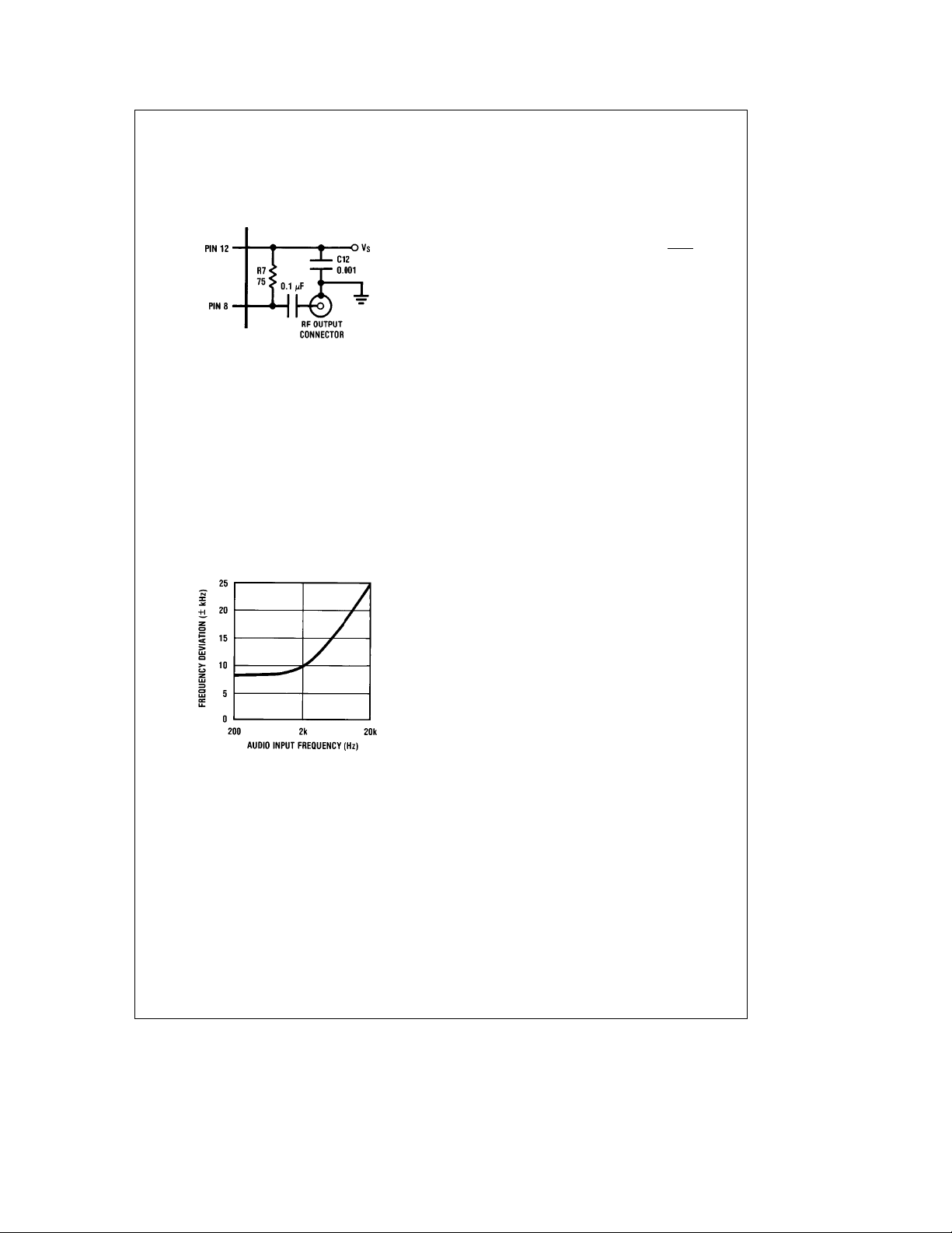
shown in
Figure 3
.
RF decouple supply directly to output ground.
FIGURE 3. Correct RF Supply Decoupling
The video clamp level is derived from a resistive divider connected to supply (V
pin 10, which is biased externally, should also be referenced
to supply (see
Pin Description (Refer to
Pin 1ÐAudio Input: Pin 1 is the audio input to the sound
FM generator. Frequency deviation is proportional to the
signal at this pin. A pre-emphasis network comprised of R1,
C2, and the device input impedance yields the following response with an 80 mVrms audio input.
Increasing R1 lowers the boost frequency, and decreases
deviation below the boost frequency. Increasing C2 only
lowers the boost frequency. C1 is a coupling capacitor, and
must be a low impedance compared to the sum of R1 and
the device input impedance (1.5 kX).
). To maintain good supply rejection,
S
Figure 2
).
Figure 2
Pre-Emphasis Network
Response
TL/H/5079– 8
)
TL/H/5079– 9
Pin 2ÐVideo Clamp: The video clamp restores the DC
component to AC-coupled video. The video is AC-coupled
to the clamp via C3. Decreasing C3 will cause a larger tilt
between vertical sync pulses in the clamped video waveform.
Pin 3ÐGround: Although separate on the chip level, all
ground terminate at pin 3.
Pins 4/5ÐChannel 4 Oscillator: Pins 4 and 5 are the collector outputs of the channel 4 oscillator. L1 and C5 set the
oscillator frequency defined by f
ing L1 will decrease the oscillator frequency while decreasing L1 will increase the oscillator frequency. Decreasing C5
will increase the oscillator frequency and lower the tank Q
causing possible drift problems. R2 and R3 are the oscillator
loads which determine the oscillator amplitude and the tank
Q. Increasing these resistors increases the Q and the oscillator amplitude, possibly overdriving the RF modulator,
which will increase output RF harmonics. Decreasing R2
and R3 reduces the tank Q and may cause increased drift.
C4 is an RF decoupling capacitor. Increasing C4 may result
in less effective decoupling at RF. Decreasing C4 may introduce RF to supply coupling.
Pins 6/7ÐChannel 3 Oscillator; Pins 6 and 7 are the channel 3 oscillator outputs. Every component at these pins has
the same purpose and effect as those at pins 4 and 5.
Pin 8ÐChannel 4 RF Output: Pin 8 is the channel 4 RF
output and R13 is the load resistor. The RF signal is AC
coupled via C15 to the output filter which is a two channel
VSB filter. L5 is parallel resonant with the filter input capacitance minimizing loss in the output network. R14 terminated
the filter output.
Pin 9ÐChannel 3 RF Output: Pin 9 is the channel 3 RF
output with all components performing the same functions
as those in the pin 8 description.
Pin 10ÐRF Modulator Sound Subcarrier Input: Pin 10 is
one of the RF modulator inputs and may be used for video
or sound. It is used as a sound subcarrier input in
R8, R9, and R10 set the DC bias on this pin which determines the modulation depth of the RF output (see Application Notes). R12 and C11 AC-couple the sound subcarrier
from the sound modulator to the RF modulator. R12 and
R11 form a resistive divider that determines the level of
sound at pin 10, which in turn sets the picture carrier to
sound subcarrier ratio. Increasing the ratio of R11/R12 will
increase the sound subcarrier at the output. C10 forms an
AC ground, preventing R8, R9, and R10 from having any
effects on the circuit other than setting the DC potential at
pin 10. R11 and R12 also effect the FM sound modulator
(see pin 13 description).
e
0.159/SL1C5. Increas-
O
Figure 2
.
8
Page 9
Pin Description (Continued)
Pin 11ÐVideo Input: Pin 11, when configured as shown, is
the RF modulator video input. In this application, video is
coupled directly from the video clamp. Alternatively, video
could be DC-coupled directly to pin 11 if it is already within
the DC common-mode input range of the RF modulator (see
curves). In any case, the video sync tip at pin 11 must have
a constant DC level independent of video content. Because
of circuit symmetry, pins 10 and 11 may be interchanged.
Pin 12ÐRF Supply: Pin 12 is the RF supply, with C12 and
C7 serving as RF decouple capacitors. Increasing C12 or
C7 may result in less effective RF decoupling, while decreasing them may cause supply interaction. It is important
that C7 be grounded at the RF output ground.
Pin 13ÐSound Tank: Pin 13 is the collector output of the
sound oscillator. L3 and C13 determine the oscillating frequency by the relationship f
L3 or C13 will lower the operating frequency, while decreasing them will raise the frequency. L3 and C13 also help
define the Q of the tank, on which FM modulator deviation level depends. As C13 increases, Q increases, and
frequency deviation decreases. Likewise, decreasing C13
increases deviation. The other factor concerning Q is the
e
0.159/SL3C13. Increasing
O
external resistance across the tank. The series combination
a
R11
R12 usually dominates the tank Q. Decreasing this
resistive network will decrease Q and increase deviation. It
should be noted that because the level of phase modulation
of the 4.5 MHz signal remains constant, variation in Q will
not effect distortion of the frequency modulation process if
the audio at pin 1 is left constant. The amplitude of the
sound subcarrier is directly proportional to Q, so increasing
the unloaded Q or either of the resistors mentioned above
will increase the sound subcarrier amplitude. For proper operation of the frequency modulator, the sound subcarrier
amplitude should be greater than 2 Vp-p.
Pin 14ÐSound Supply: Pin 14 is the sound supply and C14
is an RF decouple capacitor. Decreasing C14 may result in
increased supply interaction.
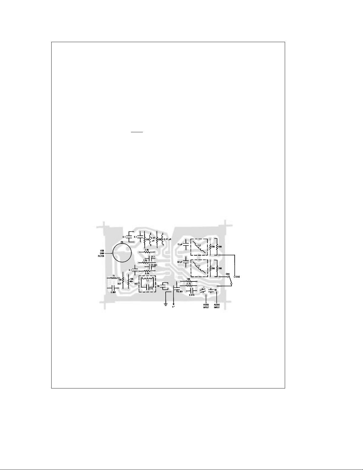
Printed Circuit Layout
Printed circuit board layout is critical in preventing RF feedthrough. The location of RF bypass capacitors on supply is
very important.
layed out circuit board. It is recommended that this layout be
used.
Figure 4
shows an example of a properly
FIGURE 4. Printed Circuit Board and Component Diagram
(Component Side 1X)
9
TL/H/5079– 10
Page 10
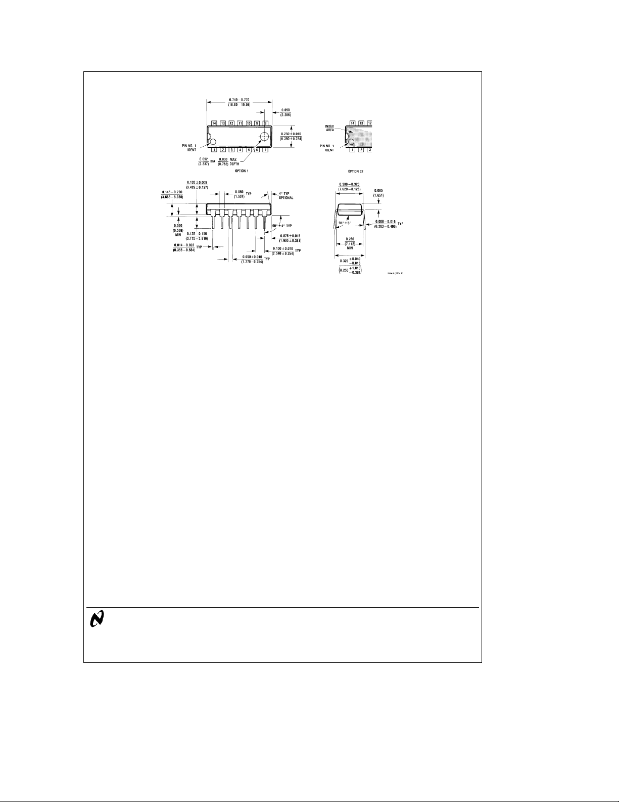
Physical Dimensions inches (millimeters)
LM2889 TV Video Modulator
Molded Dual-In-Line Package (N)
Order Number LM2889N
NS Package Number N14A
LIFE SUPPORT POLICY
NATIONAL’S PRODUCTS ARE NOT AUTHORIZED FOR USE AS CRITICAL COMPONENTS IN LIFE SUPPORT
DEVICES OR SYSTEMS WITHOUT THE EXPRESS WRITTEN APPROVAL OF THE PRESIDENT OF NATIONAL
SEMICONDUCTOR CORPORATION. As used herein:
1. Life support devices or systems are devices or 2. A critical component is any component of a life
systems which, (a) are intended for surgical implant support device or system whose failure to perform can
into the body, or (b) support or sustain life, and whose be reasonably expected to cause the failure of the life
failure to perform, when properly used in accordance support device or system, or to affect its safety or
with instructions for use provided in the labeling, can effectiveness.
be reasonably expected to result in a significant injury
to the user.
National Semiconductor National Semiconductor National Semiconductor National Semiconductor
Corporation Europe Hong Kong Ltd. Japan Ltd.
1111 West Bardin Road Fax: (
Arlington, TX 76017 Email: [email protected] Ocean Centre, 5 Canton Rd. Fax: 81-043-299-2408
Tel: 1(800) 272-9959 Deutsch Tel: (
Fax: 1(800) 737-7018 English Tel: (
National does not assume any responsibility for use of any circuitry described, no circuit patent licenses are implied and National reserves the right at any time without notice to change said circuitry and specifications.
Fran3ais Tel: (
Italiano Tel: (
a
49) 0-180-530 85 86 13th Floor, Straight Block, Tel: 81-043-299-2309
a
49) 0-180-530 85 85 Tsimshatsui, Kowloon
a
49) 0-180-532 78 32 Hong Kong
a
49) 0-180-532 93 58 Tel: (852) 2737-1600
a
49) 0-180-534 16 80 Fax: (852) 2736-9960
 Loading...