

ST LM2901H User Manual
High temperature, low-power quad voltage comparators
Features
■ Wide single supply voltage range or dual
supplies for all devices: +2 V to +36 V or ±1 V
to ±18 V
■ Very low supply current (1.1 mA) independent
of supply voltage (1.4 mW/comparator at +5 V)
■ Low input bias current: 25 nA typ.
■ Low input offset current: ±5 nA typ.
■ Input common-mode voltage range includes
ground
■ Low output saturation voltage:
250 mV typ. (I
■ Differential input voltage range equal to the
supply voltage
■ TTL, DTL, ECL, MOS, CMOS compatible
outputs
= 4 mA)
O
LM2901H
Datasheet − production data
D
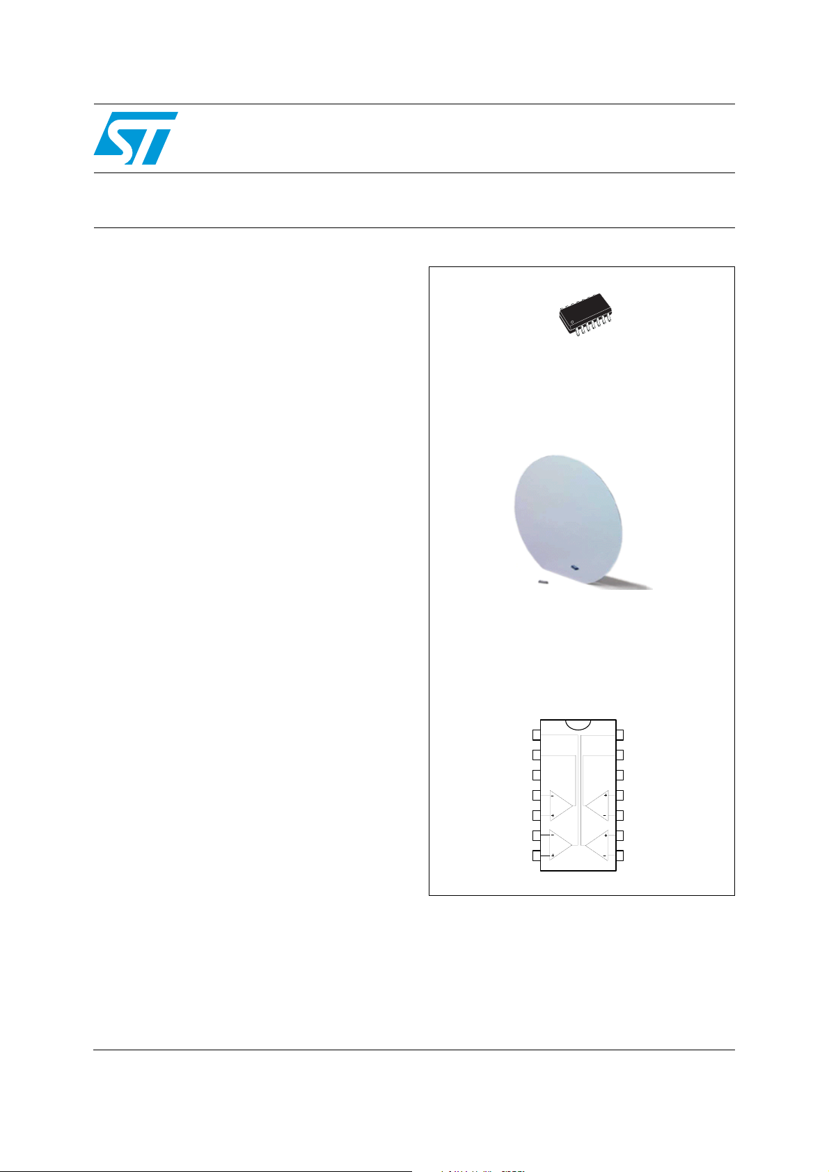
SO-14
(Plastic micropackage)
Description
This device consists of four independent precision
voltage comparators. All these comparators are
designed specifically to operate from a single
power supply over a wide range of voltages.
Operation from split power supplies is also
possible.
These comparators also have a unique
characteristic in that the input common-mode
voltage range includes ground even though
operated from a single power supply voltage.
Output 2
Output 1
Inverting input 1
Non-inverting input 1
Inverting input 2
Non-inverting input 2
Wafer form
Pin connections (top view)
1
2
+
V
3
CC
4
5
6
7
14
Output 3
13
Output 4
12
V
11
Non-inverting input 4
10
Inverting input 4
9
Non-inverting input 3
8
Inverting input 3
-
CC
March 2012 Doc ID 9874 Rev 5 1/10
This is information on a product in full production.
www.st.com
10
Absolute maximum ratings and operating conditions LM2901H
1 Absolute maximum ratings and operating conditions
Table 1. Absolute maximum ratings (AMR)
Symbol Parameter Value Unit
V
CC
V
ID
V
in
R
thja
R
thjc
T
ESD
T
stg
1. Short-circuit from the output to V
output current is approximately 20 mA, independent of the magnitude of V
2. Short-circuits can cause excessive heating and destructive dissipation. Values are typical.
3. Human body model: A 100 pF capacitor is charged to the specified voltage, then discharged through a
1.5 kΩ resistor between two pins of the device. This is done for all couples of connected pin combinations
while the other pins are floating.
4. Machine model: A 200 pF capacitor is charged to the specified voltage, then discharged directly between
two pins of the device with no external series resistor (internal resistor < 5 Ω). This is done for all couples of
connected pin combinations while the other pins are floating.
5. Charged device model: all pins and the package are charged together to the specified voltage and then
discharged directly to the ground through only one pin. This is done for all pins.
Table 2. Operating conditions
Supply voltage ±18 or 36 V
Differential input voltage ±36 V
Input voltage -0.3 to +36 V
Output short-circuit to ground
Thermal resistance junction to ambient
(1)
(2)
(SO-14)
Thermal resistance junction to case
(2)
(SO-14)
Maximum junction temperature 160 °C
j
HBM: human body model
MM: machine model
CDM: charged device model
(3)
(4)
(5)
20 mA
105 °C/W
31 °C/W
500
100
1500
Storage temperature range -65 to +150 °C
+
can cause excessive heating and eventual destruction. The maximum
CC
CC
+
V
Symbol Parameter Value Unit
+
V
T
CC
oper
Supply voltage 2 to 36 V
Operating free-air temperature range -40 to +150 °C
Input common mode voltage range (V
V
icm
1. The input common-mode voltage of either input signal voltage should not be allowed to go negative by
more than 0.3 V. The upper end of the common-mode voltage range is V
inputs can go to +30 V without damage.
T
T
amb
min
= +25°C
≤ T
amb
≤ T
max
2/10 Doc ID 9874 Rev 5
CC
= 30 V)
(1)
CC
CC
+
-1.5
+
-2
0 to V
0 to V
+
–1.5 V, but either or both
CC
V
LM2901H Circuit schematics
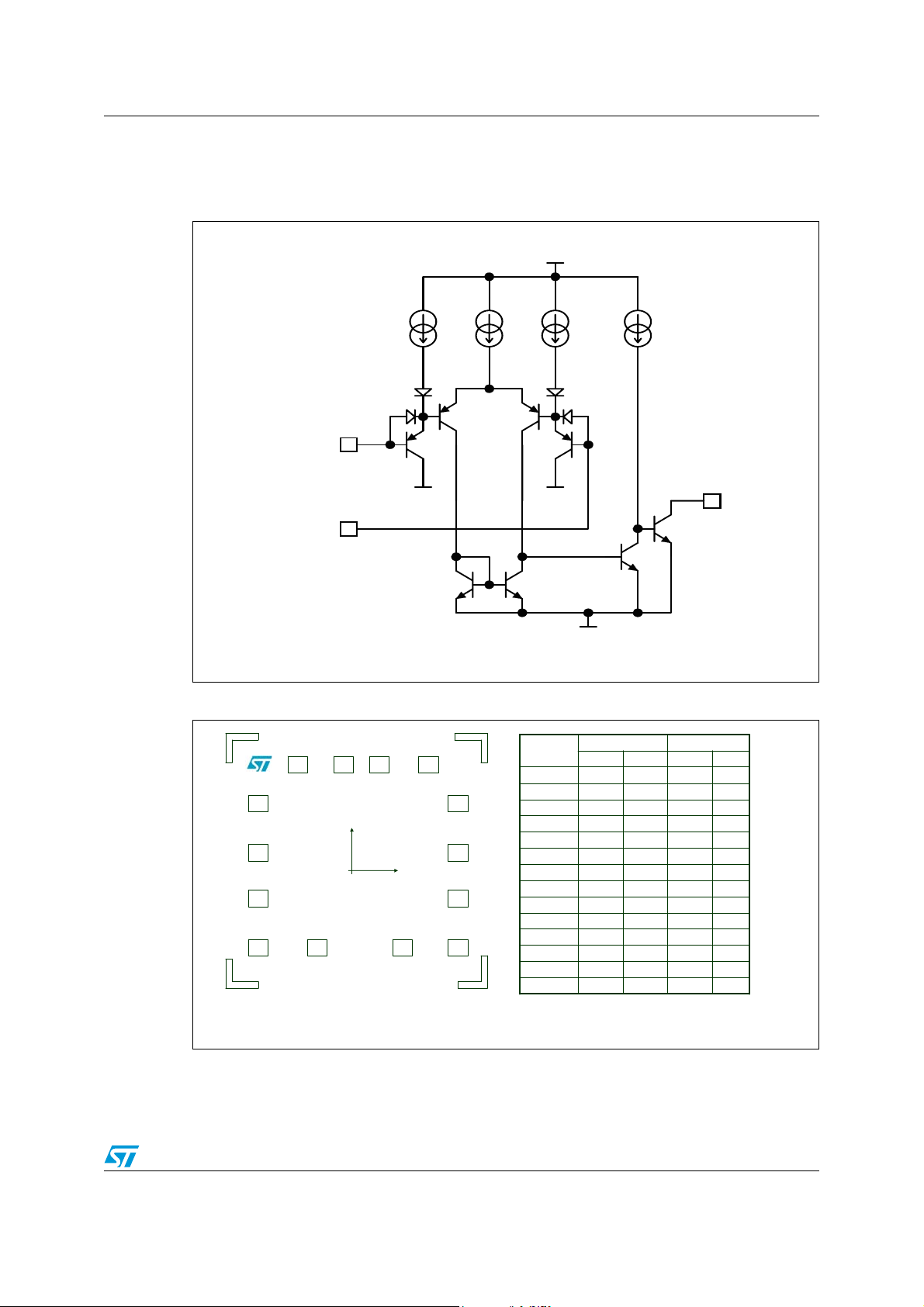
2 Circuit schematics
Figure 1. Schematic diagram (1/4 LM2901)
VCC+
3.5µA 100µA 3.5µA 100µA
Non-Inverting
Input
Inverting
VCC- VCC-
Input
Figure 2. Pad locations
OUT 1 OUT 2 OUT 3 OUT 4
Year
Vcc +
y
E- (1)
x
E+ (1)
E- (2)
The Origin coordinate is at the centre of the die
0339
PD98
Vcc -
E+ (4)
E+ (4)
E+ (3)E+ (2) E- (3)
Vo
VCC-
Pad dimensionPad placementName
Pad dimensionPad placementName
YXYX
YXYX
8080480-40OUT2
8080480-40OUT2
8080480-340OUT1
8080480-340OUT1
8080320-530VCC+
8080320-530VCC+
8080150-530E-(1)
8080150-530E-(1)
8080-150-530E+(1)
8080-150-530E+(1)
8080-480-530E-(2)
8080-480-530E-(2)
8080-480-210E+(2)
8080-480-210E+(2)
8080-480210E-(3)
8080-480210E-(3)
8080480530E+(3)
8080480530E+(3)
8080-150530E-(4)
8080-150530E-(4)
8080150530E+(4)
8080150530E+(4)
8080300530VCC -
8080300530VCC -
8080480430OUT4
8080480430OUT4
8080480150OUT3
8080480150OUT3
All dimensions are specified in micrometers (µm)
Doc ID 9874 Rev 5 3/10
 Loading...