

Low-power quad voltage comparator
Features
■ Wide single supply voltage range or dual
supplies for all devices: +2 V to +36 V or ±1 V
to ±18 V
■ Very low supply current (1.1 mA) independent
of supply voltage (1.4 mW/comparator at +5 V)
■ Low input bias current: 25 nA typ.
■ Low input offset current: ±5 nA typ.
■ Input common-mode voltage range includes
negative rail
■ Low output saturation voltage:
250 mV typ. (I
■ Differential input voltage range equal to the
supply voltage
■ TTL, DTL, ECL, MOS, CMOS compatible
outputs
= 4 mA)
O
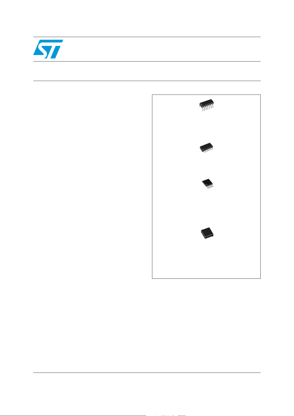
LM2901
N
DIP14
(Plastic package)
D
SO-14
(Plastic micropackage)
P
TSSOP14
(Thin shrink small outline package)
Description
This device consists of four independent precision
voltage comparators, which are designed
specifically to operate from a single supply over a
wide range of voltages. Operation from split
power supplies is also possible.
These comparators also have a unique
characteristic in that the input common-mode
voltage range includes the negative rail even
though operated from a single power supply
voltage.
Q4
QFN16 3x3
(Plastic micropackage)
February 2012 Doc ID 2468 Rev 7 1/17
www.st.com
17
Pin connection and schematic diagram LM2901
1 Pin connection and schematic diagram
Figure 1. Pin connections (top view)
Output 2
Output 1
VCC+
Inverting input 1
Non-inverting input 1
Inverting input 2
Non-inverting input 2
1
2
3
4
5
6
7
14
Output 3
13
Output 4
12
VCC-
11
Non-inverting input 4
10
Inverting input 4
9
Non-inverting input 3
8
Inverting input 3
Figure 2. Schematic diagram
3.5μA
Non-inverting
input
2/17 Doc ID 2468 Rev 7
Inverting
input
V
CC
100 μA
3.5μA
100μA
V
O
V
CC
LM2901 Absolute maximum ratings and operating conditions
2 Absolute maximum ratings and operating conditions
Table 1. Absolute maximum ratings
Symbol Parameter Value Unit
V
CC
V
id
V
in
R
thja
R
thjc
T
j
T
stg
ESD
1. Short-circuits from the output to V
maximum output current is approximately 20 mA, independent of the magnitude of V
2. Short-circuits can cause excessive heating. Destructive dissipation can result from simultaneous shortcircuits on all amplifiers. All values are typical.
Supply voltage ±18 to 36 V
Differential input voltage ±36 V
Input voltage -0.3 to +36 V
Output short-circuit to ground
Thermal resistance junction to ambient
DIP14
SO-14
TSSOP14
QFN16 3x3
Thermal resistance junction to case
DIP14
SO-14
TSSOP14
QFN16 3x3
(1)
(2)
(2)
80
105
100
45
33
31
32
14
°C/W
Maximum junction temperature +150 °C
Storage temperature range -65 to +150 °C
HBM: human body model
MM: machine model
CDM: charged device model
CC
(3)
(4)
(5)
+
can cause excessive heating and eventual destruction. The
500 V
100 V
1500 V
+
.
CC
3. Human body model: a 100 pF capacitor is charged to the specified voltage, then discharged through a
1.5 kΩ resistor between two pins of the device. This is done for all couples of connected pin combinations
while the other pins are floating.
4. Machine model: a 200 pF capacitor is charged to the specified voltage, then discharged directly between
two pins of the device with no external series resistor (internal resistor < 5 Ω). This is done for all couples of
connected pin combinations while the other pins are floating.
5. Charged device model: all pins and the package are charged together to the specified voltage and then
discharged directly to the ground through only one pin. This is done for all pins.
Table 2. Operating conditions
Symbol Parameter Value Unit
V
CC
T
V
icm
oper
Supply voltage
Common mode input voltage range
T
≤ T
amb
≤ T
max
min
Operating free-air temperature range -40 to +125 °C
2 to 32
±1 to ±16
0 to (V
0 to (V
CC
CC
+
+
-1.5)
-2)
V
V
Doc ID 2468 Rev 7 3/17
Electrical characteristics LM2901
3 Electrical characteristics
Table 3. Electrical characteristics at V
CC
+
= 5 V, V
-
= GND, T
CC
amb
= 25° C
(unless otherwise specified)
Symbol Parameter Min. Typ. Max. Unit
V
I
io
I
ib
A
vd
Input offset voltage
io
T
≤ T
min
Input offset current
T
≤ T
min
Input bias current (I
T
≤ T
min
Large signal voltage gain
(VCC = 15 V, RL=15kΩ, Vo= 1 to 11 V)
amb
amb
amb
Supply current (all comparators)
I
CC
V
= +5 V, no load
CC
VCC = +30 V, no load
V
Differential input voltage
id
Low level output voltage
V
OL
Vid = -1V, I
T
≤ T
min
sink
amb
High level output current
I
I
sink
t
OH
res
(V
CC =Vo
T
Output sink current (Vid = -1 V,Vo = 1.5 V) 6 16 mA
Small signal response time
(RL = 5.1 kΩ connected to V
= 30 V, Vid = 1 V)
≤ T
min
amb
Large signal response time
TTL input (V
t
rel
+
)
V
CC
Output signal at 50% of final value
Output signal at 95% of final value
1. At output switch point, VO ≈ 1.4 V, RS = 0 with V
mode range (0 V to V
2. The direction of the input current is out of the IC due to the PNP input stage. This current is essentially
constant, independent of the state of the output, so there is no loading charge on the reference of input
lines.
3. The response time specified is for a 100 mV input step with 5 mV overdrive.
4. Positive excursions of input voltage may exceed the power supply level. As long as the other voltage
remains within the common-mode range, the comparator will provide a proper output state. The low input
voltage state must not be less than –0.3 V (or 0.3 V below the negative power supply, if used).
5. Maximum values are guaranteed by design.
CC
+
–1.5 V).
(1)
≤ T
max
≤ T
max
(2)
+
-
or I
)
I
I
≤ T
max
(3)
= 4 mA
≤ T
max
≤ T
max
(4)
CC
(5)
= +1.4 V, RL=5.1kΩ to
ref
17
15
550
150
25 250
400
25 200 V/mV
1.1
1.3
V
2
2.5
CC
250 400
700
0.1
1
+
)
+
from 5 V to 30 V, and over the full input common-
CC
1.3 µs
500
1
mV
nA
nA
mA
+
V
mV
nA
µA
ns
µs
4/17 Doc ID 2468 Rev 7
LM2901 Electrical characteristics
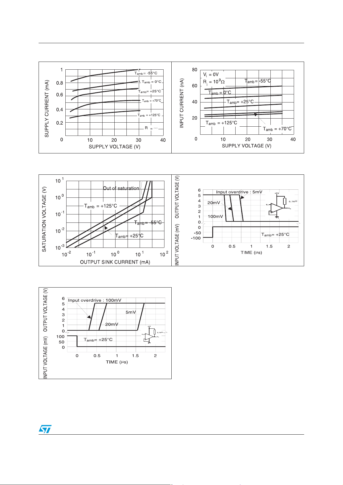
Figure 3. Supply current vs. supply voltage Figure 4. Input current vs. supply voltage
Figure 5. Output saturation voltage vs.
output current
Figure 6. Response time for various input
overdrives - negative transition
Figure 7. Response time for various input
overdrives - positive transition
Doc ID 2468 Rev 7 5/17
Typical application schematics LM2901
4 Typical application schematics
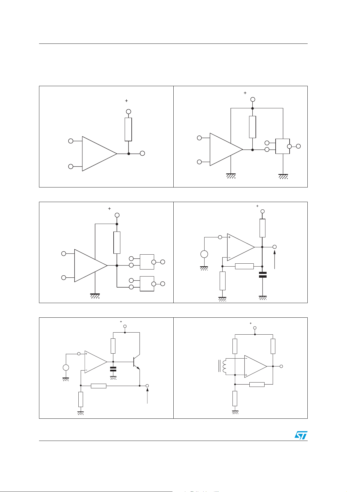
Figure 8. Basic comparator Figure 9. Driving CMOS
5 V
V
= 5 V
CC
100 kΩ
+V
-V
(ref)
(ref)
1/4
LM2901
15 kΩ
+V
(ref)
1/ 4
V
O
-V
(ref)
LM2901
Figure 10. Driving TTL Figure 11. Low frequency op-amp
5 V
+V
-V
(ref)
(ref)
1/ 4
LM2901
5 V
10 kΩ
1/4
LM2901
~
e
l
&
100 kΩ
&
1 kΩ
AV = 100
15 k
0.5 μF
&
Ω
e
o
Figure 12. Low frequency op-amp with boost Figure 13. Transducer amplifier
5 V
(eo = 0 V for el = 0 V)
15 kΩ
1/ 4
LM2901
e
~
l
1 kΩ
100 k
AV = 100
0.5 μF
Ω
2N 2222
e
o
6/17 Doc ID 2468 Rev 7
Magnetic pick-up
10 kΩ
10 kΩ
5 V
1/ 4
LM2901
20 MΩ
3 kΩ
e
o

LM2901 Typical application schematics
Figure 14. Low frequency op-amp with
~
e
l
R
2
R
S
offset adjust
Offset adjust
R
1 MΩ
1
5 V
100 kΩ
1 kΩ
1 MΩ
1/ 4
LM2901
100 kΩ
15 kΩ
0.5μF
R1
5 V
2N 2222
e
o
Figure 15. Zero crossing detector (single
power supply)
5 V
100 kΩ
5.1 kΩ
e
l
5.1 kΩ
1N4148
100 kΩ
1/ 4
LM2901
20 MΩ
10 kΩ
5.1 kΩ
Figure 16. Limit comparator Figure 17. Split-supply applications - zero
crossing detector
V
V
high
V
low
(12 V)
CC
1/ 4
LM2901
1/ 4
LM139
10 kΩ
Lamp
2N 2222
e
~
I
2R
(ref)
e
I
(ref)
S
R
S
~
2R
S
15 V
1/4
LM2901
15 V
5.1 kΩ
e
o
Figure 18. Crystal controlled oscillator Figure 19. Comparator with a negative
reference
V
0.1 μF
200 kΩ
CC
100 kΩ
1/ 4
LM2901
= 15 V
2 kΩ
V
CC
0
e
o
15 V
1/ 4
LM2901
e
200 kΩ
f = 100 kHz
~
I
5 V
15 V
Doc ID 2468 Rev 7 7/17
5.1 kΩ
e
o

Typical application schematics LM2901
Figure 20. Time delay generator
V
=+15V
C C
V
CC
0
Input gating signal
V
CC
V
3
V
V
2
C1
V
1
0
t
t
t
2
1
0
10 kΩ
15 kΩ
200 k
Ω
3 kΩ
10 MΩ
10 kΩ
1/4
V
3
10 kΩ
LM2901
t
t
o
A
V
(ref.)
51 kΩ
V
1/4
C1
10 kΩ
V
2
LM2901
10 MΩ
1/4
LM2901
3 k
V
CC
V
03
t
t
o
3
Ω
V
CC
V
O2
t
t
o
2
0.001μF
3 k
Ω
10 MΩ
51 kΩ
V
t
3
t
t
4
51 kΩ
10 kΩ
1/4
LM2901
1
V
V
CC
O1
t0t
1
Figure 21. Two-decade high-frequency VCO
V
CC
Frequency control
voltage input
Vcontrol
100 kΩ
10 kΩ
0.1 μF
1/ 4
LM2901
500 pF
3 kΩ
5.1 kΩ
0.01 μF
20 kΩ
V
o
control
20 kΩ
+50 V
1/ 4
LM2901
V
CC
50 kΩ
V
=+30V
CC
+250 mV
700 Hz f 100 kHz
100 kΩ
1/ 4
LM2901
V
/2
CC
/2
V
CC
3 kΩ
Output 1
Output 2
8/17 Doc ID 2468 Rev 7

LM2901 Package information
5 Package information
In order to meet environmental requirements, ST offers these devices in different grades of
ECOPACK
specifications, grade definitions and product status are available at: www.st.com.
ECOPACK
®
packages, depending on their level of environmental compliance. ECOPACK®
®
is an ST trademark.
Doc ID 2468 Rev 7 9/17

Package information LM2901
5.1 DIP14 package information
Figure 22. DIP14 package mechanical drawing
Table 4. DIP14 package mechanical data
Dimensions
Millimeters Inches
Ref.
Min. Typ. Max. Min. Typ. Max.
A5.330.21
A1 0.38 0.015
A2 2.92 3.30 4.95 0.11 0.13 0.19
b 0.36 0.46 0.56 0.014 0.018 0.022
b2 1.14 1.52 1.78 0.04 0.06 0.07
c 0.20 0.25 0.36 0.007 0.009 0.01
D 18.67 19.05 19.69 0.73 0.75 0.77
E 7.62 7.87 8.26 0.30 0.31 0.32
E1 6.10 6.35 7.11 0.24 0.25 0.28
e2.54 0.10
e1 15.24 0.60
eA 7.62 0.30
eB 10.92 0.43
L 2.92 3.30 3.81 0.11 0.13 0.15
10/17 Doc ID 2468 Rev 7

LM2901 Package information
5.2 QFN16 3 x 3 package information
Figure 23. QFN16 3 x 3 mm package mechanical drawing
Doc ID 2468 Rev 7 11/17

Package information LM2901
Table 5. QFN16 3 x 3 mm package mechanical data (pitch 0.5 mm)
Dimensions
Ref.
Millimeters Inches
Min. Typ. Max. Min. Typ. Max.
A 0.80 0.90 1.00 0.031 0.035 0.039
A1 0 0.05 0 0.002
A3 0.20 0.008
b 0.18 0.30 0.007 0.012
D 2.90 3.00 3.10 0.114 0.118 0.122
D2 1.50 1.80 0.059 0.071
E 2.90 3.00 3.10 0.114 0.118 0.122
E2 1.50 1.80 0.059 0.071
e 0.50 0.020
L 0.30 0.50 0.012 0.020
Figure 24. QFN16 3 x 3 mm footprint recommendation
12/17 Doc ID 2468 Rev 7

LM2901 Package information
5.3 SO-14 package information
Figure 25. SO-14 package mechanical drawing
Table 6. SO-14 package mechanical data
Dimensions
Millimeters Inches
Ref.
Min. Typ. Max. Min. Typ. Max.
A 1.35 1.75 0.05 0.068
A1 0.10 0.25 0.004 0.009
A2 1.10 1.65 0.04 0.06
B 0.33 0.51 0.01 0.02
C 0.19 0.25 0.007 0.009
D 8.55 8.75 0.33 0.34
E 3.80 4.0 0.15 0.15
e1.27 0.05
H 5.80 6.20 0.22 0.24
h 0.25 0.50 0.009 0.02
L 0.40 1.27 0.015 0.05
k 8° (max.)
ddd 0.10 0.004
Doc ID 2468 Rev 7 13/17

Package information LM2901
5.4 TSSOP14 package information
Figure 26. TSSOP14 package mechanical drawing
Table 7. TSSOP14 package mechanical data
Dimensions
Ref.
Min. Typ. Max. Min. Typ. Max.
A1.200.047
A1 0.05 0.15 0.002 0.004 0.006
A2 0.80 1.00 1.05 0.031 0.039 0.041
b 0.19 0.30 0.007 0.012
c 0.09 0.20 0.004 0.0089
D 4.90 5.00 5.10 0.193 0.197 0.201
E 6.20 6.40 6.60 0.244 0.252 0.260
E1 4.30 4.40 4.50 0.169 0.173 0.176
e 0.65 0.0256
L 0.45 0.60 0.75 0.018 0.024 0.030
L1 1.00 0.039
k0° 8°0° 8°
aaa 0.10 0.004
Millimeters Inches
14/17 Doc ID 2468 Rev 7

LM2901 Ordering information
6 Ordering information
Table 8. Order codes
Order code
LM2901N
LM2901D
LM2901DT
Temperature
range
Package Packing Marking
DIP14 Tube LM2901N
SO-14 Tube or tape & reel
2901
LM2901PT TSSOP14 Tape & reel
LM2901Q4T QFN16 3x3 Tape & reel K5I
LM2901YDT
(1)
-40°C to +125°C
SO-14
(Automotive grade)
Tape & reel
2901Y
LM2901YPT
(1)
1. Qualified and characterized according to AEC Q100 and Q003 or equivalent, advanced screening
according to AEC Q001 & Q 002 or equivalent.
TSSOP14
(Automotive grade)
Tape & reel
Doc ID 2468 Rev 7 15/17

Revision history LM2901
7 Revision history
Table 9. Document revision history
Date Revision Changes
01-Jan-2002 1 Initial release.
1 - PPAP references inserted in the datasheet see Table : Order
01-Jul-2005 2
01-Oct-2005 3
18-Jul-2006 4 ESD HBM value corrected in Table 1 on page 3.
codes on page 1.
2 - ESD protection inserted in Table 1 on page 3.
The following changes were made in this revision:
– PPAP part number added in table Order codes on page 1.
– Formatting changes throughout.
19-Dec-2007 5
30-Apr-2009 6
06-Feb-2012 7
Added R
thja
and R
parameters to Table 1: Absolute maximum
thjc
ratings. Added footnotes for ESD parameters.
Removed V
parameter from electrical characteristics in Ta bl e 3.
icm
Reformatted package information in Section 5.
Added footnotes for automotive grade parts in Table 8: Order codes.
Document reformatted.
Updated package information in Chapter 5: Package information.
Removed note 2 under Table 8: Order codes.
Added QFN16 3 x 3 package in Chapter 5.
Removed LM2901YD order code from Ta bl e 8 .
16/17 Doc ID 2468 Rev 7

LM2901
Please Read Carefully:
Information in this document is provided solely in connection with ST products. STMicroelectronics NV and its subsidiaries (“ST”) reserve the
right to make changes, corrections, modifications or improvements, to this document, and the products and services described herein at any
time, without notice.
All ST products are sold pursuant to ST’s terms and conditions of sale.
Purchasers are solely responsible for the choice, selection and use of the ST products and services described herein, and ST assumes no
liability whatsoever relating to the choice, selection or use of the ST products and services described herein.
No license, express or implied, by estoppel or otherwise, to any intellectual property rights is granted under this document. If any part of this
document refers to any third party products or services it shall not be deemed a license grant by ST for the use of such third party products
or services, or any intellectual property contained therein or considered as a warranty covering the use in any manner whatsoever of such
third party products or services or any intellectual property contained therein.
UNLESS OTHERWISE SET FORTH IN ST’S TERMS AND CONDITIONS OF SALE ST DISCLAIMS ANY EXPRESS OR IMPLIED
WARRANTY WITH RESPECT TO THE USE AND/OR SALE OF ST PRODUCTS INCLUDING WITHOUT LIMITATION IMPLIED
WARRANTIES OF MERCHANTABILITY, FITNESS FOR A PARTICULAR PURPOSE (AND THEIR EQUIVALENTS UNDER THE LAWS
OF ANY JURISDICTION), OR INFRINGEMENT OF ANY PATENT, COPYRIGHT OR OTHER INTELLECTUAL PROPERTY RIGHT.
UNLESS EXPRESSLY APPROVED IN WRITING BY TWO AUTHORIZED ST REPRESENTATIVES, ST PRODUCTS ARE NOT
RECOMMENDED, AUTHORIZED OR WARRANTED FOR USE IN MILITARY, AIR CRAFT, SPACE, LIFE SAVING, OR LIFE SUSTAINING
APPLICATIONS, NOR IN PRODUCTS OR SYSTEMS WHERE FAILURE OR MALFUNCTION MAY RESULT IN PERSONAL INJURY,
DEATH, OR SEVERE PROPERTY OR ENVIRONMENTAL DAMAGE. ST PRODUCTS WHICH ARE NOT SPECIFIED AS "AUTOMOTIVE
GRADE" MAY ONLY BE USED IN AUTOMOTIVE APPLICATIONS AT USER’S OWN RISK.
Resale of ST products with provisions different from the statements and/or technical features set forth in this document shall immediately void
any warranty granted by ST for the ST product or service described herein and shall not create or extend in any manner whatsoever, any
liability of ST.
ST and the ST logo are trademarks or registered trademarks of ST in various countries.
Information in this document supersedes and replaces all information previously supplied.
The ST logo is a registered trademark of STMicroelectronics. All other names are the property of their respective owners.
© 2012 STMicroelectronics - All rights reserved
Australia - Belgium - Brazil - Canada - China - Czech Republic - Finland - France - Germany - Hong Kong - India - Israel - Italy - Japan -
STMicroelectronics group of companies
Malaysia - Malta - Morocco - Philippines - Singapore - Spain - Sweden - Switzerland - United Kingdom - United States of America
www.st.com
Doc ID 2468 Rev 7 17/17
 Loading...