

ST LM158W, LM258W, LM358W User Manual
Low power dual operational amplifiers
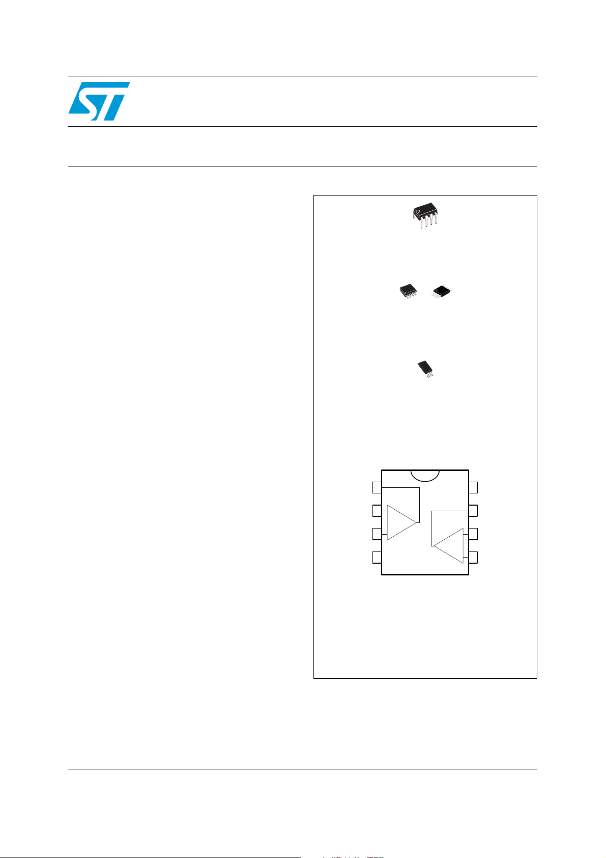
N
DIP-8
(Plastic package)
D & S
SO-8 & miniSO-8
(Plastic micropackage)
P
TSSOP8
(Thin shrink small outline package)
1
2
3
45
6
7
8
-
+
-
+
1 - Output 1
2 - Inverting input
3 - Non-inverting input
4 - V
CC
-
5 - Non-inverting input 2
6 - Inverting input 2
7 - Output 2
8 - V
CC
+
Pin connections
(top view)
Features
■ ESD internal protection: 2 kV
■ Internally frequency-compensated
■ Large DC voltage gain: 100 dB
■ Wide bandwidth (unity gain): 1.1 MHz
(temperature compensated)
■ Very low supply current per operator
essentially independent of supply voltage
■ Low input bias current: 20 nA (temperature
compensated)
■ Low input offset voltage: 2 mV
■ Low input offset current: 2 nA
■ Input common-mode voltage range includes
ground
■ Differential input voltage range equal to the
■ Large output voltage swing 0 V to V
power supply voltage
CC
+
-1.5V
LM158W-LM258W-LM358W
Datasheet − production data
Description
These circuits consist of two independent, highgain, internally frequency-compensated op-amps,
which are specifically designed to operate from a
single power supply over a wide range of
voltages. The low-power supply drain is
independent of the magnitude of the power supply
voltage.
Application areas include transducer amplifiers,
DC gain blocks and all the conventional op-amp
circuits, which can now be more easily
implemented in single power supply systems. For
example, these circuits can be directly supplied
with the standard +5 V, which is used in logic
systems and will easily provide the required
interface electronics with no additional power
supply.
In linear mode the input common-mode voltage
range includes ground and the outputvoltage can
July 2012 Doc ID 9159 Rev 9 1/20
This is information on a product in full production.
also swing to ground, even though operated from
only a single power supply voltage.
www.st.com
20

Contents LM158W-LM258W-LM358W
Contents
1 Schematic diagram . . . . . . . . . . . . . . . . . . . . . . . . . . . . . . . . . . . . . . . . . . 3
2 Absolute maximum ratings and operating conditions . . . . . . . . . . . . . 4
3 Electrical characteristics . . . . . . . . . . . . . . . . . . . . . . . . . . . . . . . . . . . . . 6
4 Typical applications . . . . . . . . . . . . . . . . . . . . . . . . . . . . . . . . . . . . . . . . 11
5 Package information . . . . . . . . . . . . . . . . . . . . . . . . . . . . . . . . . . . . . . . . 13
5.1 DIP8 package information . . . . . . . . . . . . . . . . . . . . . . . . . . . . . . . . . . . . 14
5.2 SO-8 package information . . . . . . . . . . . . . . . . . . . . . . . . . . . . . . . . . . . . 15
5.3 MiniSO-8 package information . . . . . . . . . . . . . . . . . . . . . . . . . . . . . . . . . 16
5.4 TSSOP8 package information . . . . . . . . . . . . . . . . . . . . . . . . . . . . . . . . . 17
6 Ordering information . . . . . . . . . . . . . . . . . . . . . . . . . . . . . . . . . . . . . . . 18
7 Revision history . . . . . . . . . . . . . . . . . . . . . . . . . . . . . . . . . . . . . . . . . . . 19
2/20 Doc ID 9159 Rev 9
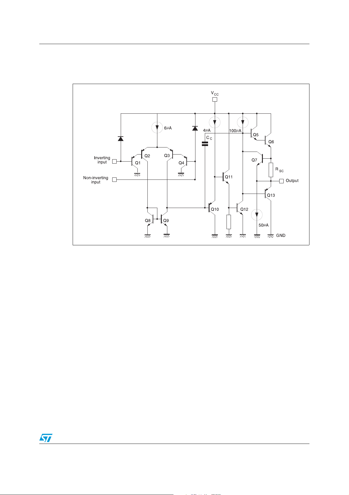
LM158W-LM258W-LM358W Schematic diagram
1 Schematic diagram
Figure 1. Schematic diagram (1/2 LM158W)
Doc ID 9159 Rev 9 3/20
Absolute maximum ratings and operating conditions LM158W-LM258W-LM358W
2 Absolute maximum ratings and operating conditions
Table 1. Absolute maximum ratings
Symbol Parameter LM158W/AW LM258W/AW LM358W/AW Unit
+
V
CC
V
V
I
T
oper
T
R
R
ESD
Supply voltage +32 V
Input voltage -0.3 to V
in
Differential input voltage -0.3 to V
id
Output short-circuit duration
Input current
in
(2)
(1)
5mA in DC or 50mA in AC (duty cycle=10%,
+0.3 V
CC+
+0.3 V
CC+
Infinite
T=1s)
Operating free-air temperature range -55 to +125 -40 to +105 0 to +70 °C
Storage temperature range -65 to +150 °C
stg
T
Maximum junction temperature 150 °C
j
(3)
(3)
125
190
120
85
40
39
37
41
2kV
200 V
1.5 kV
Thermal resistance junction to ambient
SO-8
thja
MiniSO-8
TSSOP8
DIP-8
Thermal resistance junction to case
SO-8
thjc
MiniSO-8
TSSOP8
DIP-8
HBM: human body model
MM: machine model
(5)
CDM: charged device model
(4)
(6)
mA
°C/W
°C/W
1. Short-circuits from the output to VCC can cause excessive heating if VCC > 15 V. The maximum output current is
approximately 40 mA independent of the magnitude of V
circuits on all amplifiers.
2. This input current only exists when the voltage at any of the input leads is driven negative. It is due to the collector-base
junction of the input PNP transistor becoming forward biased and thereby acting as input diode clamps. In addition to this
diode action, there is also NPN parasitic action on the IC chip. This transistor action can cause the output voltages of the
Op-amps to go to the V
negative. This is not destructive and normal output will be restored for input voltage higher than -0.3 V.
3. Short-circuits can cause excessive heating and destructive dissipation. R
4. Human body model: a 100 pF capacitor is discharged through a 1.5 kΩ resistor between two pins of the device, done for all
couples of pin combinations with other pins floating.
5. Machine model: a 200 pF capacitor is charged to the specified voltage, then discharged directly between two pins of the
device with no external series resistor (internal resistor < 5 Ω), done for all couples of pin combinations with other pins
floating.
6. Charged device model: all pins plus package are charged together to the specified voltage and then discharged directly to
the ground.
voltage level (or to ground for a large overdrive) for the time during which an input is driven
CC
. Destructive dissipation can result from simultaneous short-
CC
are typical values.
th
4/20 Doc ID 9159 Rev 9
LM158W-LM258W-LM358W Absolute maximum ratings and operating conditions
Table 2. Operating conditions
Symbol Parameter Value Unit
+
V
V
T
1. When used in comparator, the functionality is guaranteed as long as at least one input remains within the
Supply voltage 3 to 30 V
CC
Common mode input voltage range
icm
(1)
V
-0.3 to VCC -1.5 V
DD
Operating free air temperature range
oper
LM158W
LM258W
LM358W
operating common mode voltage range.
-55 to +125
-40 to +105
0 to +70
°C
Doc ID 9159 Rev 9 5/20
Electrical characteristics LM158W-LM258W-LM358W
3 Electrical characteristics
Table 3. V
+
= +5 V, V
CC
(unless otherwise specified)
Symbol Parameter Min. Typ. Max. Unit
-
= ground, Vo = 1.4 V, T
CC
= +25°C
amb
V
DV
DI
max
(1)
1
1
2
2
2
3
5
7
mV
4
7
9
Input offset voltage
LM158AW
LM258AW, LM358AW
LM158W, LM258W
io
LM358W
T
min
LM158AW, LM258AW, LM358AW
LM158W, LM258W
LM358W
≤ T
amb
≤ T
Input offset voltage drift
io
LM158AW, LM258AW, LM358AW
LM158W, LM258W, LM358W
7
7
15
30
µV/°C
Input offset current
LM158AW, LM258AW, LM358AW
I
io
LM158W, LM258W, LM358W
≤ T
T
min
amb
≤ T
max
2
2
LM158AW, LM258AW, LM358AW
LM158W, LM258W, LM358W
10
30
30
40
nA
Input offset current drift
io
LM158AW, LM258AW, LM358AW
LM158W, LM258W, LM358W
Input bias current
(2)
LM158AW, LM258AW, LM358AW
I
ib
LM158W, LM258W, LM358W
≤ T
T
min
amb
≤ T
max
LM158AW, LM258AW, LM358AW
LM158W, LM258W, LM358W
10
10
20
20
200
300
50
150
100
200
pA/°C
nA
Large signal voltage gain
A
vd
+
= +15 V, RL = 2 kΩ, Vo = 1.4 V to 11.4 V
V
CC
T
≤ T
amb
≤ T
max
min
Supply voltage rejection ratio
amb
CC
≤ T
+
= 5 V to 30 V
max
SVR
≤10 kΩ, V
R
s
T
min
≤ T
Supply current, all amp, no load
I
CC
T
≤ T
≤ T
amb
amb
≤ T
≤ T
max
max
min
T
min
, V
, V
CC
CC
+
+
= +5 V
= +30 V
6/20 Doc ID 9159 Rev 9
50
25
65
65
100 V/mV
100 dB
0.7 1.2
mA
2
 Loading...