

Three terminal adjustable current sources
Features
■ Operates from 1V to 40V
■ 0.02%/V current regulation
■ Programmable from 1µA to 10mA
■ ±3% initial accuracy
Description
The LM134/LM234/LM334 are 3-terminal
adjustable current sources characterized by:
■ an operating current range of 10000: 1
■ an excellent current regulation
■ a wide dynamic voltage range of 1V t 10V
The current is determined by an external resistor
without requiring other external components.
Reverse voltages of up to 20V will only draw a
current of several microamperes. This enables the
circuit to operate as a rectifier and as a source of
current in a.c. applications.
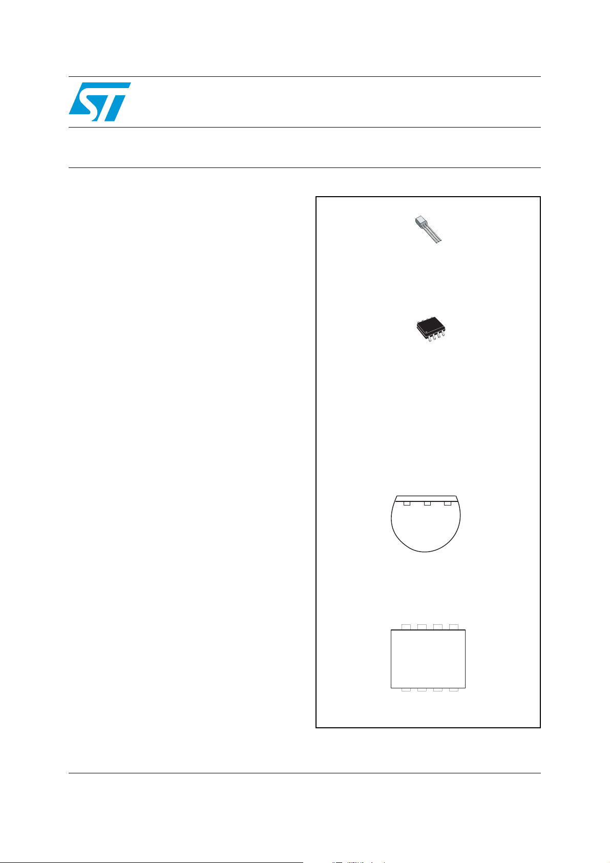
LM134-LM234-LM334
Z
TO-92
(Plastic package)
D
SO-8
(Plastic micropackage)
Pin connections
TO-92
(Bottom view)
For the LM134/LM234/LM334, the voltage on the
control pin is 64mV at +25°C and is directly
ADJ
v+
21
v-
3
proportional to the absolute temperature (°K). T he
simplest external resistor connection generates a
current with approxima tely 0. 33%/°C te mper ature
dependence. Zero drift can be obtained by adding
an additional resistor and a diode to the e xternal
circuit.
SO-8
(Top view)
NC NC
8765
1234
ADJ
NC
May 2007 Rev 3 1/16
NC
V-
NC
V+
www.st.com
16
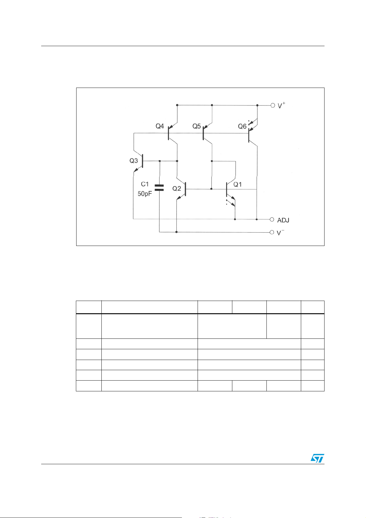
Schematic diagram LM134-LM234-LM334
1 Schematic diagram
Figure 1. Schematic diagram
2 Absolute maximum ratings
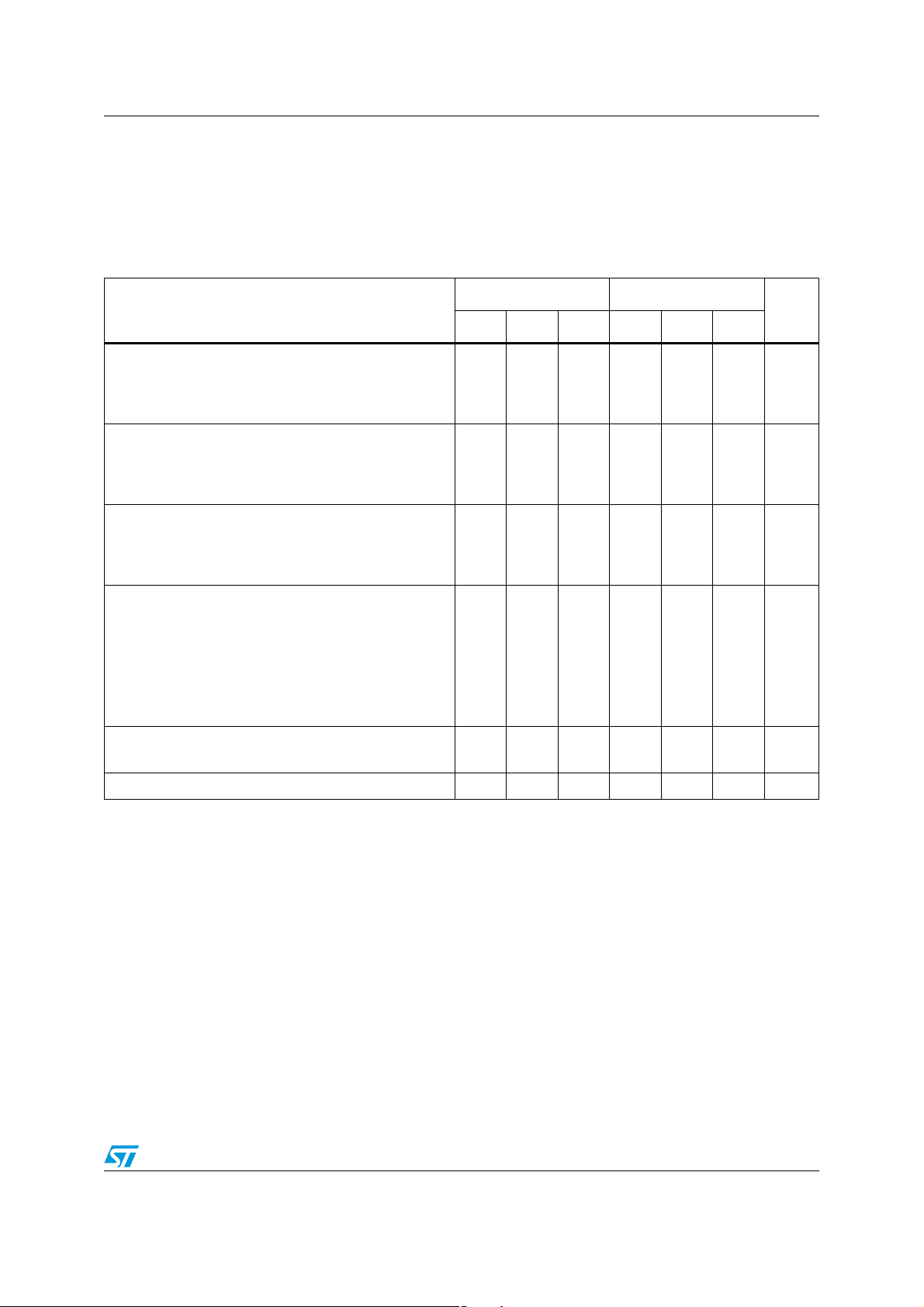
Table 1. Absolute maximum ratings
Symbol Parameter LM134 LM234 LM334 Unit
Voltage V+ to V-
Forward
Reverse
-
V
P
T
T
ADJ pin to V- voltage 5 V
ADJ
I
Set current 10 mA
set
Power dissipation 400 mW
tot
Storage temperature range -65 to +150 °C
stg
Operating free-air temperature range -55 to +125 -25 to +100 0 to +70 °C
oper
40
20
30
20
V
2/16
LM134-LM234-LM334 Electrical characteristics
3 Electrical characteristics
Tj = +25°C with pulse testing so that junction temperature does not change during testing
(unless otherwise specified)
Table 2. Electrical characteristics
Set current error (V+ = +2.5V) -
10µA ≤ I
1mA ≤ I
2µA ≤ I
Ratio of set current to V
10µA ≤ I
1mA ≤ I
2µA ≤ I
Minimum operating voltage
2µA ≤ I
100µA ≤ I
1mA ≤ I
Average change in set current with input voltage
2µA ≤ I
+1.5V ≤ V
+5V ≤ V+ ≤ +40V
1mA ≤ I
+1.5V ≤ V+ ≤ +5V
+5V ≤ V
Temperature dependence of set current 25µA ≤ I
Effective shunt capacitance 15 15 pF
1. The set current is the current flowing into the V+ pin. It is determined by the following formula:
= 67.7mV/R
I
set
The set current error is expressed as a percent deviation from this amount.
is directly proportional to absolute temperature (°K). I
2. I
set
= Io (T/To)
I
set
where I
LM134 - LM234 LM334
Parameter
Min. Typ. Max. Min. Typ. Max.
(1)
≤ 1mA
set
≤ 5mA
set
≤ 10µA
set
current
-
14 18
14
14
0.8
0.9
1
0.02
set
set
set
set
≤ 1mA
set
≤ 1mA
set
≤ 5mA
≤ 10µA
≤ 100µA
≤ 1mA
set
≤ 5mA
+
≤ +5V
0.01
≤ 5mA
set
+
≤ +40V
(2)
≤ 1mA 0.96 T T 1.04 T 0.96 T T 1.04 T
set
(Tj = +25°C)
set
at any temperature can be calculated from
set
is I
measured at To (°K).
o
set
0.03
0.02
3
5
8
23 14 18
0.05
0.03
14
14
0.8
0.9
1
0.02
0.01
0.03
0.02
Unit
6
8
%
12
26
V
0.1
0.05 % / V
3/16
Electrical characteristics LM134-LM234-LM334
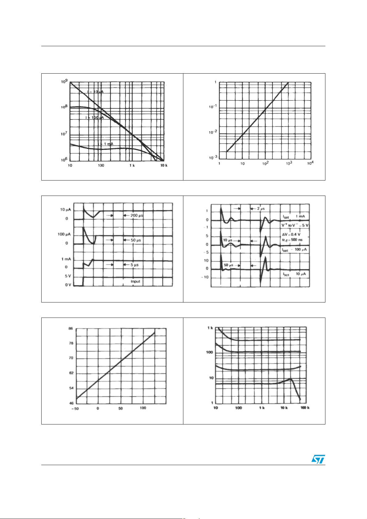
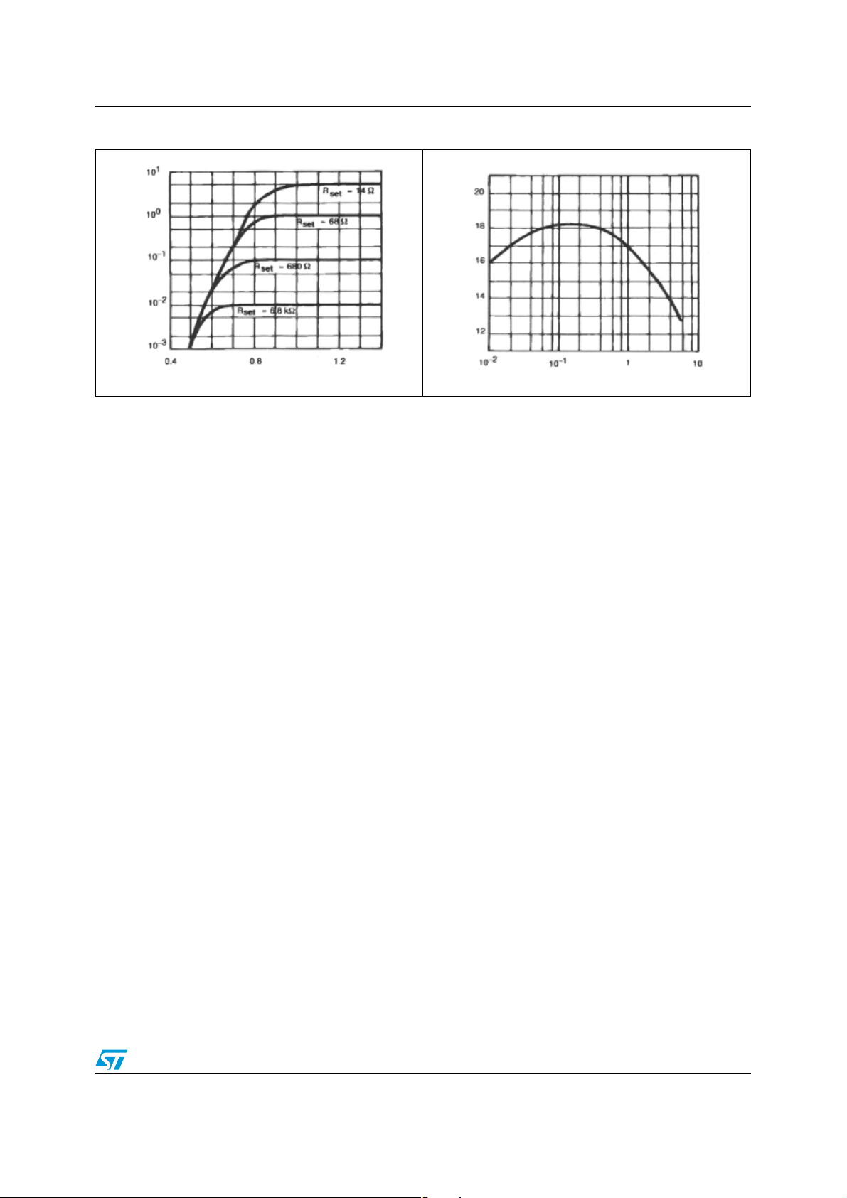
Figure 2. Output impedance Figure 3. Maximum slew rate for linear
operation
Impedance (Ohm)
Frequency (Hz)
Slew rate (V/µs)
I
set
(µA)
Figure 4. Startup Figure 5. Transient response
Time (scale changes at each current level) Time (scale changes at each current level)
Figure 6. Voltage across R
set
Figure 7. Current noise
Voltage (mV)
Current (pA/√Hz)
Temperature (°C)
4/16
Frequency (Hz)
LM134-LM234-LM334 Electrical characteristics
Figure 8. Turn-on voltage Figure 9. Ratio of I
(mA)
I
set
Ratio
V+ to V- voltage (V)
to V- current
set
I
(mA)
set
5/16

Application information LM134-LM234-LM334
4 Application information
4.1 Slew rate
At slew rates abo v e a threshold (see Figure 4 and Figure 5), the LM134, LM234, LM334 can
have a non-linear current characteristic. The slew rate at which this takes place is directly
proportional to I
Slew rates of more than 1V/µs do not dama ge the circuit nor do they produce high currents.
4.2 Thermal effects
set
. At I
= 10µA, dv/dt max. = 0.01V/µs ; at I
set
= 1mA, dv/dt max. = 1V/µs.
set
Internal heating can have a significant effect on current regulation for an I
For ex ample, each increase of 1V in the voltage across the LM134 at I
increase the junction temperature by ≈ 0.4°C (in still air). The output current (I
temperature coefficient of about 0.33%/°C. Thus the change in current due to the increase
in temperature will be (0.4) (0.33) = 0.132%. This is a degradation of 10 : 1 in regulation
versus the true electrical eff ects. Thermal effects should be taken into account when d.c.
regulation is critical and I
set
4.3 Shunt capacitance
In certain applications, the 15pF value for the shunt capacitance should be reduced:
● because of loading problems,
● because of limitation of output impedance of the current source in a.c. applications.
You can easily reduce the capacitan ce by adding a FET as shown in Typical applications on
page 8.
The value of this capacitance can be reduced by at least 3pF and regulation can be
improved by an order of magnitude without any modifications of the d.c. characteristics
(except for the minimum input voltage).
4.4 Noise
is higher than 100µA.
above 100µA.
set
= 1mA will
set
) has a
set
The current noise produced by LM134, LM234, and LM334 is about 4 times that of a
transistor. If the LM134, LM234, LM334 is used as an active load for a transistor amplifier,
the noise at the input will increase by about 12dB. In most cases this is acceptable, and a
single amplifier can be built with a voltage gain higher than 2000.
4.5 Lead resistance
The sense voltage which determines the current of the LM134, LM234, LM334 is less than
100mV. At this level, the thermocouple effects and the connection resistan ce should be
reduced by locating the current setting resistor close to the device. Do not use sockets for
the ICs. A contact resistance of 0.7Ω is sufficient to decrease the output current by 1% at the
1mA level.
6/16

LM134-LM234-LM334 Application information
4.6 Sensing temperature
The LM134, LM234, LM334 are excellent remote controlled temperature sensors because
their operation as current sources preserves their accuracy even in the case of long
connecting wires. The output current is directly proportional to the absolute temperature in
Kelvin degrees acco rding to the following equation.
227µV/°K) (T()
---------------------------------------- -
I
=
set
The calibration of the LM134, LM234, LM334 is simplified by the fact that most of the initial
accuracy is due to gain limitation (slope error) and not an offset. Gain adjustment is a one
point trim because the output of the device extrapolates to zero at 0°K.
Figure 10. Device calibration
R
set
This particularity of the LM134, LM234, LM334 is illustrated in the above diagram. Line abc
represents the sensor current before adjustment and line a’b’c’ represents the desired
output. A gain adjustment provided at T2 will move the output from b to b’ and will correct
the slope at the same time so that the output at T1 and T3 will be correct. This gain
adjustment can be carried out by means of R
adjustment, the slope error should be less than 1%. A low temper ature coeff icient f o r R
necessary to keep this accuracy. A 33ppm/°C temperature drift of R
or the load resistor used in the circuit. After
set
will give an error of
set
set
is
1% on the slope because the resistance follows the same temperature variations as the
LM134, LM234, LM334.
Three wires are required to isolate R
from the LM134, LM234, LM334. Since this solut ion
set
is not recommended, metal-film resistors with a drift of less than 20ppm/°C are now
available. Wirewound resistors can be used when very high stability is required.
7/16

Application information LM134-LM234-LM334
Typical applications
Figure 11. Basic 2-terminal current source Figure 12. Alternate trimming technique
Figure 13. Terminating remote sensor for
voltag e ou tput
Figure 14. Zero temperature coefficient
current source
8/16

LM134-LM234-LM334 Application information
Figure 15. Low output impedance
thermometer
Figure 16. Low output impedance
thermometer
Figure 17. Micropower bia s Figure 18. Low input voltage reference driver
9/16

Application information LM134-LM234-LM334
Figure 19. In-line current limiter Figure 20. Fet cascading for low capa citance
10/16

LM134-LM234-LM334 Package information
5 Package information
In order to meet environmental requirements, STMicroelectronics offers these devices in
ECOPACK
category of second level interconnect is marke d on the pa ckage and on the inner box label,
in compliance with JEDEC Standard JESD97. The maximum ratings related t o soldering
conditions are also marked on the inner box label. ECOPACK is an STMicroelectronics
trademark. ECOPACK specifications are available at: www.st.com
®
packages. These packages have a lead-free second level interconnect. The
.
11/16

Package information LM134-LM234-LM334
5.1 SO-8 package mechanical data
Dimensions
Ref.
Millimeters Inches
Min. Typ. Max. Min. Typ. Max.
A1.750.069
A1 0.10 0.25 0.004 0.010
A2 1.25 0.049
b 0.28 0.48 0.011 0.019
c 0.17 0.23 0.007 0.010
D 4.80 4.90 5.00 0.189 0.193 0.197
H 5.80 6.00 6.20 0.228 0.236 0.244
E1 3.80 3.90 4.00 0.150 0.154 0.157
e 1.27 0.050
h 0.25 0.50 0.010 0.020
L 0.40 1.27 0.016 0.050
k1°8°1°8°
ccc 0.10 0.004
12/16

LM134-LM234-LM334 Package information
5.2 TO-92 ammopack and tape & reel package mechanical data
A1
P
d
P
A
T
H
H
H1
L1
D0
P2
I1
F1
F2
P0
W2
H0
W0
W1
W
Millimeters Inches
Dim.
Min. Typ. Max. Min. Typ. Max.
AL 5.0 0.197
A 5.0 0.197
T 4.0 0.157
d 0.45 0.018
I1 2.5 0.098
P 11.7 12.7 13.7 0.461 0.500 0.539
PO 12.4 12.7 13 0.488 0.500 0.512
P2 5.95 6.35 6.75 0.234 0.250 0.266
F1/F2 2.4 2.5 2.8 0.094 0.098 0.110
Δh -1 0 1 -0.039 0 0.039
ΔP -1 0 1 -0.039 0 0.039
W 17.5 18.0 19.0 0.689 0.709 0.748
W0 5.7 6 6.3 0.224 0.236 0.248
W1 8.5 9 9.75 0.335 0.354 0.384
W2 0.5 0.020
H200.787
H0 15.5 16 16.5 0.610 0.630 0.650
H1 25 0.984
DO 3.8 4.0 4.2 0.150 0.157 0.165
L1 11 0.433
13/16

Package information LM134-LM234-LM334
5.3 TO-92 bulk package mechanical data
Millimeters Inches
Dim.
Min. Typ. Max. Min. Typ. Max.
L 1.27 0.05
B 3.2 3.7 4.2 0.126 0.1457 0.1654
O1 4.45 5.00 5.2 0.1752 0.1969 0.2047
C 4.58 5.03 5.33 0.1803 0.198 0.2098
K12.7 0.5
O2 0.407 0.5 0.508 0.016 0.0197 0.02
a 0.35 0.0138
14/16

LM134-LM234-LM334 Ordering information
6 Ordering information
Table 3. Order codes
Part number
LM134D/DT -55°C to +125°C SO-8
LM134Z/ZT/AP -55°C to +125°C TO-92
LM234D/DT -25°C to +100°C SO-8
LM234Z/ZT/AP -24°C to +100°C TO-92
LM334D/DT -0°C to +70°C SO-8
LM334Z/ZT/AP -0°C to +70°C TO-92
LM334AD/ADT -0°C to +70°C SO-8
LM334AZ/AZT/AAP -0°C to +70°C TO-92
Temperature
range
Package Packing Marking
Tube or
Tape & reel
Bulk or
Tape & reel or
Ammopack
Tube or
Tape & reel
Bulk or
Tape & reel or
Ammopack
Tube or
Tape & reel
Bulk or
Tape & reel or
Ammopack
Tube or
Tape & reel
Bulk or
Tape & reel or
Ammopack
LM134
LM134
LM234
LM234
LM334
LM334
LM334A
LM334A
7 Revision history
Date Revision Changes
2-May-2003 1 Initial release.
28-Oct-2005 2 Internal revision.
29-May-2007 3
Corrected error in pinout diagram for TO-92 package on cover page
(it is a bottom view, not a top view).
Updated Section 5: Package information and expanded Table 3:
Order codes.
15/16

LM134-LM234-LM334
Please Read Carefully:
Information in this document is provided solely in connection with ST products. STMicroelectronics NV and its subsidiaries (“ST”) reserve the
right to make changes, corrections, modifications or improvements, to this document, and the products and services described herein at any
time, without notice.
All ST products are sold pursuant to ST’s terms and conditions of sale.
Purchasers are solely res ponsibl e fo r the c hoic e, se lecti on an d use o f the S T prod ucts and s ervi ces d escr ibed he rein , and ST as sumes no
liability whatsoever relati ng to the choice, selection or use of the ST products and services described herein.
No license, express or implied, by estoppel or otherwise, to any intellectual property rights is granted under this document. If any part of this
document refers to any third pa rty p ro duc ts or se rv ices it sh all n ot be deem ed a lice ns e gr ant by ST fo r t he use of su ch thi r d party products
or services, or any intellectua l property c ontained the rein or consi dered as a warr anty coverin g the use in any manner whats oever of suc h
third party products or servi ces or any intellectual propert y contained therein.
UNLESS OTHERWISE SET FORTH IN ST’S TERMS AND CONDITIONS OF SALE ST DISCLAIMS ANY EXPRESS OR IMPLIED
WARRANTY WITH RESPECT TO THE USE AND/OR SALE OF ST PRODUCTS INCLUDING WITHOUT LIMITATION IMPLIED
WARRANTIES OF MERCHANTABILITY, FITNESS FOR A PARTICUL AR PURPOS E (AND THEIR EQUIVALE NTS UNDER THE LAWS
OF ANY JURISDICTION), OR INFRINGEMENT OF ANY PATENT, COPYRIGHT OR OTHER INTELLECTUAL PROPERTY RIGHT.
UNLESS EXPRESSLY APPROVED IN WRITING BY AN AUTHORIZED ST REPRESENTATIVE, ST PRODUCTS ARE NOT
RECOMMENDED, AUTHORIZED OR WARRANTED FOR USE IN MILITARY, AIR CRAFT, SPACE, LIFE SAVING, OR LIFE SUSTAINING
APPLICATIONS, NOR IN PRODUCTS OR SYSTEMS WHERE FAILURE OR MALFUNCTION MAY RESULT IN PERSONAL INJ URY,
DEATH, OR SEVERE PROPERTY OR ENVIRONMENTAL DAMAGE. ST PRODUCTS WHICH ARE NOT SPECIFIED AS "AUTOMOTIVE
GRADE" MAY ONLY BE USED IN AUTOMOTIVE APPLICATIONS AT USER’S OWN RISK.
Resale of ST products with provisions different from the statements and/or technical features set forth in this document shall immediately void
any warranty granted by ST fo r the ST pro duct or serv ice describe d herein and shall not cr eate or exten d in any manne r whatsoever , any
liability of ST.
ST and the ST logo are trademarks or registered trademarks of ST in vari ous countries.
Information in this document su persedes and replaces all information previously supplied.
The ST logo is a registered trademark of STMicroelectronics. All other names are the property of their respective owners.
© 2007 STMicroelectronics - All rights reserved
STMicroelectronics group of compan ie s
Australia - Belgium - Brazil - Canada - China - Czech Republic - Finland - Fran ce - Germany - Hong Kong - India - Israel - Italy - Japan -
Malaysia - Malta - Morocco - Singapore - Spain - Sweden - Switzerland - United Kingdom - United States of America
www.st.com
16/16
 Loading...