

November1997
PROGR AMMABL E
QUAD BIPOLAR OPERAT ION AL AMPL IFI ERS
.PROGRAMMABLE ELECTRICAL CHARAC-
TERISTICS
.BATTERYPOWEREDOPERATION
.LOW SUPPLY CURRENT (250µA/amplifier)
.GAIN-BANDWIDTH PRODUCT: 1MHz
.LARGEDC VOLTAGEGAIN : 120dB
.LOW NOISEVOLTAGE: 28nV/VHz
.WIDE POWERSUPPLYRANGE:
±1.5Vto
±22V
.CLASSE AB OUTPUT STAGE. NO CROSS-
OVERDISTORTION
.OVERLOADPROTECTION FOR INPUTS AND
OUTPUTS
DESC RIP TI ON
The LM346consistsof fourindependent,highgain,
internallycompensated,low power programmable
amplifiers. Two external resistors (R
set
) allow the
user to program the gain-bandwith product, slew
rate,supply current,inputbias current,input offset
currentand input noise. For example the user can
trade-off supply current for bandwidth or optimize
noisefigurefora givensource resistance.In a similar wayother amplifiercharacteristicscanbe
tailoredto theapplication.
Exceptfor thetwo programming pins at the end of
the packagethe LM346pin out is the sameas the
LM324and LM348.
PROGRAMMINGEQUATIONS:
Totalsupplycurrent= 1mA(I
set
=10µA)
Gain-bandwidthproduct = 1MHz (I
set
=10µA)
Slewrate = 0.5V/µs(I
set
=10µA)
Inputbias current ≈30 nA (I
set
=10µA)
I
set
=currentinto pin8 and pin 9
(see schematicdiagram)
I
set
=
V
CC
+
− V
CC
−
− 0.6V
R
set
4
5
6
7
9
10
11
12
13
15
1
2
3
8
16
14
Output1
Invertinginput 1
Non-invertinginput1
Non-invertinginput 2
Invertinginput 2
Output2
Set
Output4
Invertinginput 4
Non-invertinginput 4
V
CC
Non-invertinginput 3
Invertinginput 3
Output3
Set
V
CC
+
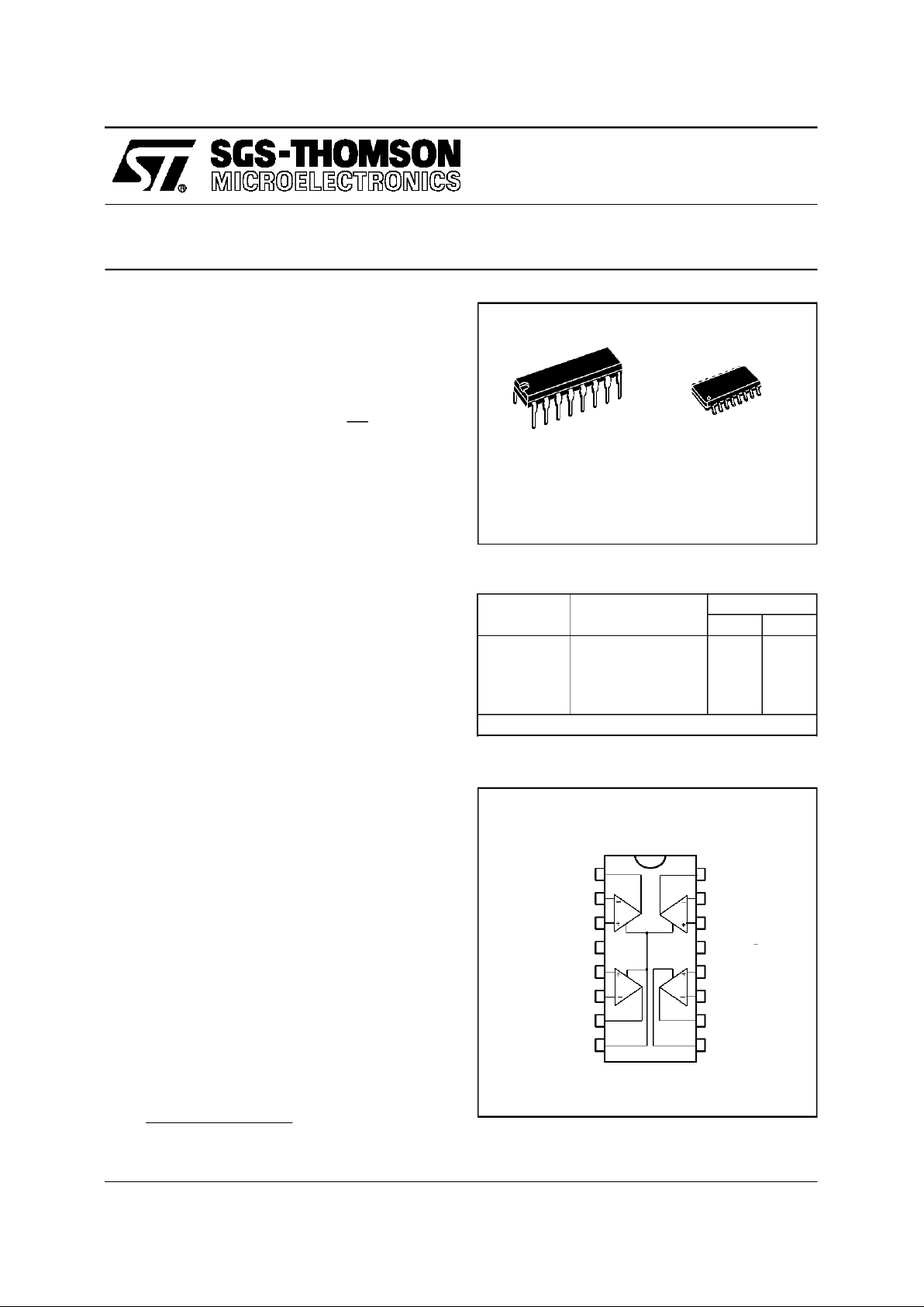
PIN C O NNEC TIO NS (top view)
ORDER CODES
Part
Number
Temperature
Range
Package
ND
LM146 –55
o
C, +125oC ••
LM246 –40
o
C, +105oC ••
LM346 0
o
C, +70oC ••
Example : LM246N
N
DIP16
(PlasticPackage)
D
SO16
(PlasticMicropackage)
LM146
LM246 - LM346
1/9
Notes : 1. For supply volt ages less than ±15V, the absolute maxi mum i nput voltage is equal t o the s upply vol tage.
2. Any of the ampl ifier output s can be shorted t o g r ound indefi nitly ; howev e r m or e t han one should n ot be
simul t aneous l y shorted as the maximum junction temperat ur e wi ll be exceeded.
ABSOLUTE MAXIMUM RATINGS
Symbol Parameter LM146 LM246 LM346 Unit
V
CC
Supply Voltage ±22 ±22 ±22
V
V
i
Input Voltage - (note 1) ±15 ±15 ±15 V
V
id
Differential Input Voltage ±30 ±30 ±30 V
Output Short-circuit Duration - (note 2) Infinite
P
tot
Power Dissipation
N/D Suffix 500
mW
T
oper
Operating Free-air Temperature Range –55 to +125 –40 to +105 0 to +70
o
C
T
stg
Storage Temperature Range –65 to +150 –65 to +150 –65 to +150
o
C
V
CC
V
CC
V
CC
or
Q18 Q19
Toother op amps
V
CCVCC
Output
R
set
R
set
I
set
I
set
SET
SET
R1
30Ω
Q12
Q10
Q11
Q9
Q16
Q15
Q14
Q13
8pF
C
C
Non-
inverting
input
Q20
Q6
Q8
Q5
R2
1kΩ
Q7Q21
Q4
Q3
Q17
V
CC
V
CC
Q1 Q2
Inverting
input
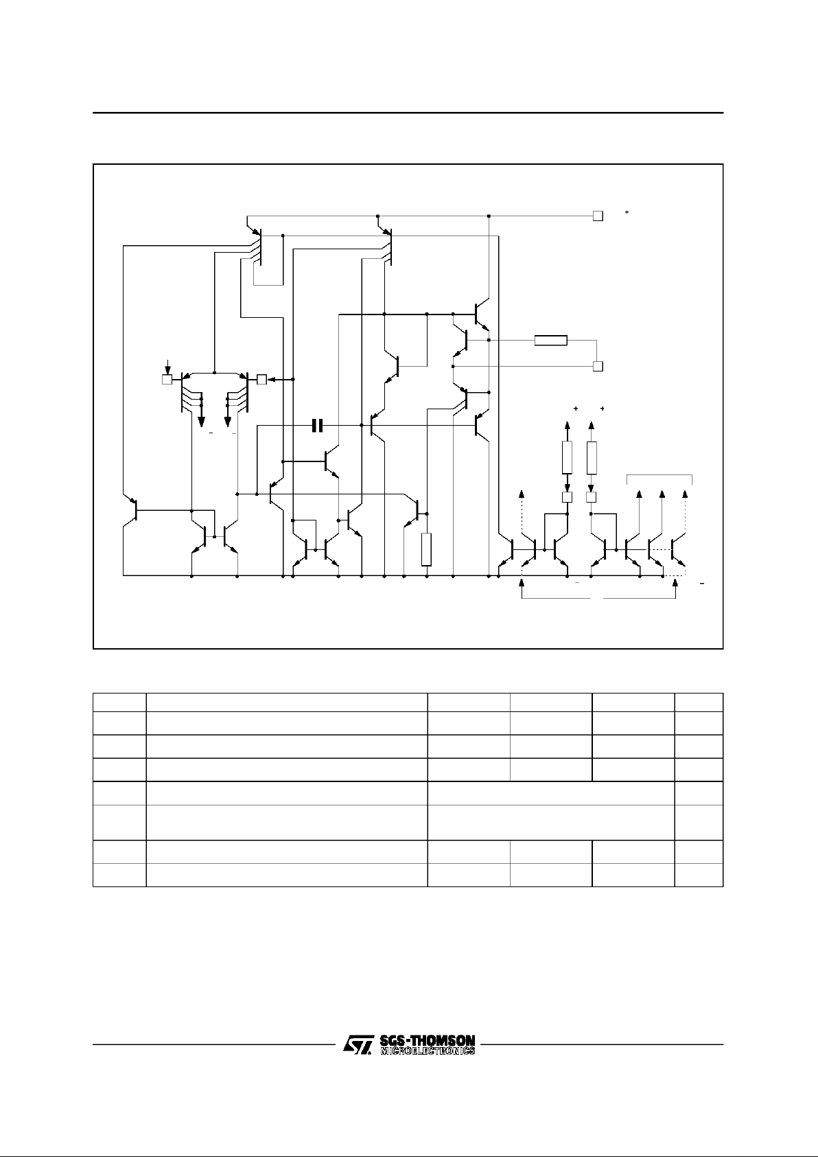
SCHE MATIC DIAGRAM ( 1/4 LM146)
LM146 - LM246 - LM346
2/9
ELECTRICAL CHARACTERISTICS
V
CC
= ±15V, I
set
=10µA, T
amb
= +25oC (unlessotherwise specified)
Symbol Parameter
LM146 LM246 - LM346
Unit
Min. Typ. Max. Min. Typ. Max.
V
io
Input Offset Voltage (RS≤ 10kΩ)
T
amb
=25oC
T
min
. ≤ T
amb
≤ T
max.
0.5 3
5
0.5 5
6
mV
I
io
Input Offset Current
T
amb
=25oC
T
min
. ≤ T
amb
≤ T
max.
220
25
2 100
100
nA
I
ib
Input Bias Current
T
amb
=25oC
T
min
. ≤ T
amb
≤ T
max.
30 100
100
30 250
250
nA
A
vd
Large Signal Voltage Gain
(V
o
= ±10V, RL= 10kΩ)
T
amb
=25oC
T
min
. ≤ T
amb
≤ T
max.
100501000 50251000
V/mV
SVR Supply Voltage Rejection Ratio (R
S
≤ 10kΩ)
T
amb
=25oC
T
min
. ≤ T
amb
≤ T
max.
8080110 8080110
dB
I
CC
Supply Current, all Amp, no Load
T
amb
=25oC
T
min
. ≤ T
amb
≤ T
max.
12
2
12
2
mA
V
icm
Input Common Mode Voltage Range
T
amb
=25oC
T
min
. ≤ T
amb
≤ T
max.
±13.5
±13.5
±13.5
±13.5
V
CMR Common Mode Rejection Ratio (R
S
≤ 10kΩ)
T
amb
=25oC
T
min
. ≤ T
amb
≤ T
max.
8070110 8070110
dB
I
OS
Output Short-circuit Current
T
amb
=25oC
T
min
. ≤ T
amb
≤ T
max.
10
4
20 30
35
10
4
20 30
35
mA
± V
opp
Output Voltage Swing (RL= 10kΩ)
T
amb
=25oC
T
min
. ≤ T
amb
≤ T
max.
12
12
14 12
12
14
V
SR Slew Rate (V
I
= ±10V, RL= 10kΩ,CL= 100pF,
unity Gain) 0.3 0.5 0.3 0.5
V/µs
R
I
Input Resistance 1 1 MΩ
C
I
Input Capacitance 2 2 pF
V
o1/Vo2
Channel Separation (RL= 10kΩ,Vo= 12Vpp) 120 120 dB
GBP Gain Bandwidth Product
(V
I
= 10 mV, RL= 10kΩ,CL= 100pF
f = 100kHz) 0.8 1 0.5 1
MHz
THD Total Harmonic Distortion
(f = 1kHz, A
v
= 20dB, RL= 10kΩ
C
L
= 100pF, vo=2Vpp) 0.015 0.015
%
e
n
Equivalent Input Noise Voltage
(f = 1kHz, R
s
= 100Ω)
28 28
nV
√Hz
LM146 - LM246 - LM346
3/9

LM146 - LM246 - LM346
4/9

LM146 - LM246 - LM346
5/9

LM146 - LM246 - LM346
6/9

50
0
-50
50
-50
0
INPUT (mV) OUTPUT (mV)
0
1
2345
TIME ( µs)
=10µAI
set
=+25°CT
amb
V
CC
=15V
= 10kΩ
R
L
= 100pF
C
L
VOLTAGE FO L LOWE R TRANSIENT
RESPONSE
1/4
LM146
G
e
I
C
L
L
R
TRANSIENT RESPONSE TEST CIRCUIT
LM146 - LM246 - LM346
7/9

PM-DIP16.EPS
PACKAGE MECHANICAL DATA
16 PINS - PLASTI C DI P
Dimensions
Millimeters Inches
Min. Typ. Max. Min. Typ. Max.
a1 0.51 0.020
B 0.77 1.65 0.030 0.065
b 0.5 0.020
b1 0.25 0.010
D 20 0.787
E 8.5 0.335
e 2.54 0.100
e3 17.78 0.700
F 7.1 0.280
i 5.1 0.201
L 3.3 0.130
Z 1.27 0.050
DIP16.TBL
LM146 - LM246 - LM346
8/9

PM-SO16.EPS
PACKAGE MECHANICAL DATA
16 PI NS - PLAS TI C MICROPA CKA G E (SO)
Dimensions
Millimeters Inches
Min. Typ. Max. Min. Typ. Max.
A 1.75 0.069
a1 0.1 0.2 0.004 0.008
a2 1.6 0.063
b 0.35 0.46 0.014 0.018
b1 0.19 0.25 0.007 0.010
C 0.5 0.020
c1 45
o
(typ.)
D 9.8 10 0.386 0.394
E 5.8 6.2 0.228 0.244
e 1.27 0.050
e3 8.89 0.350
F 3.8 4.0 0.150 0.157
G 4.6 5.3 0.181 0.209
SO16.TBL
Information furnished is believed to be accurate and reliable. However, SGS-THOMSON Microelectronics assumes no responsibility for the consequences of use of such information nor for any infringement of patents or other rights of third parties which
may result from its use. No license is granted by implication or otherwise under any patent or patent rights of SGS-THOMSON
Microelectronics. Specification mentioned in this publication are subject to change without notice. This publication supersedes
and replaces all information previously supplied. SGS-THOMSON Microelectronics products are not authorized for use as critical
components in life support devices or systems without express written approval of SGS-THOMSON Microelectronics.
1997 SGS-THOMSON Microelectronics – Printed in Italy – All Rights Reserved
SGS-THOMSON Microelectronics GROUP OF COMPANIES
Australia - Brazil - Canada - China - France - Germany - Hong Kong - Italy - Japan - Korea - Malaysia - Malta - Morocco
The Netherlands - Singapore - Spain - Sweden - Switzerland - Taiwan - Thailand - United Kingdom - U.S.A.
ORDERCODE :
LM146 - LM246 - LM346
9/9
 Loading...