

Very low dropout voltage regulators with inhibit function
Features
■ Very low dropout voltage (0.2 V typ.)
■ Very low quiescent current (typ. 50 µA in OFF
mode, 0.5 mA in ON mode, no load)
■ Output current up to 100 mA
■ Output voltages of 3 V, 3.3 V, 4.5 V, 5 V, 8 V
■ Internal current and thermal limit
■ Small 2.2 µF capacitor for stability
■ Available in ± 1% (A) or ± 2% (C) selection at
25 °C
■ Supply voltage rejection: 80 dB (typ.)
■ Temperature range: - 40 to 125 °C
Description
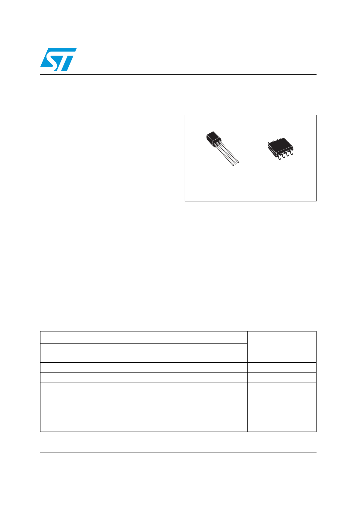
The LExxAB and LExxC are very low dropout
voltage regulators available in SO-8 and TO-92
packages and over a wide range of output
voltages.
The very low dropout voltage (0.2 V) and the very
low quiescent current make them particularly
suitable for low-noise low-power applications and
especially in battery-powered systems.
LExxAB
LExxC
Datasheet − production data
TO-92
These devices are pin-to-pin compatible with the
older L78Lxx series. Furthermore, in the 8-pin
configuration (SO-8) they employ a shutdown
logic control (pin 5, TTL compatible). This means
that when the device is used as a local regulator,
a part of the board can be put in standby,
decreasing even more total power consumption.
In the three-terminal configuration (TO-92) the
device is always in the ON state, maintaining the
same electrical performance. It requires only a
2.2 µF capacitor for stability, reducing component
size and cost.
SO-8
Table 1. Device summary
Order codes
SO-8
(tape and reel)
LE30CD-TR 3 V
LE33CD-TR LE33CZ-TR LE33CZ-AP 3.3 V
LE45CD-TR 4.5 V
LE50ABD-TR LE50ABZ-AP 5 V
LE50CD-TR 5 V
LE80CD-TR 8 V
May 2012 Doc ID 2573 Rev 13 1/22
This is information on a product in full production.
TO-92
(tape and reel)
LE30ABZ-TR 3 V
TO-92 (Ammopak)
Output voltages
www.st.com
22

Contents LExxAB, LExxC
Contents
1 Diagram . . . . . . . . . . . . . . . . . . . . . . . . . . . . . . . . . . . . . . . . . . . . . . . . . . . 3
2 Pin configuration . . . . . . . . . . . . . . . . . . . . . . . . . . . . . . . . . . . . . . . . . . . 4
3 Maximum ratings . . . . . . . . . . . . . . . . . . . . . . . . . . . . . . . . . . . . . . . . . . . . 5
4 Electrical characteristics . . . . . . . . . . . . . . . . . . . . . . . . . . . . . . . . . . . . . 6
5 Typical performance characteristics . . . . . . . . . . . . . . . . . . . . . . . . . . . 13
6 Package mechanical data . . . . . . . . . . . . . . . . . . . . . . . . . . . . . . . . . . . . 16
7 Revision history . . . . . . . . . . . . . . . . . . . . . . . . . . . . . . . . . . . . . . . . . . . 21
2/22 Doc ID 2573 Rev 13
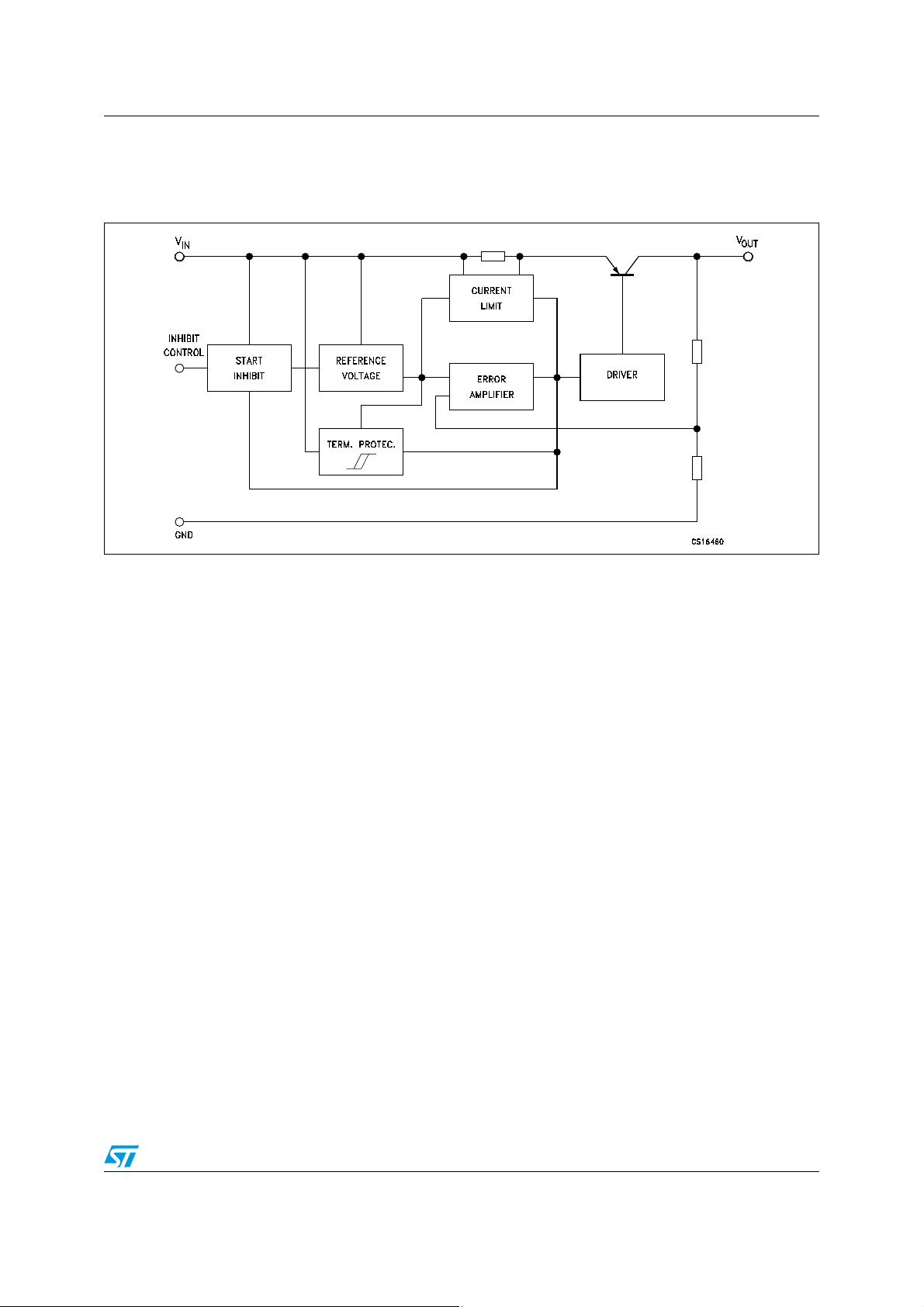
LExxAB, LExxC Diagram
1 Diagram
Figure 1. Block diagram
Doc ID 2573 Rev 13 3/22
Pin configuration LExxAB, LExxC
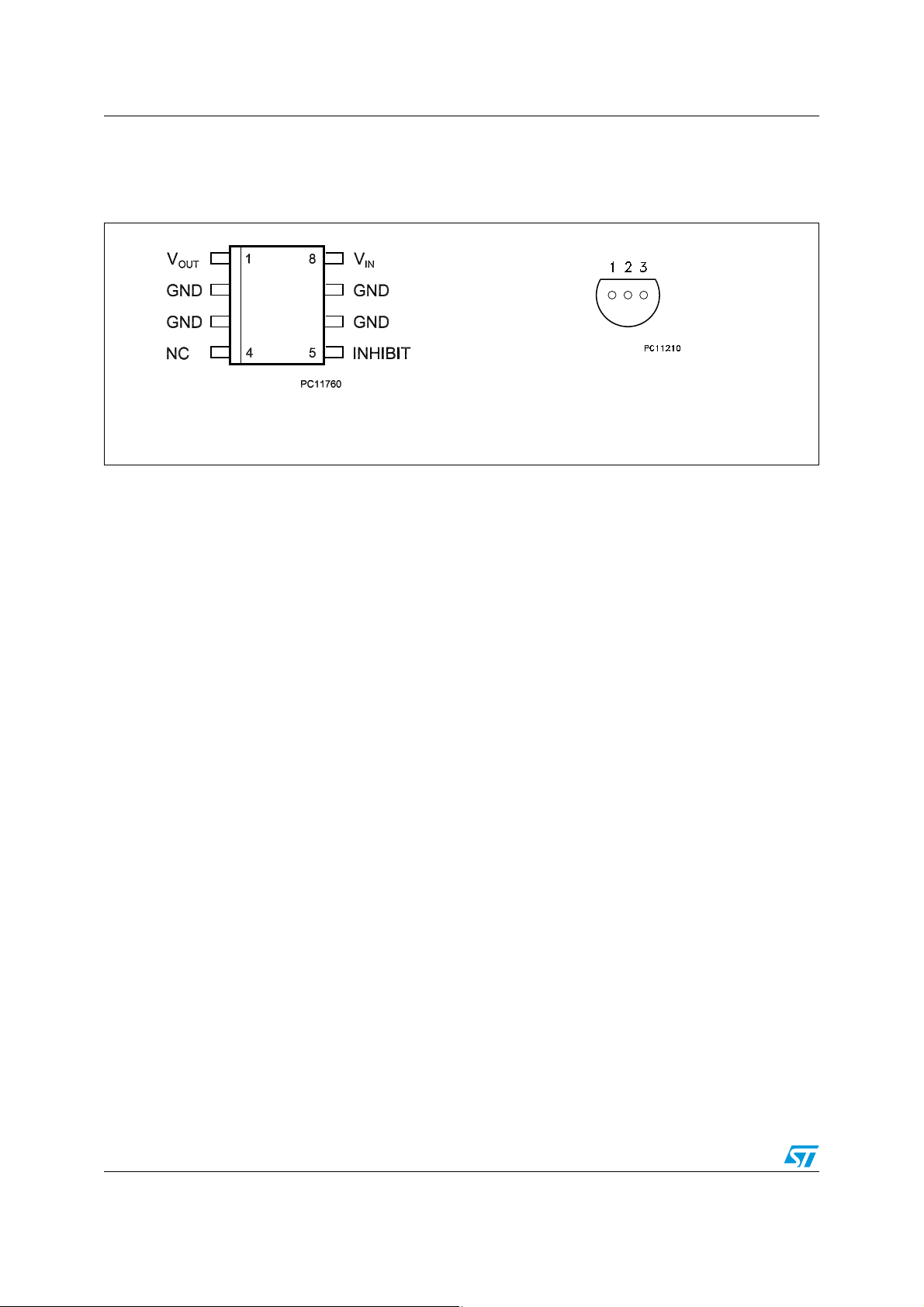
2 Pin configuration
Figure 2. Pin connections (top view for SO-8, bottom view for TO-92)
SO-8
PIN 1 = V
OUT
PIN 2 = GND
PIN 3 = V
IN
TO-92
4/22 Doc ID 2573 Rev 13
LExxAB, LExxC Maximum ratings
3 Maximum ratings
Table 2. Absolute maximum ratings
Symbol Parameter Value Unit
V
I
I
O
P
TOT
T
STG
T
OP
1. Our SO-8 package used for voltage regulators is modified internally to have pins 2, 3, 6 and 7 electrically fused to the die
attach pad. This particular frame decreases the total thermal resistance of the package and increases its ability to dissipate
power when an appropriate area of copper on the printed circuit board is available for heatsinking. The external dimensions
are the same as for the standard SO-8.
DC input voltage 20 V
Output current Internally limited
(1)
Power dissipation Internally limited
Storage temperature range -65 to 150 °C
Operating junction temperature range -40 to 125 °C
Table 3. Thermal data
Symbol Parameter SO-8 TO-92 Unit
R
thJC
R
thJA
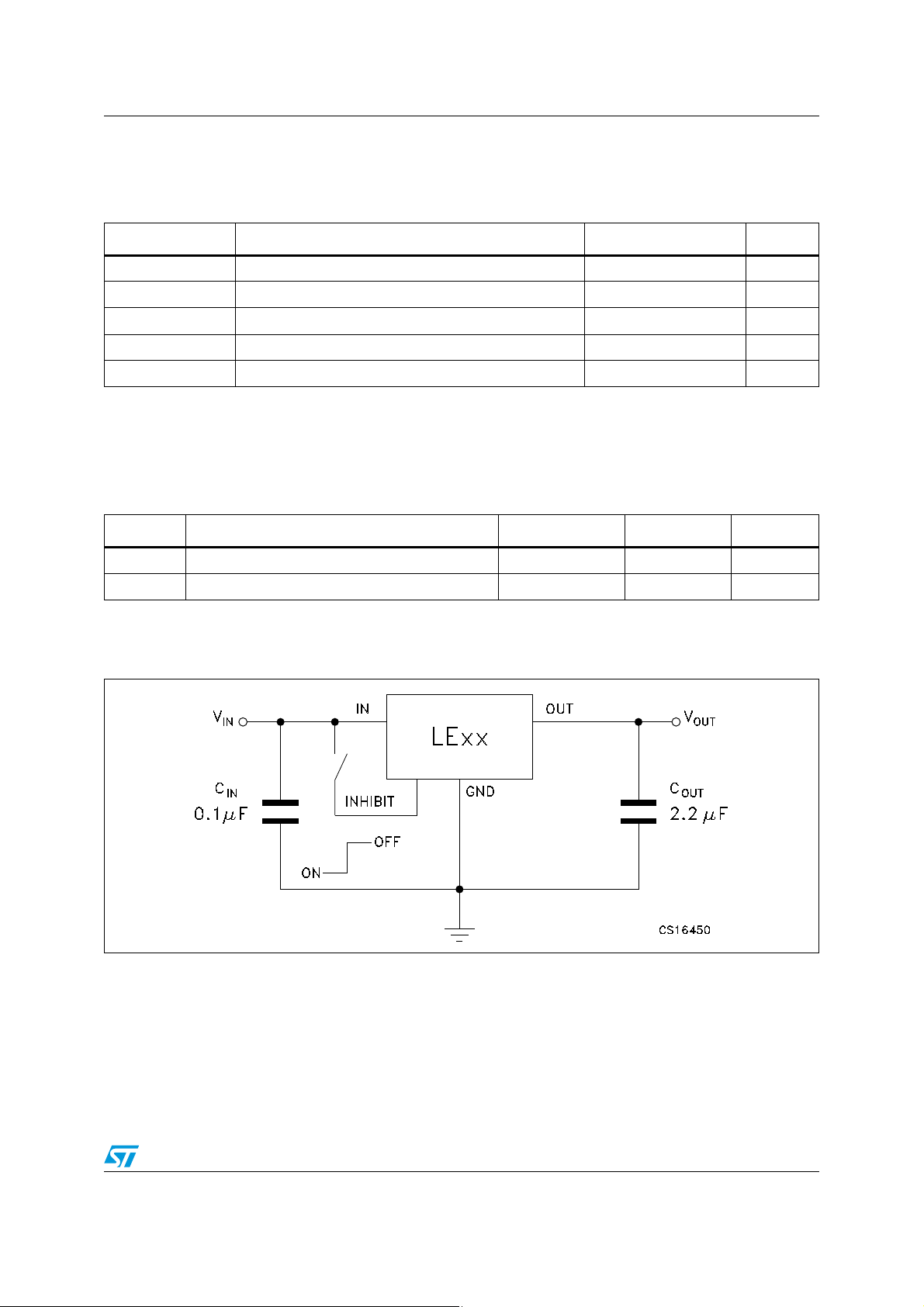
Figure 3. Test circuit
Thermal resistance junction-case 20 °C/W
Thermal resistance junction-ambient 55 200 °C/W
Note: If the INHIBIT pin is left floating, the regulator is in the ON mode. However, to avoid picking
up any noise, it is suggested to ground it when the Inhibit function is not used.
Doc ID 2573 Rev 13 5/22
Electrical characteristics LExxAB, LExxC
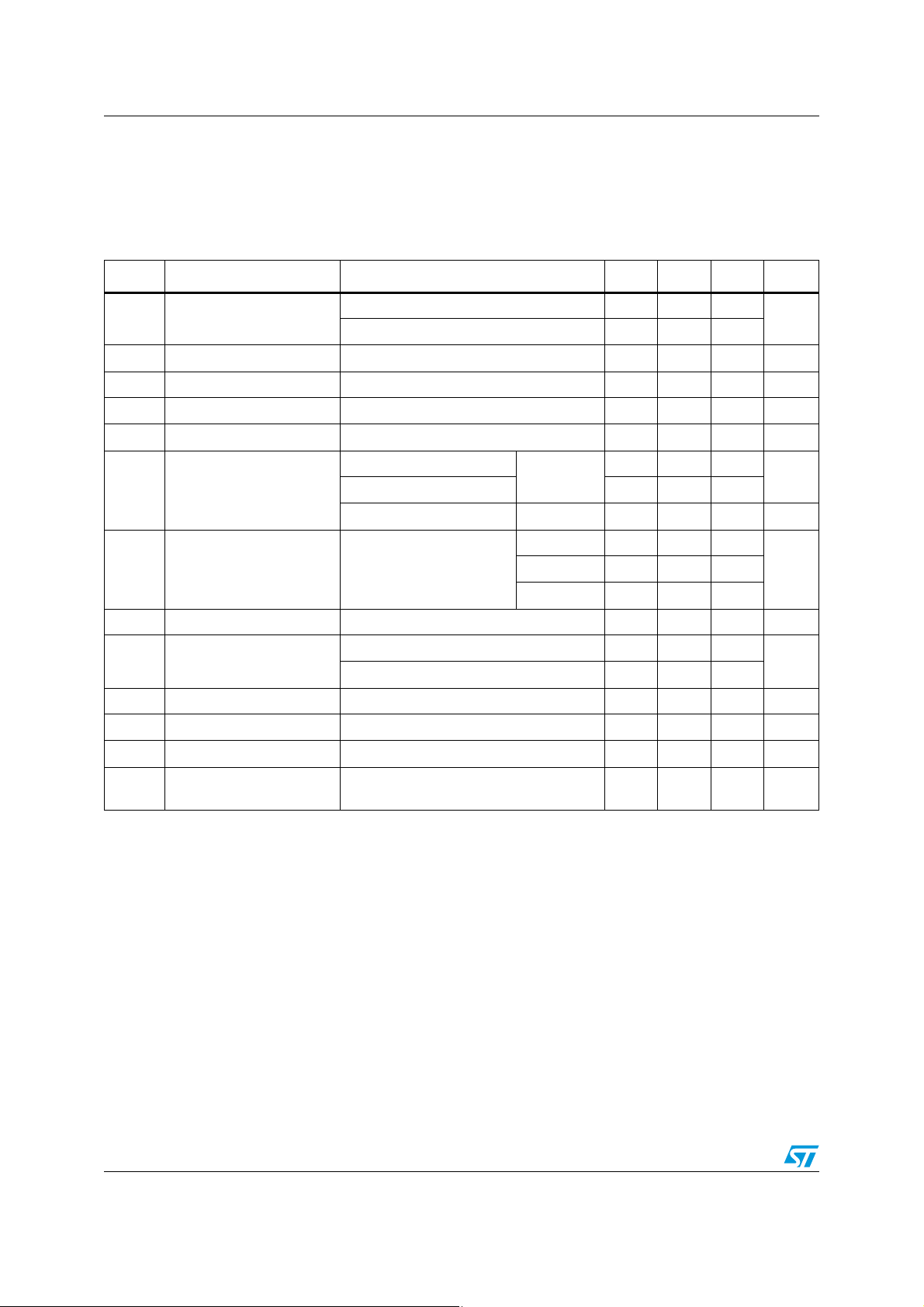
4 Electrical characteristics
Refer to the test circuits, TJ = 25 °C, CI = 0.1 µF, CO = 2.2 µF unless otherwise specified.
Table 4. Electrical characteristics for LE30AB
Symbol Parameter Test conditions Min. Typ. Max. Unit
V
O
V
I
I
O
ΔV
O
ΔV
O
I
d
I
= 10 mA, VI = 5 V 2.970 3 3.030
Output voltage
O
= 10 mA, VI = 5 V, TJ = -25 to 85°C 2.940 3.060
I
O
V
Operating input voltage IO = 100 mA 18 V
Output current limit 150 mA
Line regulation VI = 3.7 to 18 V, IO = 0.5 mA 3 15 mV
Load regulation VI = 4 V, IO = 0.5 to 100 mA 3 15 mV
Quiescent current
= 4 to 18 V, IO = 0 mA
V
I
= 4 to 18 V, IO = 100 mA 1.5 3
V
I
V
= 6 V OFF mode 50 100 µA
I
ON mode
0.5 1
mA
f = 120 Hz 81
SVR Supply voltage rejection I
= 5 mA, VI = 5 ± 1 V
O
f = 10 kHz 60
eN Output noise voltage B = 10 Hz to 100 kHz 50 µV
I
= 100 mA 0.2 0.4
V
Dropout voltage
d
V
Control input logic low TJ = -40 to 125°C 0.8 V
IL
V
Control input logic high TJ = -40 to 125°C 2 V
IH
I
Control input current VI = 6 V, VC = 6 V 10 µA
I
Output bypass
C
O
capacitance
O
= 100 mA, TJ = -40 to 125°C 0.5
I
O
ESR = 0.1 to 10 Ω, I
= 0 to 100 mA 2 10 µF
O
dBf = 1 kHz 76
V
6/22 Doc ID 2573 Rev 13
LExxAB, LExxC Electrical characteristics
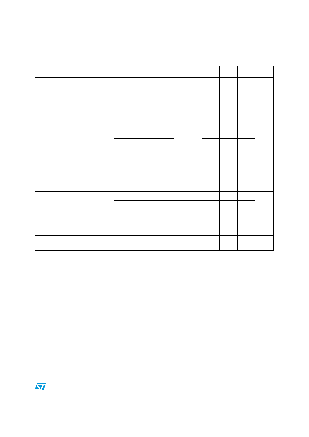
Refer to the test circuits, TJ = 25 °C, CI = 0.1 µF, CO = 2.2 µF unless otherwise specified.
Table 5. Electrical characteristics for LE30C
Symbol Parameter Test conditions Min. Typ. Max. Unit
V
O
V
I
I
O
ΔV
O
ΔVOLoad regulation VI = 4 V, IO = 0.5 to 100 mA 3 25 mV
I
= 10 mA, VI = 5 V 2.940 3 3.060
Output voltage
O
= 10 mA, VI = 5 V, TJ = -25 to 85°C 2.880 3.120
I
O
V
Operating input voltage IO = 100 mA 18 V
Output current limit 150 mA
Line regulation VI = 3.7 to 18 V, IO = 0.5 mA 3 20 mV
Quiescent current
I
d
= 4 to 18 V, IO = 0 mA
V
I
= 4 to 18 V, IO = 100 mA 1.5 3
V
I
ON mode
0.5 1
VI = 6 V OFF mode 50 100 µA
f = 120 Hz 81
SVR Supply voltage rejection I
= 5 mA, VI = 5 ± 1 V
O
f = 10 kHz 60
eN Output noise voltage B = 10 Hz to 100 kHz 50 µV
I
= 100 mA 0.2 0.4
V
Dropout voltage
d
V
Control input logic low TJ = -40 to 125°C 0.8 V
IL
V
Control input logic high TJ = -40 to 125°C 2 V
IH
I
Control input current VI = 6 V, VC = 6 V 10 µA
I
Output bypass
C
O
capacitance
O
IO = 100 mA, TJ = -40 to 125°C 0.5
ESR = 0.1 to 10 Ω, I
= 0 to 100 mA 2 10 µF
O
mA
dBf = 1kHz 76
V
Doc ID 2573 Rev 13 7/22

Electrical characteristics LExxAB, LExxC
Refer to the test circuits, TJ = 25 °C, CI = 0.1 µF, CO = 2.2 µF unless otherwise specified.
Table 6. Electrical characteristics for LE33C
Symbol Parameter Test conditions Min. Typ. Max. Unit
V
O
V
I
I
O
ΔV
O
ΔVOLoad regulation VI = 4.3 V, IO = 0.5 to 100 mA 3 25 mV
I
= 10 mA, VI = 5.3 V 3.234 3.3 3.366
Output voltage
O
= 10 mA, VI = 5.3 V, TJ = -25 to 85°C 3.168 3.432
I
O
V
Operating input voltage IO = 100 mA 18 V
Output current limit 150 mA
Line regulation VI = 4 to 18 V, IO = 0.5 mA 3 20 mV
Quiescent current
I
d
= 4.3 to 18 V, IO = 0 mA
V
I
= 4.3 to 18 V, IO = 100 mA 1.5 3
V
I
ON mode
0.5 1
VI = 6 V OFF mode 50 100 µA
f = 120 Hz 80
SVR Supply voltage rejection I
= 5 mA, VI = 5.3 ± 1 V
O
f = 10 kHz 60
eN Output noise voltage B = 10 Hz to 100 kHz 50 µV
I
= 100 mA 0.2 0.4
V
Dropout voltage
d
V
Control input logic low TJ = -40 to 125°C 0.8 V
IL
V
Control input logic high TJ = -40 to 125°C 2 V
IH
I
Control input current VI = 6 V, VC = 6 V 10 µA
I
Output bypass
C
O
capacitance
O
IO = 100 mA, TJ = -40 to 125°C 0.5
ESR = 0.1 to 10 Ω, I
= 0 to 100 mA 2 10 µF
O
mA
dBf = 1 kHz 75
V
8/22 Doc ID 2573 Rev 13

LExxAB, LExxC Electrical characteristics
Refer to the test circuits, TJ = 25 °C, CI = 0.1 µF, CO = 2.2 µF unless otherwise specified.
Table 7. Electrical characteristics for LE45C
Symbol Parameter Test conditions Min. Typ. Max. Unit
V
O
V
I
I
O
ΔV
O
ΔVOLoad regulation VI = 5.5 V, IO = 0.5 to 100 mA 3 25 mV
I
= 10 mA, VI = 6.5 V 4.41 4.5 4.59
Output voltage
O
= 10 mA, VI = 6.5 V, TJ = -25 to 85°C 4.32 4.68
I
O
V
Operating input voltage IO = 100 mA 18 V
Output current limit 150 mA
Line regulation VI = 5.2 to 18 V, IO = 0.5 mA 4 30 mV
Quiescent current
I
d
= 5.5 to 18 V, IO = 0 mA
V
I
= 5.5 to 18 V, IO = 100 mA 1.5 3
V
I
ON mode
0.5 1
VI = 6 V OFF mode 50 100 µA
f = 120 Hz 77
SVR Supply voltage rejection I
= 5 mA, VI = 6.5 ± 1 V
O
f = 10 kHz 60
eN Output noise voltage B = 10 Hz to 100 kHz 50 µV
I
= 100 mA 0.2 0.4
V
Dropout voltage
d
V
Control input logic low TJ = -40 to 125°C 0.8 V
IL
V
Control input logic high TJ = -40 to 125°C 2 V
IH
I
Control input current VI = 6 V, VC = 6 V 10 µA
I
Output bypass
C
O
capacitance
O
IO = 100 mA, TJ = -40 to 125°C 0.5
ESR = 0.1 to 10 Ω, I
= 0 to 100 mA 2 10 µF
O
mA
dBf = 1 kHz 72
V
Doc ID 2573 Rev 13 9/22

Electrical characteristics LExxAB, LExxC
Refer to the test circuits, TJ = 25 °C, CI = 0.1 µF, CO = 2.2 µF unless otherwise specified.
Table 8. Electrical characteristics for LE50AB
Symbol Parameter Test conditions Min. Typ. Max. Unit
V
O
V
I
I
O
ΔV
O
ΔVOLoad regulation VI = 6 V, IO = 0.5 to 100 mA 3 15 mV
I
= 10 mA, VI = 7 V 4.95 5 5.05
Output voltage
O
= 10 mA, VI = 7 V, TJ = -25 to 85°C 4.9 5.1
I
O
V
Operating input voltage IO = 100 mA 18 V
Output current limit 150 350 425 mA
Line regulation VI = 5.7 to 18 V, IO = 0.5 mA 4 20 mV
Quiescent current
I
d
= 6 to 18 V, IO = 0 mA
V
I
= 6 to 18 V, IO = 100 mA 1.5 3
V
I
ON mode
0.5 1
VI = 6 V OFF mode 50 100 µA
f = 120 Hz 76
SVR Supply voltage rejection I
= 5 mA, VI = 7 ± 1 V
O
f = 10 kHz 60
eN Output noise voltage B = 10 Hz to 100 kHz 50 µV
I
= 100 mA 0.2 0.4
V
Dropout voltage
d
V
Control input logic low TJ = -40 to 125°C 0.8 V
IL
V
Control input logic high TJ = -40 to 125°C 2 V
IH
I
Control input current VI = 6 V, VC = 6 V 10 µA
I
Output bypass
C
O
capacitance
O
IO = 100 mA, TJ = -40 to 125°C 0.5
ESR = 0.1 to 10 Ω, I
= 0 to 100 mA 2 10 µF
O
mA
dBf = 1 kHz 71
V
10/22 Doc ID 2573 Rev 13

LExxAB, LExxC Electrical characteristics
Refer to the test circuits, TJ = 25 °C, CI = 0.1 µF, CO = 2.2 µF unless otherwise specified.
Table 9. Electrical characteristics for LE50C
Symbol Parameter Test conditions Min. Typ. Max. Unit
V
O
V
I
I
O
ΔV
O
ΔVOLoad regulation VI = 6 V, IO = 0.5 to 100 mA 3 25 mV
I
= 10 mA, VI = 7 V 4.9 5 5.1
Output voltage
O
= 10 mA, VI = 7 V, TJ = -25 to 85°C 4.8 5.2
I
O
V
Operating input voltage IO = 100 mA 18 V
Output current limit 150 350 425 mA
Line regulation VI = 5.7 to 18 V, IO = 0.5 mA 4 30 mV
Quiescent current
I
d
= 6 to 18 V, IO = 0 mA
V
I
= 6 to 18 V, IO = 100 mA 1.5 3
V
I
ON mode
0.5 1
VI = 6 V OFF mode 50 100 µA
f = 120 Hz 76
SVR Supply voltage rejection I
= 5 mA, VI = 7 ± 1 V
O
f = 10 kHz 60
eN Output noise voltage B = 10 Hz to 100 kHz 50 µV
I
= 100 mA 0.2 0.4
V
Dropout voltage
d
V
Control input logic low TJ = -40 to 125°C 0.8 V
IL
V
Control input logic high TJ = -40 to 125°C 2 V
IH
I
Control input current VI = 6 V, VC = 6 V 10 µA
I
Output bypass
C
O
capacitance
O
IO = 100 mA, TJ = -40 to 125°C 0.5
ESR = 0.1 to 10 Ω, I
= 0 to 100 mA 2 10 µF
O
mA
dBf = 1 kHz 71
V
Doc ID 2573 Rev 13 11/22

Electrical characteristics LExxAB, LExxC
Refer to the test circuits, TJ = 25 °C, CI = 0.1 µF, CO = 2.2 µF unless otherwise specified.
Table 10. Electrical characteristics for LE80C
Symbol Parameter Test conditions Min. Typ. Max. Unit
V
O
V
I
I
O
ΔV
O
ΔVOLoad regulation VI = 9 V, IO = 0.5 to 100 mA 3 25 mV
I
= 10 mA, VI = 10 V 7.84 8 8.16
Output voltage
O
= 10 mA, VI = 10 V, TJ = -25 to 85°C 7.68 8.32
I
O
V
Operating input voltage IO = 100 mA 18 V
Output current limit 150 mA
Line regulation VI = 8.7 to 18 V, IO = 0.5 mA 5 35 mV
Quiescent current
I
d
= 9 to 18 V, IO = 0 mA
V
I
= 9 to 18 V, IO = 100 mA 1.7 3.6
V
I
ON mode
0.7 1.6
VI = 9 V OFF mode 70 140 µA
f = 120 Hz 72
SVR Supply voltage rejection I
= 5 mA, VI = 10 ± 1 V
O
f = 10 kHz 57
eN Output noise voltage B = 10 Hz to 100 kHz 50 µV
I
= 100 mA 0.2 0.4
V
Dropout voltage
d
V
Control input logic low TJ = -40 to 125°C 0.8 V
IL
V
Control input logic high TJ = -40 to 125°C 2 V
IH
I
Control input current VI = 9 V, VC = 6 V 10 µA
I
Output bypass
C
O
capacitance
O
IO = 100 mA, TJ = -40 to 125°C 0.5
ESR = 0.1 to 10 Ω, I
= 0 to 100 mA 2 10 µF
O
mA
dBf = 1 kHz 66
V
12/22 Doc ID 2573 Rev 13

LExxAB, LExxC Typical performance characteristics
5 Typical performance characteristics
Unless otherwise specified, V
Figure 4. Dropout voltage vs. output current Figure 5. Dropout voltage vs. temperature
Figure 6. Supply current vs. temperature Figure 7. Supply current vs. input voltage
O(NOM)
= 3.3 V.
Figure 8. Short-circuit current vs. dropout
voltage
Doc ID 2573 Rev 13 13/22
Figure 9. SVR vs. frequency

Typical performance characteristics LExxAB, LExxC
Figure 10. Logic-controlled precision 3.3/5.0 V selectable output
Figure 11. Sequential multi-output supply
14/22 Doc ID 2573 Rev 13

LExxAB, LExxC Typical performance characteristics
Figure 12. Multiple supplies with ON/OFF toggle switch
Figure 13. Basic inhibit functions
Doc ID 2573 Rev 13 15/22

Package mechanical data LExxAB, LExxC
6 Package mechanical data
In order to meet environmental requirements, ST offers these devices in different grades of
ECOPACK
specifications, grade definitions and product status are available at:
ECOPACK
®
packages, depending on their level of environmental compliance. ECOPACK®
®
is an ST trademark.
www.st.com
.
16/22 Doc ID 2573 Rev 13

LExxAB, LExxC Package mechanical data
SO-8 mechanical data
Dim.
A1.35 1.75 0.053 0.069
A1 0.10 0.25 0.04 0.010
A2 1.10 1.65 0.043 0.065
B0.33 0.51 0.013 0.020
C0.19 0.25 0.007 0.010
D4.80 5.00 0.189 0.197
E 3.80 4.00 0.150 0.157
e 1.27 0.050
H5.80 6.20 0.228 0.244
h 0.25 0.50 0.010 0.020
L 0.40 1.27 0.016 0.050
k 8° (max.)
ddd 0.1 0.04
Min. Typ. Max. Min. Typ. Max.
mm. inch.
0016023/C
Doc ID 2573 Rev 13 17/22

Package mechanical data LExxAB, LExxC
TO-92 mechanical data
mm. mils.
Dim.
Min. Typ. Max. Min. Typ. Max.
A4.324.95 170.1 194.9
b 0.36 0.51 14.2 20.1
D 4.45 4.95 175.2 194.9
E 3.30 3.94129.9 155.1
e 2.41 2.67 94.9 105.1
e1 1.14 1.40 44.9 55.1
L 12.7 15.49 500.0 609.8
R 2.16 2.41 85.0 94.9
S10.92 1.52 36.2 59.8
W 0.41 0.56 16.1 22.0
α 5° 5°
18/22 Doc ID 2573 Rev 13
0102782/D

LExxAB, LExxC Package mechanical data
Tape & reel SO-8 mechanical data
mm. inch.
Dim.
Min. Typ. Max. Min. Typ. Max.
A 330 12.992
C 12.8 13.2 0.504 0.519
D 20.2 0.795
N60 2.362
T 22.4 0.882
Ao 8.1 8.5 0.319 0.335
Bo 5.5 5.9 0.216 0.232
Ko 2.1 2.3 0.082 0.090
Po 3.9 4.1 0.153 0.161
P7.98.1 0.311 0.319
Doc ID 2573 Rev 13 19/22

Package mechanical data LExxAB, LExxC
Tape & reel for TO-92 mechanical data
Dim.
Min. Typ. Max. Min. Typ. Max.
mm. inch.
A1 4.80 0.189
T 3.80 0.150
T1 1.60 0.063
T2 2.30 0.091
d0.48 0.019
P0 12.5 12.9 0.492 0.508
P2 5.65 7.05 0.222 0.278
F1, F2 2.44 2.54 2.94 0.096 0.100 0.116
delta H ±2 0.079
W 17.5 18.00 19.0 0.689 0.709 0.748
W0 5.7 6.3 0.224 0.248
W1 8.5 9.25 0.3350.364
W2 0.50 0.20
H18.50 18.70 0.728 0.726
H0 15.50 16.50 0.610 0.650
H1 25.00 0.984
D0 3.8 4.2 0.150 0.165
t0.900.035
L1 3 0.118
delta P±1 0.039
u 50 1.968
Φ1 3
60 14.173
Φ2 301.181
H1
delta P
A1
delta H
H
H0
L
d
W2
T
T2
T1
l1
20/22 Doc ID 2573 Rev 13
P2
F1
F2
P0
DRAWING NOT IN SCALE
D0
W0
W
W1
t

LExxAB, LExxC Revision history
7 Revision history
Table 11. Document revision history
Date Revision Changes
09-Jul-2004 6 I
16-Mar-2005 7 Add Tape & Reel for TO-92 - Note on Table 3.
12-Feb-2007 8 Change value T
26-Jul-2007 9 Add Table 1 in cover page.
29-Nov-2007 10 Modified: Table 25.
12-Feb-2008 11 Modified: Table 25.
10-Jul-2008 12 Modified: Table 1 and Table 25.
22-May-2012 13
typ. and max. are changed in tab. 24 and 25 - pag. 14.
O
on Table 2.
OP
Updated:
Changed: TA in TJ test conditions from table 4 to table 10.
Table 1 on page 1
.
Doc ID 2573 Rev 13 21/22

LExxAB, LExxC
Please Read Carefully:
Information in this document is provided solely in connection with ST products. STMicroelectronics NV and its subsidiaries (“ST”) reserve the
right to make changes, corrections, modifications or improvements, to this document, and the products and services described herein at any
time, without notice.
All ST products are sold pursuant to ST’s terms and conditions of sale.
Purchasers are solely responsible for the choice, selection and use of the ST products and services described herein, and ST assumes no
liability whatsoever relating to the choice, selection or use of the ST products and services described herein.
No license, express or implied, by estoppel or otherwise, to any intellectual property rights is granted under this document. If any part of this
document refers to any third party products or services it shall not be deemed a license grant by ST for the use of such third party products
or services, or any intellectual property contained therein or considered as a warranty covering the use in any manner whatsoever of such
third party products or services or any intellectual property contained therein.
UNLESS OTHERWISE SET FORTH IN ST’S TERMS AND CONDITIONS OF SALE ST DISCLAIMS ANY EXPRESS OR IMPLIED
WARRANTY WITH RESPECT TO THE USE AND/OR SALE OF ST PRODUCTS INCLUDING WITHOUT LIMITATION IMPLIED
WARRANTIES OF MERCHANTABILITY, FITNESS FOR A PARTICULAR PURPOSE (AND THEIR EQUIVALENTS UNDER THE LAWS
OF ANY JURISDICTION), OR INFRINGEMENT OF ANY PATENT, COPYRIGHT OR OTHER INTELLECTUAL PROPERTY RIGHT.
UNLESS EXPRESSLY APPROVED IN WRITING BY TWO AUTHORIZED ST REPRESENTATIVES, ST PRODUCTS ARE NOT
RECOMMENDED, AUTHORIZED OR WARRANTED FOR USE IN MILITARY, AIR CRAFT, SPACE, LIFE SAVING, OR LIFE SUSTAINING
APPLICATIONS, NOR IN PRODUCTS OR SYSTEMS WHERE FAILURE OR MALFUNCTION MAY RESULT IN PERSONAL INJURY,
DEATH, OR SEVERE PROPERTY OR ENVIRONMENTAL DAMAGE. ST PRODUCTS WHICH ARE NOT SPECIFIED AS "AUTOMOTIVE
GRADE" MAY ONLY BE USED IN AUTOMOTIVE APPLICATIONS AT USER’S OWN RISK.
Resale of ST products with provisions different from the statements and/or technical features set forth in this document shall immediately void
any warranty granted by ST for the ST product or service described herein and shall not create or extend in any manner whatsoever, any
liability of ST.
ST and the ST logo are trademarks or registered trademarks of ST in various countries.
Information in this document supersedes and replaces all information previously supplied.
The ST logo is a registered trademark of STMicroelectronics. All other names are the property of their respective owners.
© 2012 STMicroelectronics - All rights reserved
STMicroelectronics group of companies
Australia - Belgium - Brazil - Canada - China - Czech Republic - Finland - France - Germany - Hong Kong - India - Israel - Italy - Japan -
Malaysia - Malta - Morocco - Philippines - Singapore - Spain - Sweden - Switzerland - United Kingdom - United States of America
www.st.com
22/22 Doc ID 2573 Rev 13
 Loading...