

Datasheet LE28C1001M-90, LE28C1001M-12, LE28C1001T-90, LE28C1001T-15, LE28C1001T-12 Datasheet (SANYO)
Page 1
CMOS LSI
Ordering number : EN*5129A
D3096HA (OT)/N3095HA (OT) No. 5129-1/14
Preliminary
SANYO Electric Co.,Ltd. Semiconductor Bussiness Headquarters
TOKYO OFFICE Tokyo Bldg., 1-10, 1 Chome, Ueno, Taito-ku, TOKYO, 110 JAPAN
1MEG (131072 words × 8 bits) Flash Memory
LE28C1001M, T-90/12/15
Overview
The LE28C1001M, T series ICs are 1 MEG flash memory
products that feature a 131072-word × 8-bit organization
and 5 V single-voltage power supply operation. CMOS
peripheral circuits are adopted for high speed, low power
dissipation, and ease of use. A 128-byte page rewrite
function provides rapid data rewriting.
Features
• Highly reliable 2-layer polysilicon CMOS flash
EEPROM process
• Read and write operations using a 5 V single-voltage
power supply
• Fast access time: 90, 120, and 150 ns
• Low power dissipation
— Operating current (read): 30 mA (maximum)
— Standby current: 20 µA (maximum)
• Highly reliable read/write
— Erase/write cycles: 104/103cycles
— Data retention: 10 years
• Address and data latches
• Fast page rewrite operation
— 128 bytes per page
— Byte/page rewrite time: 5 ms (typical)
— Chip rewrite time: 5 s (typical)
• Automatic rewriting using internally generated Vpp
• Rewrite complete detection function
— Toggle bit
— Data polling
• Hardware and software data protection functions
• All inputs and outputs are TTL compatible.
• Pin assignment conforms to the JEDEC byte-wide
EEPROM standard.
• Package
SOP 32-pin (525 mil) plastic package : LE28C1001M
TSOP 32-pin (8 ×20 mm)plastic package : LE28C1001T
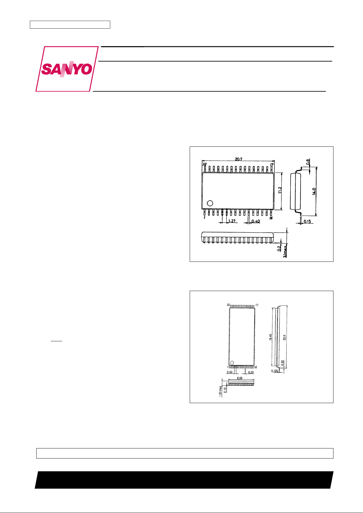
Package Dimensions
unit: mm
3205-SOP32
unit: mm
3224-TSOP32
SANYO: TSOP32 (TYPE-I)
[LE28C1001T]
These FLASH MEMORY products incorporate technology licensed Silicon Storage Technology, Inc.
[LE28C1001M]
SANYO: SOP32
Page 2
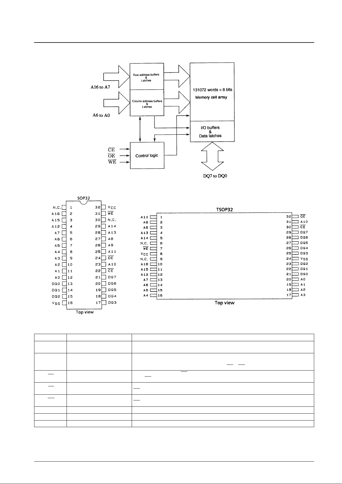
Block Diagram
Pin Assignments
Pin Functions
No. 5129-2/14
LE28C1001M, T-90/12/15
Symbol Pin Function
A16 to A0 Address input
Supply the memory address to these pins.
The address is latched internally during a write cycle.
These pins output data during a read cycle and input data during a write cycle.
DQ7 to DQ0 Data input and output Data is latched internally during a write cycle.
Outputs go to the high-impedance state when either OE or CE is high.
CE Chip enable
The device is active when CE is low.
When CE is high, the device becomes unselected and goes to the standby state.
OE Output enable
Makes the data output buffers active.
OE is an active-low input.
WE Write enable
Makes the write operation active.
WE is an active-low input.
V
CC
Power supply Apply 5 V (±10%) to this pin.
V
SS
Ground
N.C. No connection These pins must be left open.
A05759
A05760
Page 3
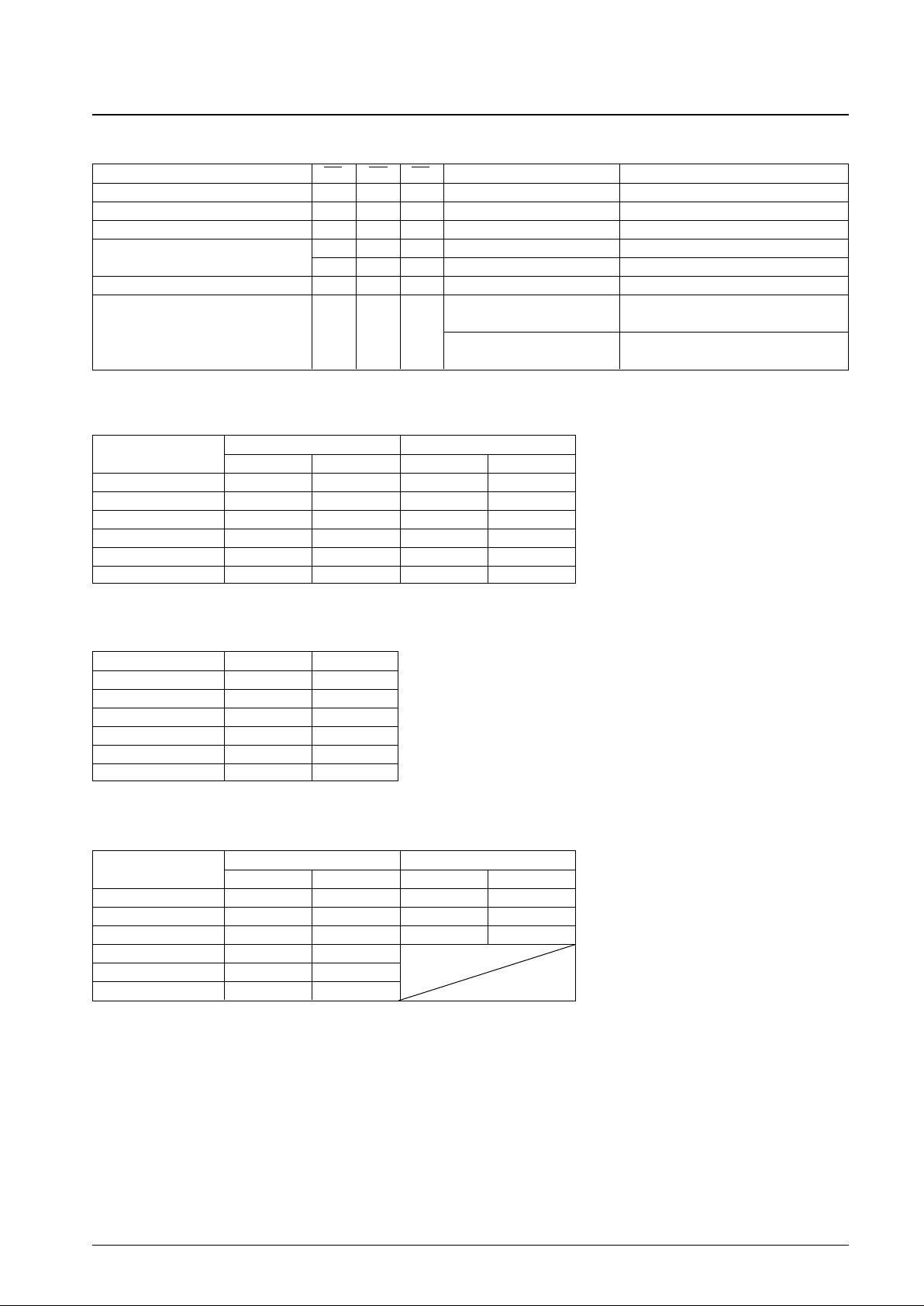
Function Logic
Software Data Protection Command
Note: Address format A14 to A0 (hex.)
Software Chip Erase Command (5 V single-voltage power supply)
Note: Address format A14 to A0 (hex.)
Software Product ID Entry Command and Exit Command Codes
Notes on software Product ID Command Code:
1. Command Code Address format: A14 to A0 (hex.)
2. With A14 to A1 = V
IL
,
Manufacturer Code is read with A0 = V
IL
to be BFH
LE28C1001M, T series Device Code is read with A0 = V
IH
to be 07H
3. The device does not remain in Software Product ID Mode if powered down.
4. A16 and A15 are V
IH
or V
IL.
No. 5129-3/14
LE28C1001M, T-90/12/15
Mode CE OE WE A16 to A0 DQ7 to DQ0
Read V
IL
V
IL
VIHA
IN
D
OUT
Write V
IL
V
IH
VILA
IN
D
IN
Standby V
IH
X X X High-Z
Write inhibit
X V
IL
X X High-Z/D
OUT
X X VIHX High-Z/D
OUT
Software chip erase (5 V, single voltage) V
IL
V
IH
VILA
IN
D
IN
A16 to A10 = VIL, A8 to A1 = VIL,
Manufacturer code (BF)
A9 = 12 V, A0 = V
IL
Product identification V
IL
V
IL
V
IH
A16 to A10 = VIL, A8 to A1 = VIL,
Device code (07)
A9 = 12 V, A0 = V
IH
Byte sequence
Set protection Reset protection
Address Data Address Data
Write 0 5555 AA 5555 AA
Write 1 2AAA 55 2AAA 55
Write 2 5555 A0 5555 80
Write 3 5555 AA
Write 4 2AAA 55
Write 5 5555 20
Byte sequence
Protect ID Entry Protect ID Exit
Address Data Address Data
Write 0 5555 AA 5555 AA
Write 1 2AAA 55 2AAA 55
Write 2 5555 80 5555 F0
Write 3 5555 AA
Write 4 2AAA 55
Write 5 5555 60
Byte sequence Address Data
Write 0 5555 AA
Write 1 2AAA 55
Write 2 5555 80
Write 3 5555 AA
Write 4 2AAA 55
Write 5 5555 10
Page 4

Device Operation
This Sanyo 1 MEG flash memory allows electrical rewrites using a 5 V single-voltage power supply. The LE28C1001M,
T series products are pin and function compatible with the industry standards for this type of product.
Read
The LE28C1001M, T series read operations are controlled by CE and OE. The host must set both pins to the low level to
acquire the output data. CE is used for chip selection. When CE is at the high level, the chip will be in the unselected
state and only draw the standby current. OE is used for output control. The output pins go to the high-impedance state
when either CE or OE is high. See the timing waveforms (Figure 1) for details.
Page Write Operation
The write operation starts when both CE and WE are at the low level, and furthermore OE is at the high level. The write
operation is executed in two stages. The first stage is a byte load cycle in which the host writes to the LE28C1001M, T
series internal page buffers. The second stage is an internal programming cycle in which the data in the page buffer is
written to the nonvolatile memory cell array. In the byte load cycle, the address is latched on the falling edge of either
CE or WE, whichever occurs later. The input data is latched on the rising edge of either CE or WE, whichever occurs
first. The internal programming cycle starts if either WE or CE remains high for 200 µs (t
BLCO
). Once this programming
cycle starts, the operation continues until the programming operation is completely done. This operation executes within
5 ms (typical). Figures 2 and 3 show the WE and CE control write cycle timing diagrams, and Figure 10 shows the
flowchart for this operation.
In the page write operation, 128 bytes of data can be written to the LE28C1001M, T series internal page buffer before
the internal programming cycle. All the data in the page buffer is written to the memory cell array during the 5 ms
(typical) internal programming cycle. Therefore the LE28C1001M, T series page write function can rewrite all memory
cells in 5 seconds (typical). The host can perform any other activities desired, such as moving data at other locations
within the system and preparing the data required for the next page write, during the period prior to the completion of the
internal programming cycle. In a given page write operation, all the data bytes loaded into the page buffers must be for
the same page address specified by address lines A7 through A16. All data that was not explicitly loaded into the page
buffer is set to FFH.
Figure 2 shows the page write cycle timing diagram. If the host loads the second data byte into the page buffer within the
100 µs byte load cycle time (t
BLC
) after the first byte load cycle the LE28C1001M, T series stop in the page load cycle
thus allowing data to be loaded continuously. The page load cycle terminates if additional data is not loaded into the
internal page buffer within 200 µs (t
BLCO
) after the previous byte load cycle, as in the case where WE does not switch
from high to low after the last WE rising edge. The data in the page buffer can be rewritten in the next byte load cycle.
The page load period can continue indefinitely as long as the host continues to load data into the device within the 100 µs
byte load cycle. The page that is loaded is determined by the page address of the last byte loaded.
Detecting the Write Operation State
The LE28C1001M, T series products provide two functions for detecting the completion of the write cycle. These
functions are used to optimize the system write cycle time. These functions are based on detecting the states of the Data
polling bit (DQ7) and the toggle bit (DQ6).
Data Polling (DQ7)
The LE28C1001M, T series products output to DQ7 the inverse of the last data loaded during the page and byte load
cycles when the internal programming cycle is in progress. The last data loaded can be read from DQ7 when the internal
programming cycle completes. Figure 4 shows the Data polling cycle timing diagram and Figure 11 shows the flowchart
for this operation.
Toggle Bit (DQ6)
Data values of 0 and 1 are output alternately for DQ6, that is DQ6 is toggled between 0 and 1, during the internal
programming cycle. When the internal programming cycle completes this toggling is stopped and the device becomes
ready to execute the next operation. Figure 5 shows the toggle bit timing diagram and Figure 11 shows the flowchart for
this operation.
No. 5129-4/14
LE28C1001M, T-90/12/15
Page 5

Data Protection
Hardware Data Protection
Noise and glitch protection: The LE28C1001M, T series do not execute write operations for WE or OE pulses that are 15
ns or shorter.
Power (VCC) on and cutoff detection: The programming operation is disabled when VCCis 2.5 V or lower.
Write inhibit mode: Writing is disabled when OE is low and either CE is high or WE is high. Use this function to prevent
writes from occurring when the power is being turned on or off.
Software Data Protection
The LE28C1001M, T series implement the optional software data protection function recognized by JEDEC. This
function requires a 3-byte load operation to be performed before a write operation data load. The 3-byte load sequence
starts a page load cycle without activating any write operation. Thus this is an optimal protection scheme for unintended
write cycles triggered by noise associated with powering the chip on or off. Note that the LE28C1001M, T series are
shipped with the software data protection function disabled.
The software data protection circuit is activated by executing a 3-byte byte load cycle in advance of the data sequence in
the page load cycle. (See Figure 6.) This causes the device to automatically enter data protection mode. After this, write
operations require a 3-byte byte load cycle to be executed in advance. A 6-byte write sequence is required to switch the
device out of this protection mode. Figure 7 shows the timing diagram. If a write operation is attempted in software
protection mode, all device functions are disabled for 200 µs. Figure 12 shows the flowchart for this operation.
Chip Erase
The LE28C1001M, T series provide a chip erase mode that erases all of the memory cell array and sets each bit to the 1
state. This mode can be effective when it is necessary to erase all data quickly.
5 V Single-Voltage Power Supply Software Chip Erase
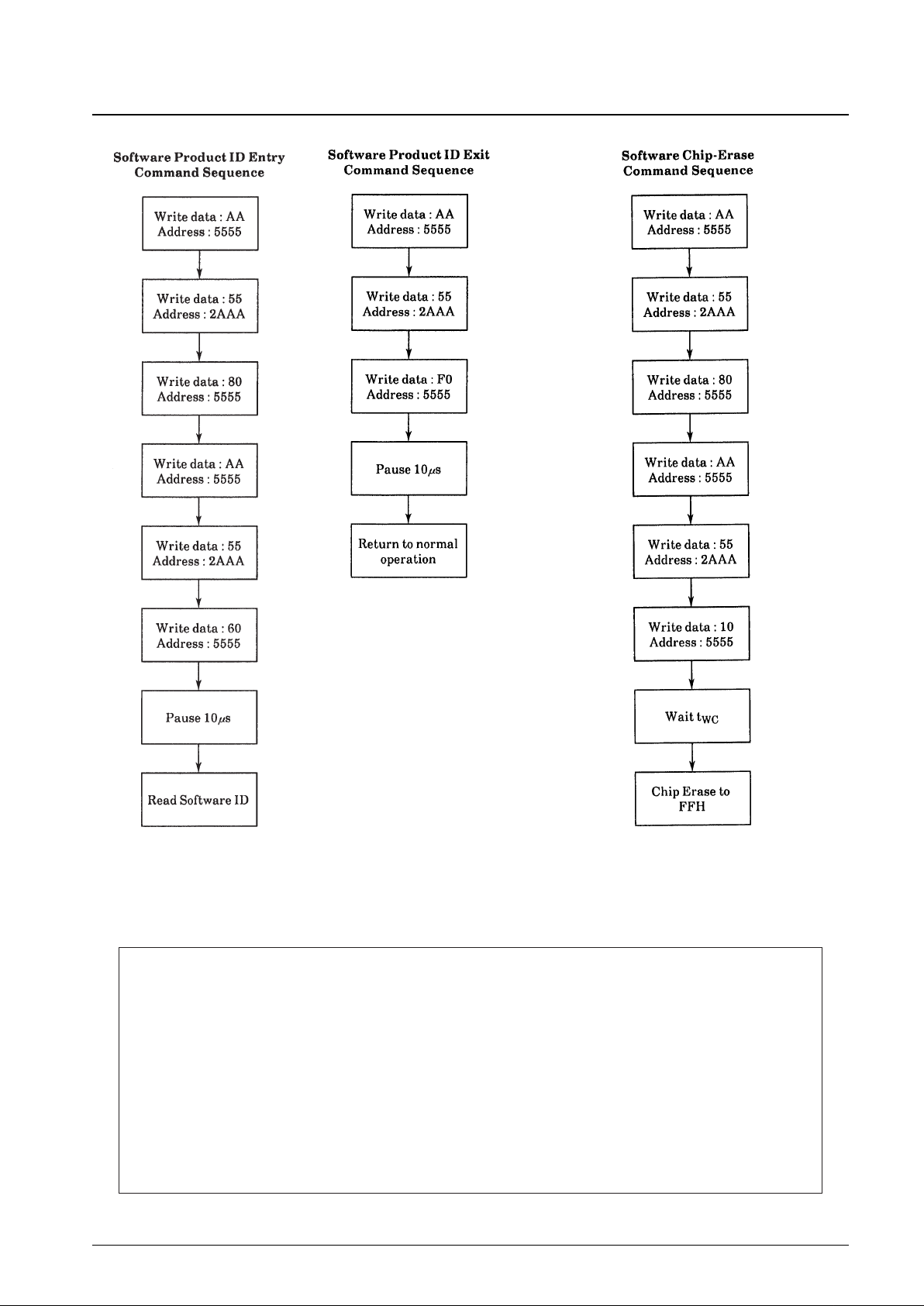
The software chip erase mode operation is started by executing a specially defined 6-byte byte load sequence, similar to
page mode operation under software protection. After the load cycle is executed, the device enters an internal
programming cycle similar to the write cycle. Figure 8 shows the timing diagram and Figure 14 shows the flowchart for
this operation.
Product Identification
The device identification code is used for recognizing the device and its manufacturer. This mode can be used by
hardware and software. The hardware operating mode is used to recognize algorithms that match the device when an
external programming unit is used. Also, user systems can recognize the product number using software product
identification mode. Figure 13 shows the flowchart for this operation. The manufacturer and device codes are the same
in both modes.
No. 5129-5/14
LE28C1001M, T-90/12/15
Page 6
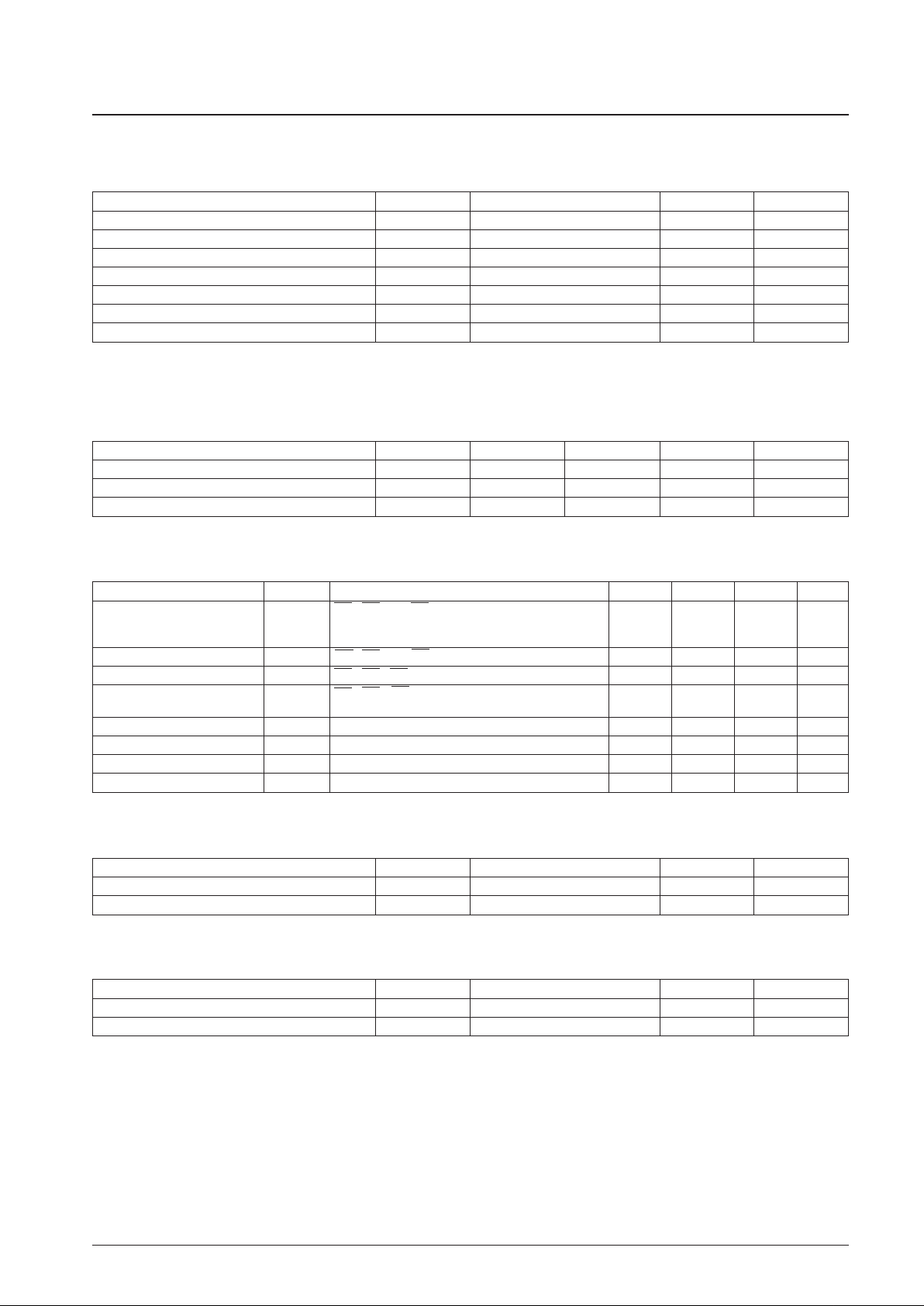
Specifications
Absolute Maximum Ratings at Ta 25°C
Note: 1. The device may be destroyed by the application of stresses in excess of the absolute maximum ratings.
2. –1.0 V to V
CC
+ 1.0 V for pulses less than 20 ns
3. –1.0 V to +14 V for pulses less than 20 ns
DC Recommended Operating Ranges at Ta = 0 to +70°C
DC Electrical Characteristics at Ta = 0 to +70°C, VCC= 5 V ± 10%
Input/output Capacitances at Ta = 25°C, VCC= 5 V ± 10%, f = 1 MHz
Power on Timing
No. 5129-6/14
LE28C1001M, T-90/12/15
Parameter Symbol Ratings Unit Note
Supply voltage V
CC
–0.5 to +6.0 V 1
Input pin voltage V
IN
–0.5 to VCC+ 0.5 V 1, 2
DQ pin voltage V
OUT
–0.5 to VCC+ 0.5 V 1, 2
A9 pin voltage V
A9
–0.5 to +14.0 V 1, 3
Allowable power dissipation Pd max 600 mW 1, 4
Operating temperature Topr 0 to +70 °C 1
Storage temperature Tstg –65 to +150 °C 1
Parameter Symbol min typ max Unit
Supply voltage V
CC
4.5 5.0 5.5 V
Input low-level voltage V
IL
0.8 V
Input high-level voltage V
IH
2.0 V
Parameter Symbol Conditions max Unit
Input/output capacitance C
DQ
VDQ= 0 V 12 pF
Input capacitance C
IN
VIN= 0 V 6 pF
Parameter Symbol Conditions max Unit
Time from power on until first read operation t
PU-READ
100 µs
Time from power on until first write operation t
PU-WRITE
5 ms
Parameter Symbol Conditions min typ max Unit
CE = OE = V
IL
, WE = VIH, all DQ pins open,
Current drain during read I
CCR
address inputs = VIHor VIL, operating frequency = 30 mA
1/t
RC
(minimum), VCC= VCCmax
Current drain during write I
CCW
CE = WE = VIL, OE = VIH, VCC= VCCmax 50 mA
TTL standby current I
SB1
CE = OE = WE =VIH,VCC= VCCmax 3 mA
CMOS standby current I
SB2
CE = OE = WE =VCC– 0.3 V,
20 µA
V
CC
= VCCmax
Input leakage current I
LI
VIN= VSSto VCC, VCC= VCCmax 10 µA
Output leakage current I
LO
VIN= VSSto VCC, VCC= VCCmax 10 µA
Output low-level voltage V
OL
IOL= 2.1 mA, VCC= VCCmin 0.4 V
Output high-level voltage V
OHIOH
= –400 µA, VCC= VCCmin 2.4 V
Page 7
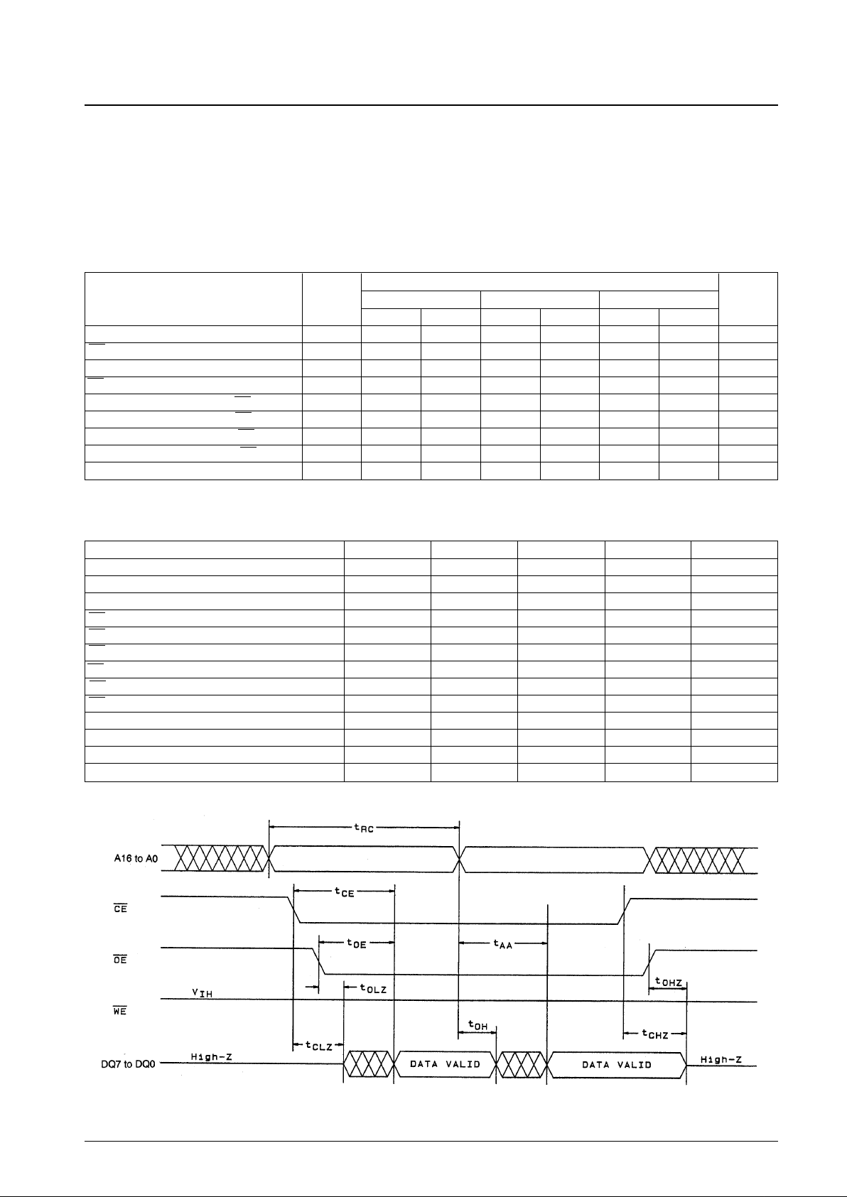
AC Electrical Characteristics at Ta = 0 to +70°C, VCC= 5 V ± 10%
AC Testing Conditions (See Figure 9)
Input rise and fall times: ................10 ns (max.)
Output load:....................................1 TTL gate + 100 pF
Read Cycle
Page Write Cycle
Note: * typ is a reference value at VCC= 5.0, Ta = 25 °C.
Figure 1 Read Cycle
No. 5129-7/14
LE28C1001M, T-90/12/15
Parameter Symbol min typ* max Unit
Write cycle time (erase and program) t
WC
5 10 ms
Address setup time t
AS
0 ns
Address hold time t
AH
50 ns
CE setup time t
CS
0 ns
CE hold time t
CH
0 ns
OE setup time t
OES
0 ns
OE hold time t
OEH
0 ns
CE pulse width t
CP
70 ns
WE pulse width t
WP
70 ns
Data setup time t
DS
45 ns
Data hold time t
DH
0 ns
Byte load cycle time t
BLC
0.05 100 µs
Byte load timeout time t
BLCO
200 µs
LE28C1001M, T
Parameter Symbol -90 -12 -15 Unit
min max min max min max
Read cycle time t
RC
90 120 150 ns
CE access time t
CE
90 120 150 ns
Address access time t
AA
90 120 150 ns
OE access time t
OE
50 60 70 ns
Output low-impedance time from CE t
CLZ
0 0 0 ns
Output low-impedance time from OE t
OLZ
0 0 0 ns
Output high-impedance time from CE t
CHZ
40 40 40 ns
Output high-impedance time from OE t
OHZ
40 40 40 ns
Output valid time from address input t
OH
0 0 0 ns
A05761
Page 8
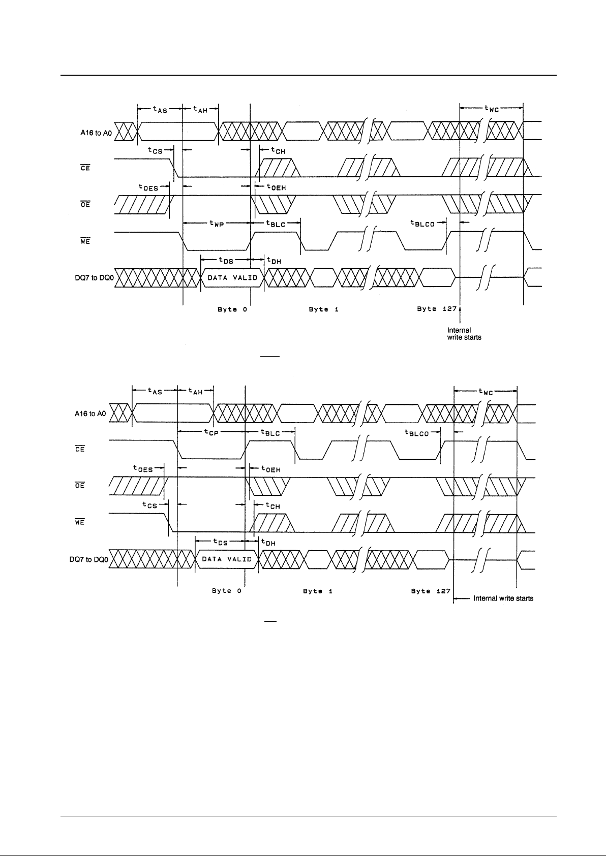
Figure 2 WE Control Page Write Cycle
Figure 3 CE Control Page Write Cycle
No. 5129-8/14
LE28C1001M, T-90/12/15
A05762
A05763
Page 9
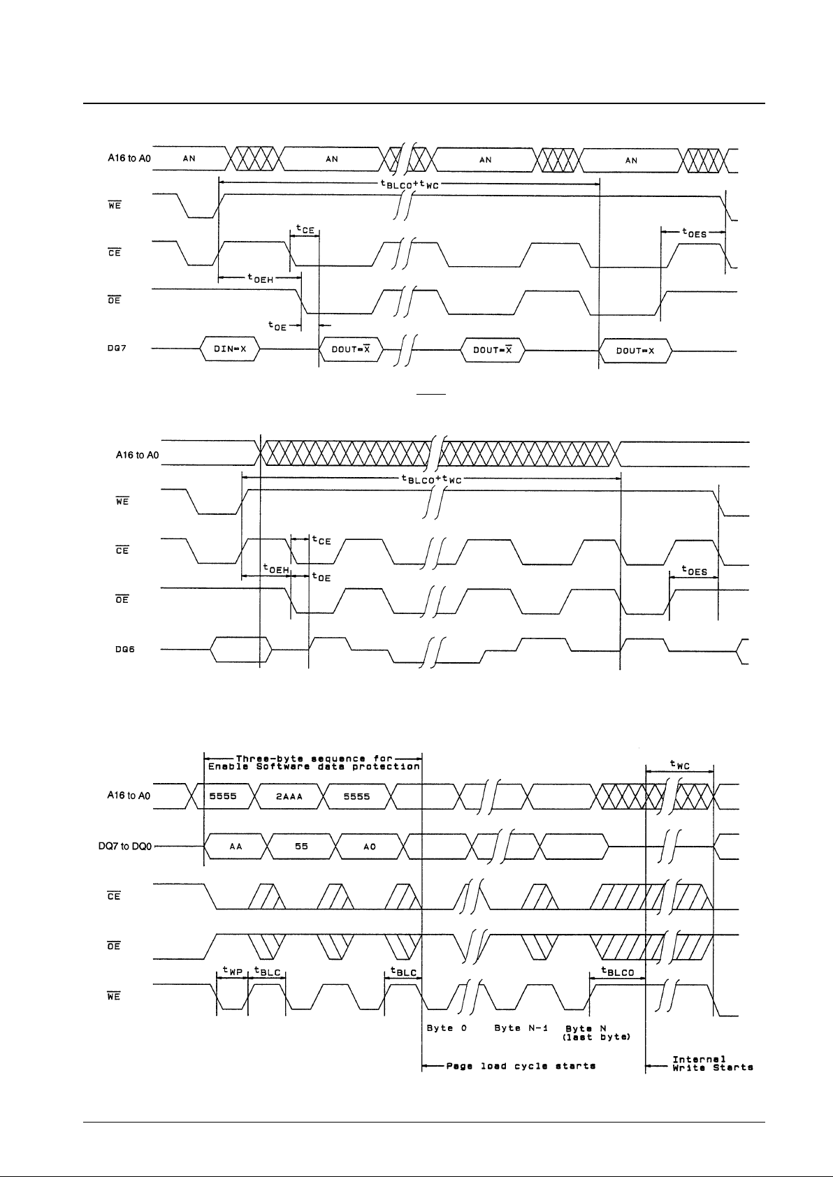
Figure 4 Data Polling
Figure 5 Toggle Bit
Figure 6 Enable Software Data Protection
No. 5129-9/14
LE28C1001M, T-90/12/15
A05764
A05765
A05766
Page 10
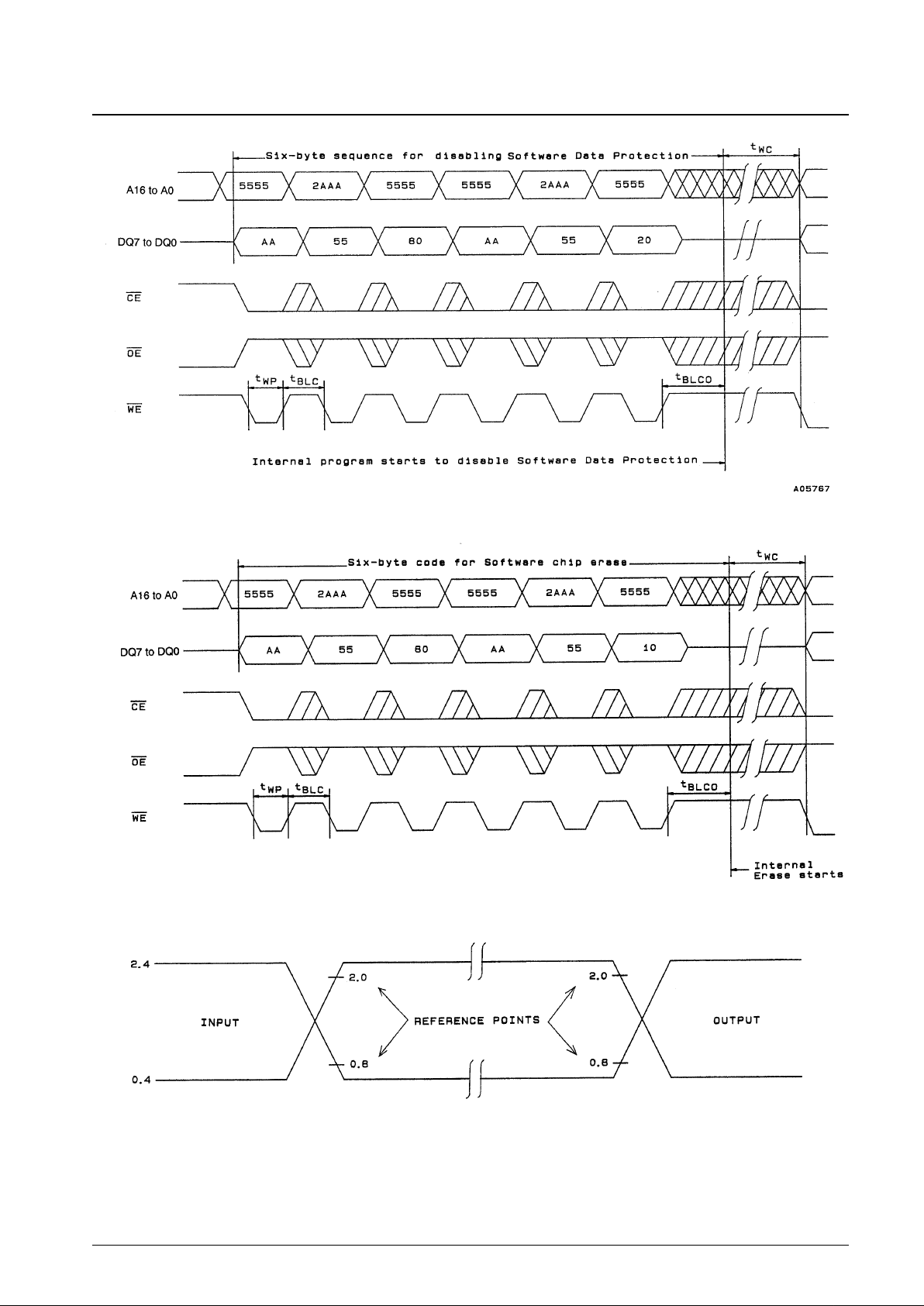
Figure 7 Disable Software Data Protection
Figure 8 Software Chip Erase
AC test inputs are driven at VOH(2.4 V) for a logic 1 and at VOL(0.4 V) for a logic 0. The I/O measurement reference points are VIH(2.0 V) and VIL(0.8 V).
The input rise and fall times (10% ↔ 90%) must be 10 ns or shorter.
Figure 9 AC I/O Reference Waveform
No. 5129-10/14
LE28C1001M, T-90/12/15
A05768
A05769
Page 11
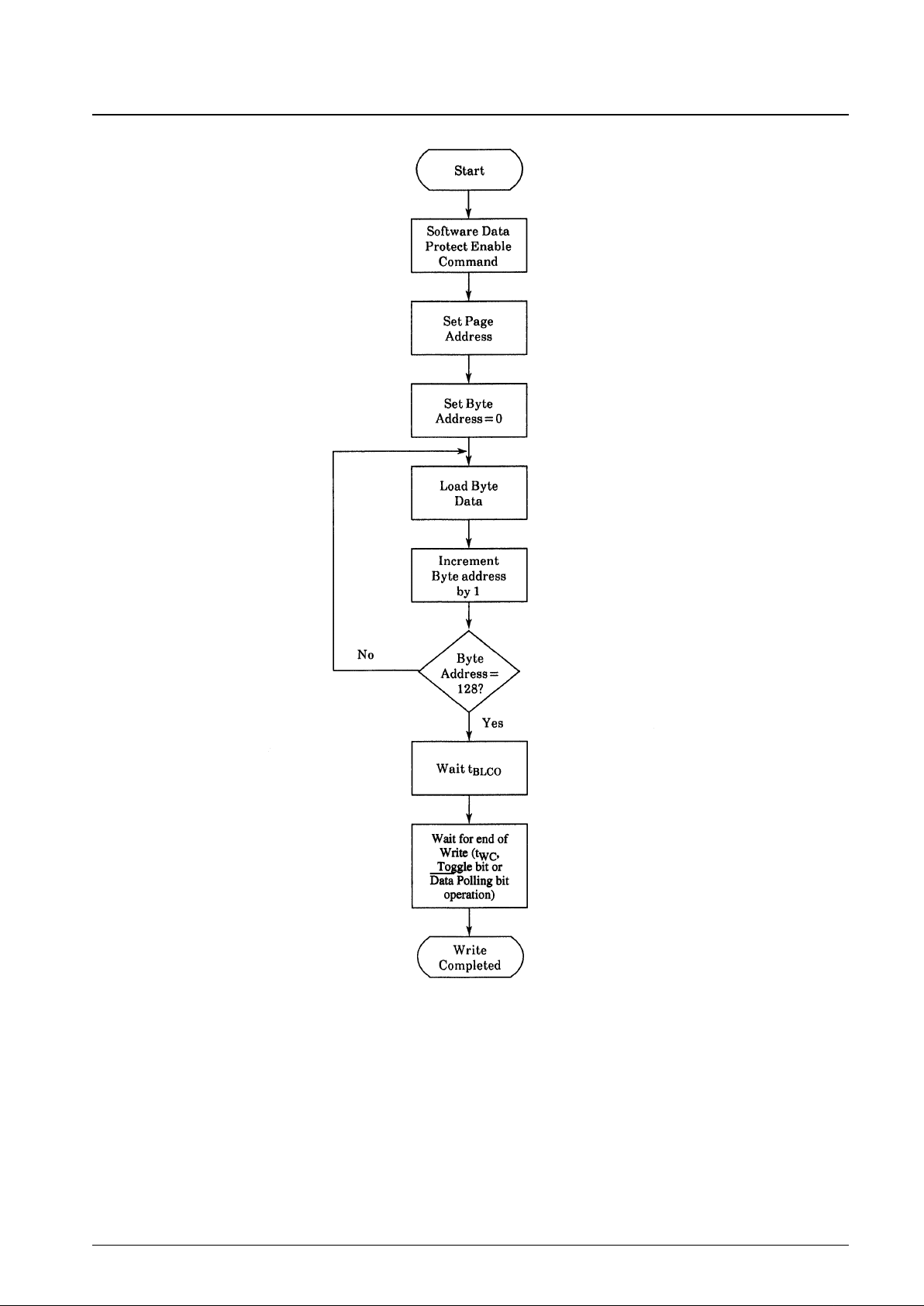
Figure 10 Write Algorithm
No. 5129-11/14
LE28C1001M, T-90/12/15
Page 12
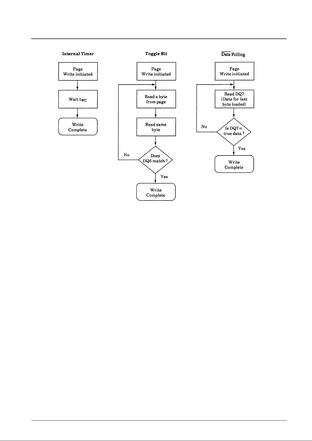
Figure 11 Write Operating State Detection
No. 5129-12/14
LE28C1001M, T-90/12/15
Page 13
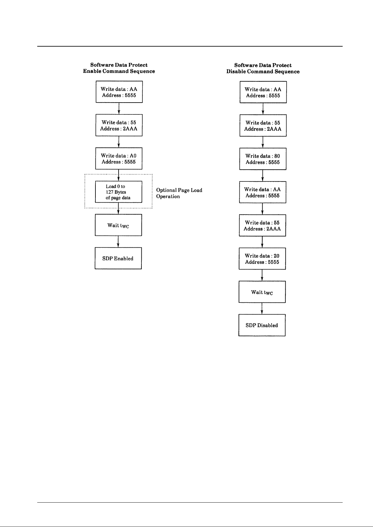
Figure 12 Software Data Protection Flowcharts
No. 5129-13/14
LE28C1001M, T-90/12/15
Page 14
No. 5129-14/14
LE28C1001M, T-90/12/15
Figure 13 Product ID Flowcharts Figure 14
Software Chip-Erase Flowchart
This catalog provides information as of November, 1997. Specifications and information herein are subject to
change without notice.
■ No products described or contained herein are intended for use in surgical implants, life-support systems, aerospace
equipment, nuclear power control systems, vehicles, disaster/crime-prevention equipment and the like, the failure of
which may directly or indirectly cause injury, death or property loss.
■ Anyone purchasing any products described or contained herein for an above-mentioned use shall:
➀ Accept full responsibility and indemnify and defend SANYO ELECTRIC CO., LTD., its affiliates, subsidiaries and
distributors and all their officers and employees, jointly and severally, against any and all claims and litigation and all
damages, cost and expenses associated with such use:
➁ Not impose any responsibility for any fault or negligence which may be cited in any such claim or litigation on
SANYO ELECTRIC CO., LTD., its affiliates, subsidiaries and distributors or any of their officers and employees
jointly or severally.
■ Information (including circuit diagrams and circuit parameters) herein is for example only; it is not guaranteed for
volume production. SANYO believes information herein is accurate and reliable, but no guarantees are made or implied
regarding its use or any infringements of intellectual property rights or other rights of third parties.
 Loading...