

Page 1
Quad intelligent power low side switch
■ Four low-side output driver with protection
diagnostics designed as a conventional switch
– 2 channels with 5 A output current
capability and r
– 2 channels with 3 A output current
capability and r
■ Integrated 60 V Zener diodes output clamping
structure
■ Output slope control
■ Short circuit protection
■ Open load detection in ON and OFF condition
■ Load bypass detection
■ Overload disable
■ Signal and power ground loss shutdown
■ Selective overtemperature shutdown
■ Electrostatic discharge (ESD) protection
Description
The L9349 is a monolithic IC designed to drive
inductive loads in low side configurations like
hydraulic valves used in ABS systems.
Particular care has been taken to protect the
device against failures, to avoid electromagnetic
interferences and to offer extensive real time
diagnostics.
The internal pull down current source at the
ENable and INput pins assures, that the device is
switched off, in case of open input conditions.
An output voltage slope limitation is implemented
to reduce the EMI.
Table 1. Device summary
Order code Package
= 0.2 Ω typ.
ON
= 0.3 Ω typ.
ON
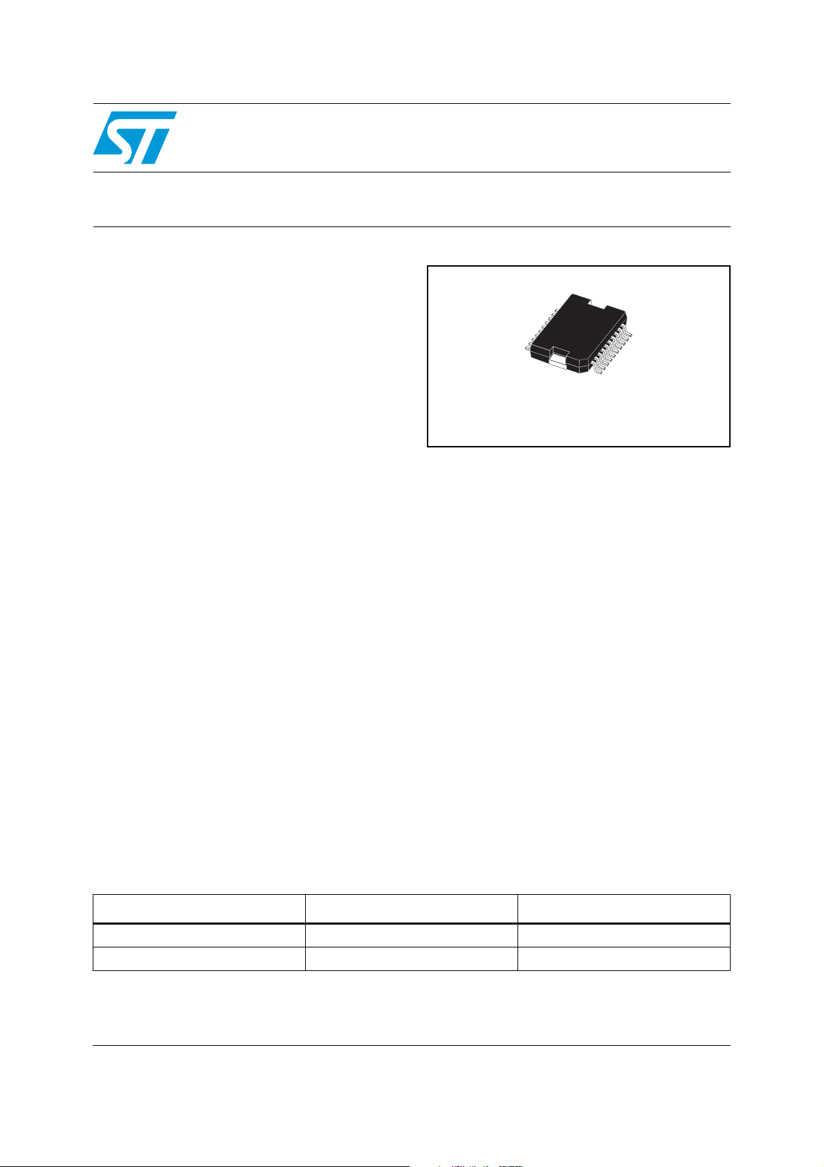
L9349-LF
PowerSO-20
The device is equipped with an integrated Zener
diodes clamp for fast inductive load current
recirculation. This structure limits the output
voltage during the recirculation phase to 50V.
The device is self-protected against short circuit
at the outputs and overtemperature.
For the real time error diagnosis, the voltage and
the current of the outputs are compared with
internally fixed thresholds to recognize open load
in OFF and ON conditions.
The output voltages are also compared with each
other in OFF condition with a fixed offset, in order
to recognize load bypasses.
If the over load current threshold is exceeded, the
output current will be limited internally during the
diagnostic overload delay switch-off time.
All four channels are monitored with a status
output. The diagnostic output level in connection
with different enable and input conditions allows it
to recognize the different fail states.
(1)
Packing
L9349-LF PowerSO-20 Tray
L9349TR-LF PowerSO-20 Tape and reel
1. ECOPACK® package (see Section 4: Package information)
September 2008 Rev 5 1/17
www.st.com
1
Page 2

Contents L9349-LF
Contents
1 Block diagram . . . . . . . . . . . . . . . . . . . . . . . . . . . . . . . . . . . . . . . . . . . . . . 5
2 Pins description . . . . . . . . . . . . . . . . . . . . . . . . . . . . . . . . . . . . . . . . . . . . 6
3 Electrical specifications . . . . . . . . . . . . . . . . . . . . . . . . . . . . . . . . . . . . . . 7
3.1 Absolute maximum ratings . . . . . . . . . . . . . . . . . . . . . . . . . . . . . . . . . . . . . 7
3.2 Thermal data . . . . . . . . . . . . . . . . . . . . . . . . . . . . . . . . . . . . . . . . . . . . . . . 7
3.3 Electrical characteristics (operating range) . . . . . . . . . . . . . . . . . . . . . . . . 8
3.4 Electrical characteristics . . . . . . . . . . . . . . . . . . . . . . . . . . . . . . . . . . . . . . . 8
3.5 Diagnostic . . . . . . . . . . . . . . . . . . . . . . . . . . . . . . . . . . . . . . . . . . . . . . . . . 10
3.6 Circuit description . . . . . . . . . . . . . . . . . . . . . . . . . . . . . . . . . . . . . . . . . . . 11
4 Package information . . . . . . . . . . . . . . . . . . . . . . . . . . . . . . . . . . . . . . . . 15
5 Revision history . . . . . . . . . . . . . . . . . . . . . . . . . . . . . . . . . . . . . . . . . . . 16
2/17
Page 3

L9349-LF List of tables
List of tables
Table 1. Device summary . . . . . . . . . . . . . . . . . . . . . . . . . . . . . . . . . . . . . . . . . . . . . . . . . . . . . . . . . . 1
Table 2. Pins description . . . . . . . . . . . . . . . . . . . . . . . . . . . . . . . . . . . . . . . . . . . . . . . . . . . . . . . . . . 6
Table 3. Absolute maximum ratings . . . . . . . . . . . . . . . . . . . . . . . . . . . . . . . . . . . . . . . . . . . . . . . . . . 7
Table 4. Thermal data. . . . . . . . . . . . . . . . . . . . . . . . . . . . . . . . . . . . . . . . . . . . . . . . . . . . . . . . . . . . . 7
Table 5. Electrical characteristics (operating range). . . . . . . . . . . . . . . . . . . . . . . . . . . . . . . . . . . . . . 8
Table 6. Electrical characteristics . . . . . . . . . . . . . . . . . . . . . . . . . . . . . . . . . . . . . . . . . . . . . . . . . . . . 8
Table 7. Diagnostic . . . . . . . . . . . . . . . . . . . . . . . . . . . . . . . . . . . . . . . . . . . . . . . . . . . . . . . . . . . . . . 10
Table 8. Corresponding filter time for each detected signal . . . . . . . . . . . . . . . . . . . . . . . . . . . . . . . 11
Table 9. Document revision history . . . . . . . . . . . . . . . . . . . . . . . . . . . . . . . . . . . . . . . . . . . . . . . . . 16
3/17
Page 4

List of figures L9349-LF
List of figures
Figure 1. Block diagram . . . . . . . . . . . . . . . . . . . . . . . . . . . . . . . . . . . . . . . . . . . . . . . . . . . . . . . . . . . . 5
Figure 2. Pins connection (top view) . . . . . . . . . . . . . . . . . . . . . . . . . . . . . . . . . . . . . . . . . . . . . . . . . . 6
Figure 3. t
Figure 4. Output slope (resistive load for testing) . . . . . . . . . . . . . . . . . . . . . . . . . . . . . . . . . . . . . . . 12
Figure 5. Timing (t
Figure 6. Block diagram - Open load voltage detection . . . . . . . . . . . . . . . . . . . . . . . . . . . . . . . . . . . 13
Figure 7. Logic diagram . . . . . . . . . . . . . . . . . . . . . . . . . . . . . . . . . . . . . . . . . . . . . . . . . . . . . . . . . . . 14
Figure 8. Application circuit diagram . . . . . . . . . . . . . . . . . . . . . . . . . . . . . . . . . . . . . . . . . . . . . . . . . 14
Figure 9. PowerSO-20 mechanical data and package dimensions . . . . . . . . . . . . . . . . . . . . . . . . . . 15
clamping time . . . . . . . . . . . . . . . . . . . . . . . . . . . . . . . . . . . . . . . . . . . . . . . . . . . . . . . . 12
EO
, t
DOL
). . . . . . . . . . . . . . . . . . . . . . . . . . . . . . . . . . . . . . . . . . . . . . . . . . . . . . . 13
DIOU
4/17
Page 5
L9349-LF Block diagram
1 Block diagram
Figure 1. Block diagram
IN1
D1
EN
IN4
D4
IN2
D2
IN3
D3
00AT0025
Output Control
Diagnostic
Control
R
QS
Channel 1
Delay
Time
Channel 4
Channel 2
Channel 3
GND
Overtemp
Overload
Openload
52V
OUT1
VS
OUT4
R
IO
OUT2
OUT3
5/17
Page 6
Pins description L9349-LF
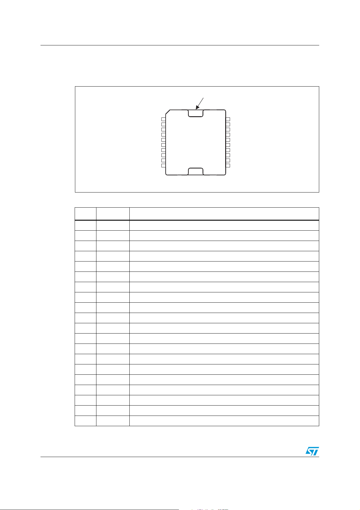
2 Pins description
Figure 2. Pins connection (top view)
Heat sink connected
to pins 1, 10, 11, 20
PGND 1
OUT1 2
D1
3
IN4 4
VS 5
NC
6
IN3 7
D2 8
OUT2
PGND 10
00AT0026
Table 2. Pins description
9
N° Pin Function
1 PGND Power Ground
2 Out1 Output 1 (5A)
3 D1 Diagnostic 1
4IN4Input 4
5 VS Supply Voltage
6 NC Not Connected
7IN3Input 3
20 PGND
OUT4
19
D418
IN117
EN
16
GND15
IN214
13
D3
OUT312
PGND11
8 D2 Diagnostic 2
9 Out2 Output 2 (5A)
10 PGND Power Ground
11 PGND Power Ground
12 Out3 Output 3 (3A)
13 D3 Diagnostic 3
14 IN2 Input 2
15 GND Signal Ground
16 EN Common Enable
17 IN1 Input 1
18 D4 Diagnostic 4
19 Out4 Output 4 (3A)
20 PGND Power Ground
6/17
Page 7

L9349-LF Electrical specifications
3 Electrical specifications
3.1 Absolute maximum ratings
Table 3. Absolute maximum ratings
Symbol Parameter Conditions Value Unit
V
⎪dV
V
IN, EN
V
I
O1, 2
I
O3, 4
I
OR1, 2
I
OR3, 4
E
E
Δ
T
V
V
ODC
O1, 2
O3, 4
V
DC supply voltage -0.3 to 32 V
S
Supply voltage pulse
SP
(duration <200ms)
/dt⎪ Supply voltage slope 10
S
Input voltage ⎪I⎪
Diagnostic DC output voltage ⎪I⎪ 50mA -0.3 to 16 V
D
10mA
DC output voltage -0.3 to 45 V
DC output current out 1, 2
DC output current out 3, 4
internal limited (Max.)
internal limited (Max.)
Reverse output current -5 A
Reverse output current -3 A
= 250μs,
t
Switch-off energy for inductive
loads
GND potential difference Tj = -40 to 150°C ±0.3 V
GND
Junction temperature during switch-
jEO
off
EO
T = 5ms 30 mJ
Σt ≤ 30 min 175 °C
Σt ≤ 15 min 190 °C
(1)
-0.3 to 45 V
V/μs
-1.5 to 6 V
>5 (Min.)
>3 (Min.)
50 mJ
A
A
T
Junction temperature -40 to T
j
T
T
jDIS
Storage temperature -55 to 150 °C
stg
Thermal disable junction
temperature threshold
ESD Electrostatical discharging MIL883C +-2 kV
ESD OUT1 - 4
1. tEO is the clamping time (see Figure 3)
3.2 Thermal data
Table 4. Thermal data
Symbol Parameter Value Unit
R
Th j-case
Thermal resistance junction to case 3 °C/W
jDIS
°C
180 to 210 °C
vs. Common-GND
(PGNDs + GND)
+-4 kV
7/17
Page 8

Electrical specifications L9349-LF
3.3 Electrical characteristics (operating range)
The electrical characteristics are valid within the below defined operating range, unless
otherwise specified.
Table 5. Electrical characteristics (operating range)
Symbol Parameter Test Condition Min. Typ. Max. Unit
V
S
T
j1
T
j2
1. Parameters guaranteed by correlation
Board supply voltage 4.5 12 32 V
-40 150 °C
Junction temperature
Σt ≤ 15min
(1)
over life time 150 T
jDIS
°C
3.4 Electrical characteristics
Table 6. Electrical characteristics
(VS = 4.5 to 32V; -40°C ≤ Tj1 ≤ 150°C < Tj2 ≤ T
Symbol Parameter Test conditions
Supply
I
VS OFF
I
VS ON
Diagnostic outputs D1 - D4
V
DL
I
DLE
Outputs Out 1 - Out 4
R
DSON 1, 2
R
DSON 3, 4
V
R
V
OUV 1-4
DC supply current Off EN = 1.0V 5 10 mA
DC supply current On VS ≤ 14V; VIN, VEN = 2V 8 mA
Diagnostic output low
voltage
Diagnostic output
leakage current
Output On resistance
Z-diode clamping
Z
voltage
Output pull down
O
resistor
Open load voltage
threshold
≤ 3mA 0.65 1.0 1.5 V
I
D
(1)
= 14V
V
D
T
= 25°C
j
= 150°C
T
j
> 9.5V I
V
S
O1,2
Tj = 25°C
= 150°C
T
j
> 9.5V
V
S
I
= 1.3A
O3,4
≥ 200mA 45 60 V
I
OCL
VS > 9.5V
EN = 0V
= 1V
V
IN
= 2A
, unless otherwise specified.)
jDIS
Values T
j1
Values T
j2
Min. Typ. Max. Min. Max.
0.1 2 20 μA
200
300
300
500
450
750
10 40 50 k
0.525 x
V
0.55 x
S
0.575 x
V
S
V
S
Unit
m
m
Ω
V
Ω
Ω
8/17
Page 9

L9349-LF Electrical specifications
Table 6. Electrical characteristics (continued)
(VS = 4.5 to 32V; -40°C ≤ Tj1 ≤ 150°C < Tj2 ≤ T
Symbol Parameter Test conditions
, unless otherwise specified.)
jDIS
Values T
j1
Values T
Min. Typ. Max. Min. Max.
j2
Unit
V
OUV hys 1-4
ΔV
OUV 1-4,
2-3, 4-1, 3-2
ΔV
OUV hys 1-
4, 2-3,
4-1, 3-2
I
OUC 1, 2, 3, 4
I
OOC 1, 2
I
OOC 3, 4
T
SD
T
SD-hys
I
OUT-LE
Hysteresis
Open load difference
voltage threshold
Open load hysteresis 40 mV
Open load current
threshold
Over load current
threshold
Thermal shut down 180 195 210 °C
Thermal shut down
hysteresis
OUT leakage current
Inputs IN1-4, EN
IN1,4/2,3
= 1V VS ≤
V
16V
≥ 4.5V
V
Oc
= output voltage of
V
OC
other channel
VEN=VIN=2V;
=6.5 - 16V
V
S
VS > 6.5V;
V
= 32V
OUT
V
= 20V
OUT
= 0V
V
S
V
OC
1.0V
-
0.003 x
V
S
V
-
OC
1.25V
V
OC
1.5V
-
V
V
160 320 480 mA
510 A
36 A
20 °C
5
μA
V
IN,EN L
V
IN,EN H
V
EN,IN hys
I
I
EN
Timing
t
ON
t
t
OFF
Logic input/enable low
voltage
Logic input/enable
high voltage
IN, EN 2.0 6 V
-0.3 1 V
Logic input hysteresis 50 100 mV
IN
Input sink current
Enable sink current 10 20 40 μA
Output delay ON time
f,r
Output fall and rise
time
Output delay OFF
time
2V < V
, VEN < 6V
IN
VIN, VEN < V
I
= 1A
O
= 12V
V
S
(3)
Figure 4
= 1A
I
O
= 12V
V
S
Figure 4
= 1A
I
O
V
= 12V
S
(3)
Figure 4
s
(2)
10 20 40 μA
425
31030 μs
51530
μs
μs
9/17
Page 10

Electrical specifications L9349-LF
Table 6. Electrical characteristics (continued)
(VS = 4.5 to 32V; -40°C ≤ Tj1 ≤ 150°C < Tj2 ≤ T
Symbol Parameter Test conditions
, unless otherwise specified.)
jDIS
Values T
j1
Values T
Min. Typ. Max. Min. Max.
j2
Unit
t
DH-L, Diag
t
D IOU
t
DOL
t
filt
Diag. delay output
OFF time
Diagnostic open load
delay time
Diagnostic overload
delay switch-OFF time
Filter time 4 24 μs
(3)
Figure 4 86590μs
9V< VS <16V, Figure 5 850 μs
9V< VS <16V, Figure 5 665 μs
PGND
PGND
PGND
1. The diagnostic output is short circuit protected up to VD = 16V
2. Open pins (EN, IN) are detected as low
= 9 to 16V ∧ I
3. V
S
Power GND loss
loss,h
threshold high
Power GND loss
loss,l
threshold low
OUC
≤ IO ≤ I
OOC
3.5 Diagnostic
Table 7. Diagnostic
Conditions EN IN OUT DIAG.
3V
2V
Normal function
GND short V
Load bypass
Open load I
≥ 190°C Overtemperature X X off L
T
jtyp
Over load
< 0.55VS L X off H
Otyp
ΔV
O1,2,3,4typ
I
Omin 1,2
I
Omin 3,4
≥ 1.25V H L off H
O1-4/2-3
< 320mA H H on L
> 5A
> 3A
SGND or PGND loss channel off X L off H
SGND or PGND loss channel on H H off L
10/17
LXoffL
HLoffL
HHonH
HHoffL
Page 11

L9349-LF Electrical specifications
3.6 Circuit description
The L9349 is a quad low side driver for inductive loads like valves in automotive
environment. The internal pull down current sources at the ENable and INput pins assure in
case of open input conditions that the device is switched off. An output voltage slope
limitation for du/dt is implemented to reduce the EMI. An integrated active flyback voltage
limitation clamps the output voltage during the flyback phase to 50 V.
Each driver is protected against short circuit at V
circuit condition the output will be disabled after a short delay time t
for T
> 180°C of the output will be reset if the junction temperature decreases about 20°C
J
< 32V and thermal overload. In short
OUT
. The thermal disable
DOL
below the disable threshold temperature.
The overtemperature, overload and groundloss information is stored until IN is low.
For the real time error diagnosis the voltage and the current of the outputs are compared
with internal fixed values V
(R
≥ 20KΩ, RL > 38Ω) in OFF and ON conditions.
L
Also the output voltages V
fixed offset of
ΔV
to recognize load bypasses. The ΔV
OUV
for OFF and I
OUV
are compared to each other output in OFF condition with a
O1- 4
for ON conditions to recognize open load
OUC
diagnoses is suppressed
OUV
during the flyback phases of the compared output. The outputs 1 and 4 are compared for
ΔV
and also outputs 2 and 3 are compared.
OUV
The diagnostic output level in connection with different ENable and INput conditions allows
to recognize different fail states, like overtemp, short to V
, short to GND, bypass to GND
S
and disconnected load (see Table 7: Diagnostic).
The diagnostic output is protected against short circuit. Exceeding the over load current
threshold I
delay switch-off time t
The device complies the I
, the output current will be limited internally during the diagnostic overload
OOC
.
DOL
pulses imposed to the supply voltage of the valves without any
SO
failures of the functionality. Therefore some diagnostic functions are internal filtered. The
following table shows the corresponding filter time for each detected signal.
Table 8. Corresponding filter time for each detected signal
ON State
EN and IN =
HIGH
Overloading of output
(also shorted load to supply)
Open load
(under voltage detection)
Open load
(under current detection)
Overtemperature X 4
Power-signal GND-loss X 4
Power-signal GND-loss X 4
Openload difference X 4
X4
X-
OFF State
EN or IN,
= LOW
X-
11/17
Filter
min.
Reset done by
time
μsINx = “LOW”
μsINx = “LOW”
μsINx = “LOW”
μs
μs
Page 12

Electrical specifications L9349-LF
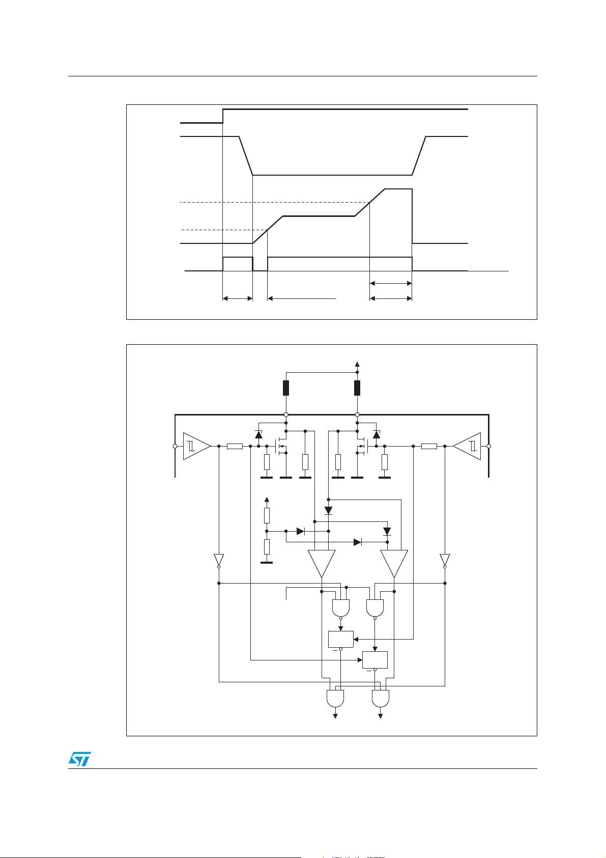
Figure 3. tEO clamping time
V
O1-4
V
OCL
V
S
t
EO
t
T
00AT0027
Figure 4. Output slope (resistive load for testing)
V
IN
V
EN
5V
V
H
V
L
V
OUT
t
ON
t
OFF
t
V
0.85V
V
OUV
0.15V
V
DIAG
V
0.5V
00AT0030
S
S
S
t
t
f
D
D
t
D H-L Diag
t
r
12/17
Page 13
L9349-LF Electrical specifications
Figure 5. Timing (t
DOL
, t
DIOU
)
IN
V
ON
I
OOC
I
OUC
V
D
00AT0032
t
DIOU
Open Load Current
t
t
DOL
filt
Figure 6. Block diagram - Open load voltage detection
V
Batt
(L2) L4 (L3)
L
OUT1
(OUT2)
1
OUT4
(OUT3)
IN
1
00AT0033
V
S
55%
Enable
IN
4
R
IO
R
IO
±
+
R
Latch
S
Q
S
Latch
+
±
R
Q
VO
UV1
VO
UV4
13/17
Page 14
Electrical specifications L9349-LF
Figure 7. Logic diagram
V
EN
V
IN
VO
U
IO
O
IO
U
V
D
Normal
Operation ON
00AT0034
Open Load Current
Open Load Current
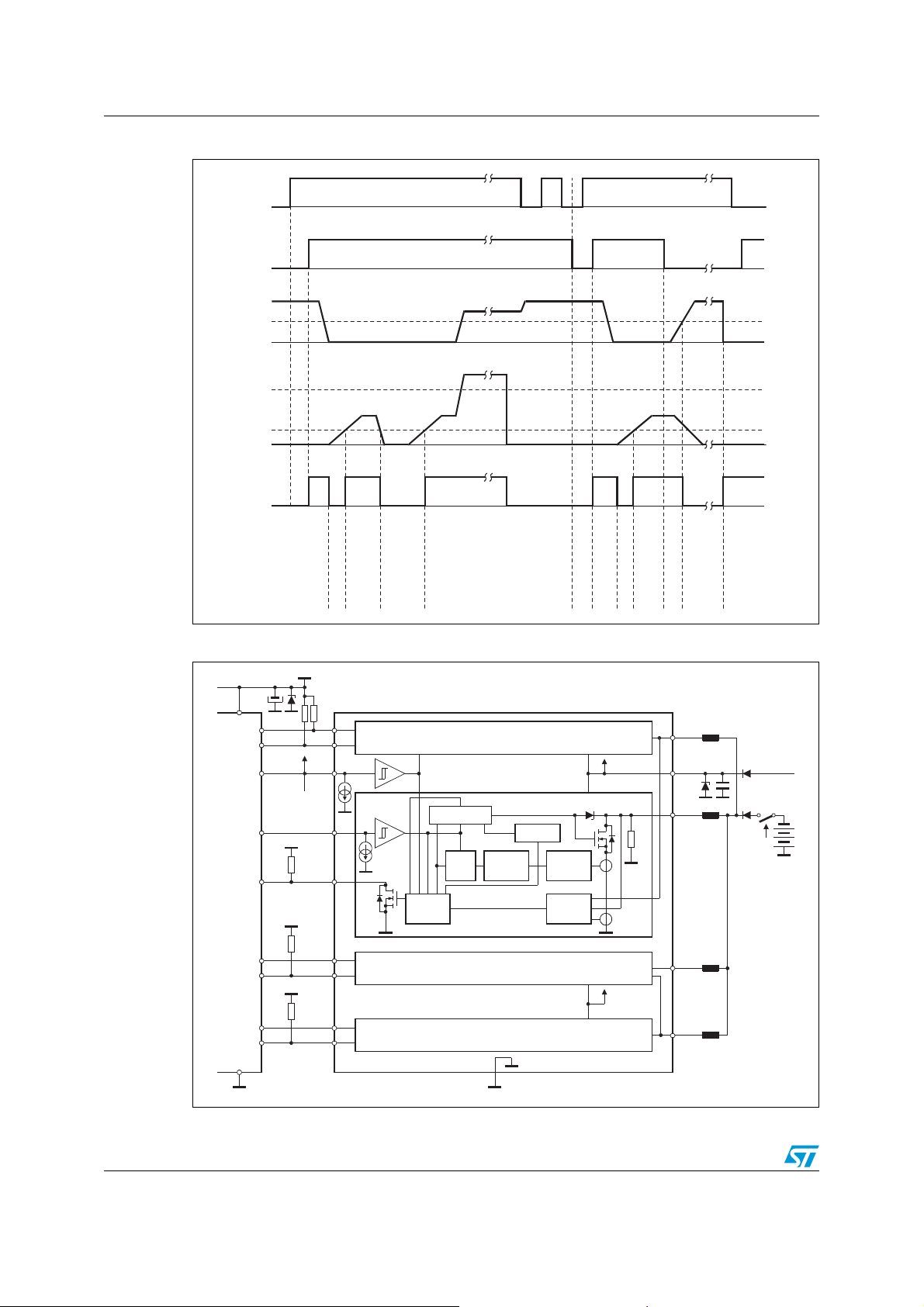
Figure 8. Application circuit diagram
+5V
V
CC
+5V
+5V
+5V
IN1
IN4I/O
IN2
D1
EN
Output Control
R
Diagnostic
Control
QS
D4I/O
D2
μ
P
Controller
I/O
I/O
I/O
I/O
I/O
Channel 1
Delay
Time
Channel 4
Channel 2
Latched
Overtemp
Over. Load
Diagnostic
Overload
Openload
Latch Reset
Open Load Current
52V
Normal
R
IO
Operation ON
Open Load Voltage
OUT1
VS
+45V
OUT4
OUT2
Normal
Operation OFF
Z
VALVE
Z
VALVE
Z
VALVE
V
Batt
Open Load Voltage
KL15
KL30
I/O
I/O
GND GND
00AT0035
IN3
D3
14/17
Channel 3
OUT3
Z
VALVE
Page 15

L9349-LF Package information
4 Package information
In order to meet environmental requirements, ST (also) offers these devices in ECOPACK®
packages. ECOPACK
®
packages are lead-free. The category of second Level Interconnect
is marked on the package and on the inner box label, in compliance with JEDEC Standard
JESD97. The maximum ratings related to soldering conditions are also marked on the inner
box label.
ECOPACK is an ST trademark. ECOPACK specifications are available at: www.st.com.
Figure 9. PowerSO-20 mechanical data and package dimensions
DIM.
A3.60.142
a1 0.1 0.3 0.004 0.012
a2 3.3 0.130
a3 0 0.1 0.000 0.004
b 0.4 0.53 0.016 0.021
c 0.23 0.32 0.009 0.013
D (1) 15.8 16 0.622 0.630
D1 (2
) 9 .4 9.8 0.370 0.386
E 13.9 14.5 0.547 0.570
e 1.27 0.050
e3 11.43 0.450
E1 (1) 10.9 11.1 0.429 0.437
E2 2.9 0.114
E3 5.8 6.2 0.228 0.244
G 0 0.1 0.000 0.004
H 15.5 15.9 0.610 0.626
h 1.1 0.043
L 0.8 1.1 0.031 0.043
N 8˚(typ.)
S 8˚(max. )
T 10 0 .394
(1) “D and E1” do n ot include mold flash or protusion s.
- Mold flash or pr otusions shal l not exceed 0.1 5mm (0.006”)
- Critical dim ensions: “E”, “G” and “a3”.
(2)
For subcontractors, the limit is the one quoted in jedec MO-166
mm inch
MIN. TYP. MAX. MIN. TYP. MAX.
OUTLINE AND
MECHANICAL DATA
Weight: 1.9gr
JEDEC MO-166
PowerSO-20
NN
b
DETAIL A
e3
H
D
E2
T
110
h x 45˚
R
a2
A
e
1120
E1
DETAIL B
PSO20MEC
lead
a3
Gage Plane
BOTTOM VIEW
E
DETAIL B
0.35
S
D1
L
a1
DETAIL A
c
slug
- C -
SEATING PLANE
GC
(COPLANARITY)
E3
0056635 I
15/17
Page 16

Revision history L9349-LF
5 Revision history
Table 9. Document revision history
Date Revision Changes
20-Sep-2002 4 Initial release.
Document reformatted.
09-Sep-2008 5
Updated feature and description on page 1.
Added Table 1: Device summary on page 1.
Updated Table 3: Absolute maximum ratings on page 7.
16/17
Page 17

L9349-LF
Please Read Carefully:
Information in this document is provided solely in connection with ST products. STMicroelectronics NV and its subsidiaries (“ST”) reserve the
right to make changes, corrections, modifications or improvements, to this document, and the products and services described herein at any
time, without notice.
All ST products are sold pursuant to ST’s terms and conditions of sale.
Purchasers are solely responsible for the choice, selection and use of the ST products and services described herein, and ST assumes no
liability whatsoever relating to the choice, selection or use of the ST products and services described herein.
No license, express or implied, by estoppel or otherwise, to any intellectual property rights is granted under this document. If any part of this
document refers to any third party products or services it shall not be deemed a license grant by ST for the use of such third party products
or services, or any intellectual property contained therein or considered as a warranty covering the use in any manner whatsoever of such
third party products or services or any intellectual property contained therein.
UNLESS OTHERWISE SET FORTH IN ST’S TERMS AND CONDITIONS OF SALE ST DISCLAIMS ANY EXPRESS OR IMPLIED
WARRANTY WITH RESPECT TO THE USE AND/OR SALE OF ST PRODUCTS INCLUDING WITHOUT LIMITATION IMPLIED
WARRANTIES OF MERCHANTABILITY, FITNESS FOR A PARTICULAR PURPOSE (AND THEIR EQUIVALENTS UNDER THE LAWS
OF ANY JURISDICTION), OR INFRINGEMENT OF ANY PATENT, COPYRIGHT OR OTHER INTELLECTUAL PROPERTY RIGHT.
UNLESS EXPRESSLY APPROVED IN WRITING BY AN AUTHORIZED ST REPRESENTATIVE, ST PRODUCTS ARE NOT
RECOMMENDED, AUTHORIZED OR WARRANTED FOR USE IN MILITARY, AIR CRAFT, SPACE, LIFE SAVING, OR LIFE SUSTAINING
APPLICATIONS, NOR IN PRODUCTS OR SYSTEMS WHERE FAILURE OR MALFUNCTION MAY RESULT IN PERSONAL INJURY,
DEATH, OR SEVERE PROPERTY OR ENVIRONMENTAL DAMAGE. ST PRODUCTS WHICH ARE NOT SPECIFIED AS "AUTOMOTIVE
GRADE" MAY ONLY BE USED IN AUTOMOTIVE APPLICATIONS AT USER’S OWN RISK.
Resale of ST products with provisions different from the statements and/or technical features set forth in this document shall immediately void
any warranty granted by ST for the ST product or service described herein and shall not create or extend in any manner whatsoever, any
liability of ST.
ST and the ST logo are trademarks or registered trademarks of ST in various countries.
Information in this document supersedes and replaces all information previously supplied.
The ST logo is a registered trademark of STMicroelectronics. All other names are the property of their respective owners.
© 2008 STMicroelectronics - All rights reserved
STMicroelectronics group of companies
Australia - Belgium - Brazil - Canada - China - Czech Republic - Finland - France - Germany - Hong Kong - India - Israel - Italy - Japan -
Malaysia - Malta - Morocco - Singapore - Spain - Sweden - Switzerland - United Kingdom - United States of America
www.st.com
17/17
 Loading...