

■
SUPPLY VOLTAGE RANG E: 4. 8 TO 18V
■
OUTPUT VOLTAGE UP TO 40V
■
OUTPUT VOLTAGE CLAMP DURING
RECIRCULATION OF INDUCTIVE LOADS
■
OUTPUT CURRENT CAPABIL ITY 2 X 5A AND
2 X 3A
■
LOW POWER DISSIPATION DURING
RECIRCULATION OF INDUCTIVE LOADS BY
INTEGRATED FREE WHEELING DIODES
(3A-DRIVER S ONLY)
■
LOW ON-RESISTANCE 2 X 0.2Ω , 2 X 0.35Ω (TYP.)
■
OUTPUT SHORT CIRCUIT CURRENT
PROTECTION
■
REAL TIME DIAGNOSTIC FUNCTIONS
■
OVERTEMPERATURE SHUTDOWN
■
SIGNAL- AND POWER-GROUND-LOSS
SHUTDOWN
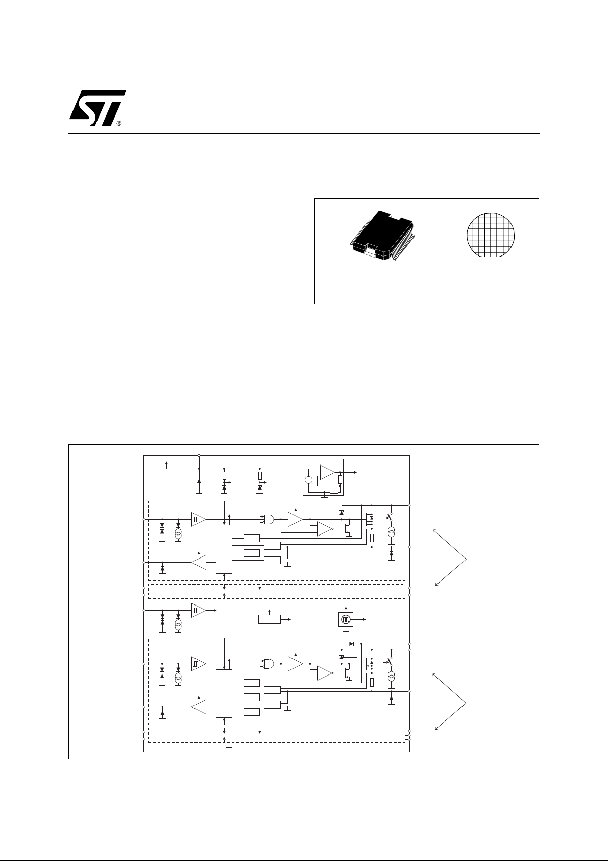
L9348
QUAD LOW SIDE DRIVER
PowerSO-36 BARE DIE
ORDERING NUMB ERS :
L9348 L9348-DIE1
■
3.3V CMOS COMPATIBLE INPUTS AND
STATUS
DESCRIPTION
The L9348 is a monolithic integrated quad low side
driver realized in advanced Multipower-BCD technology. It is intended to drive inductive loads (relays,
electromagnetic valves) in automotive and industrial
applications.
Figure 1. Block Diagram
V
S
IN1
ST1
IN2
ST2
ENA
IN3
ST3
IN4
ST4
99AT0073
March 2002
VS
C 166kHz
V
DD
V
REG
Diagnostic
PWRES
C 166kHz EN
PWRES
EN
C 166kHz
V
DD
V
REG
Diagnostic
PWRES
C 166kHz EN
PWRES
GND
Voltage Regulator
+
–
=
V
S
≥
1
PWRES C 166kHz
V
S
≥
1
TSD
TSD
V
CC
EN
OL
SCP
GL
V
DD
PWRES
EN
OL
SCP
GL
FB
V
DD
FAIL
FAIL
VREG
Q1
EN
PGND1
5A - DRIVER
CHANNEL1
CHANNEL2
V
S
EN
CHANNEL3
CHANNEL4
Q2
PGND2
D3
Q3
PGND3
D4
Q4
PGND4
3A - DRIVER
1/13
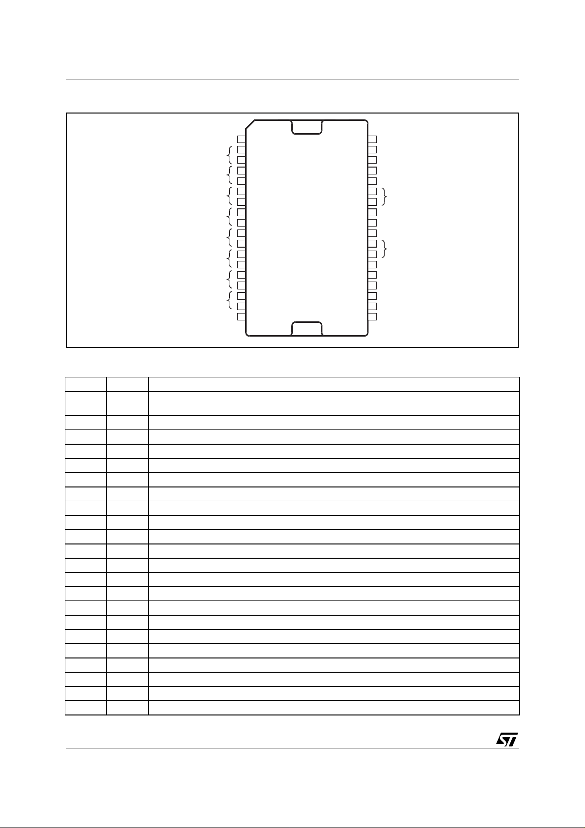
L9348
Figure 2. Pin Connection
N.C.
PGND3
Q3
D3
Q1
Q2
D4
Q4
PGND4
N.C.
99AT0074
1
2
3
4
5
6
7
8
9
10
11
12
13
14
15
16
17
18
Table 1. Pin Description
N° Pin Function
1, 18,
19, 36
2, 3 PGND3 Power Ground Channel 3
4, 5 Q3 Power Output Channel 3 (3A switch)
6, 7 D3 Recircula tion Diode Chan nel 3
8, 9 Q1 Power Output Channel 1 (5A switch)
10, 11 Q2 Power Output Channel 2 (5A switch)
12, 13 D4 Recircula tion Diode Chan nel 4
14, 15 Q4 Power Output Channel 4 (3A switch)
16, 17 PGND4 Power Ground Channel 4
20 ST4 Status Output Channel 4
21 IN2 Control Input Channel 2
22 IN4 Control Input Channel 4
23 ST2 Status Output Channel 2
24 ENA Enable
25, 26 PGND2 Power Ground Channel 2
27 GND Signal Ground
28 VS Supply Voltage
29 N.C. Not Connected
30, 31 PGND1 Power Output Channel 3
32 ST1 Status Output Channel 1
33 IN3 Control Input Channel 3
34 IN1 Control Input Channel 1
N.C. (GND)
36
35
34
33
32
31
30
29
28
27
26
25
24
23
22
21
20
19
N.C.
ST3
IN1
IN3
ST1
PGND1
N.C.
VS
GND
PGND2
ENA
ST2
IN4
IN2
ST4
N.C.
2/13
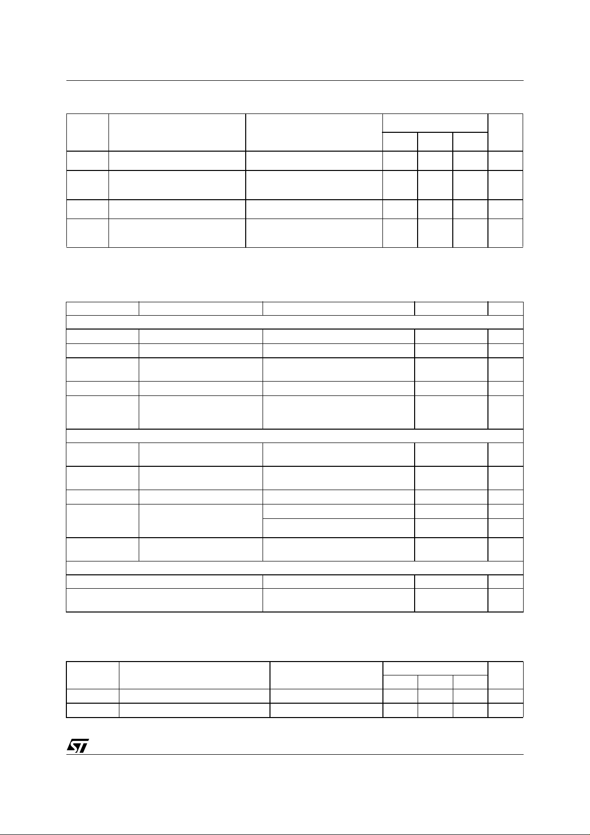
Table 2. Thermal Data
Symbol Parameter Test Conditions
T
Junction temperature -40 150 °C
j
L9348
Values
Unit
Min. Typ. Max.
T
T
R
th j-case
Junction temperature during
jc
clamping (life time)
Storage temperature -55 150 °C
stg
t = 30min
Σ
t = 15min
Σ
Thermal resistance junction to
175
190
2 °C/W
°C
°C
case
Table 3. Absolute Maximum Ratings
The absolute maximum ratings are the limiting values for this device. Damage may occur if this device is
subjected to conditions which are beyond these values
Symbol Parameter Test Conditions Value Unit
Voltages
V
S
V
, V
Q
D
, V
V
IN
EN
V
ST
V
DRmax
Currents
I
Q 1/2
I
Q 3/4
I
ST
E
Q1/2
I
FDmax
ESD Protection
Supply and Signal pins versus GND ±2kV
Output pins (Q
Supply voltage range -0.3 to 40 V
max. static Output voltage 40 V
Input voltage range
|II | < 10mA -1.5 to 6 V
(IN1 to IN4, EN)
Status output voltage range |II | < 1mA -0.3 to 6 V
max. Reverse breakdown
= 100 µA
I
R
voltage free wheeling diodes
D3, D4
Output current at reversal
supply for Q1, Q2
Output current at reversal
supply for Q3, Q4
Status output current range -1 to 1 mA
max. Discharging energy for
inductive loads per channel
Q1, Q2
max. load current free
= 25°C 50 mJ
T
j
T
= 150°C 30 mJ
j
t < 5ms 3 A
wheeling diodes
, DX) versus common ground (=short of
X
.
55 V
-4 A
-2 A
±4kV
SGND with all PGND)
Note: Human Body Model according to MIL883C. The device withstands ST1 class level.
Table 4. Operating Range
.
Symbol Parameter Test Conditions
V
S
T
Supply voltage 4.8 18 V
Junction temperature -40 150 °C
j
Values
Min. Typ. Max.
Unit
3/13
L9348
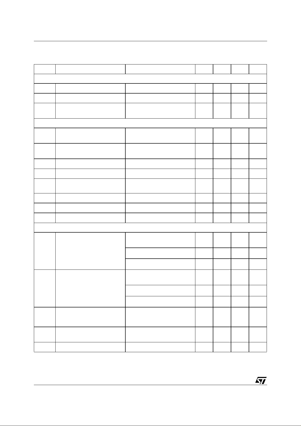
Table 5. Electrical Characteristcs
The electrical characteristics are valid within the operating range
Symbol Parameter Test Condition Min. Typ. Max. Unit
Power Supply
I
Supply current V
S
I
Quiescent current (outputs OFF) V
Q
IN1...IN4, ENA
= L 6 mA
ENA
= H 8 mA
(Table 4)
, unless otherwise specified
I
D3/4
Quiescent current at pins D3/4
Diagnostic Functions
V
QU1 to 4
Output open load voltage
threshold
I
QU1 to 4
Output open load current
threshold
I
QO1/2
I
QO3/4
Overload current threshold Q 1, 2
Overload current threshold Q 3, 4
TthOvertemperature shutdown
threshold
V
V
T
thPGL
thSGL
Overtemperature hysteresis 10 °C
hy
Power-GND-loss threshold 1.5 2.5 3.5 V
Signal-GND -loss thresh old 150 330 510 mV
Power Outputs (Q1 to Q4)
R
DSON1/2
Static drain-source ON-resistance
Q1, Q2
≤ 18V;
V
D3/4
V
= L
IN3/4
≥ 6.5V
V
S
VEN = X; VIN = L
≥ 6.5V
V
S
VEN = H; VIN = H
≥ 6.5V
V
S
≥ 6.5V
V
S
2)
= 1A; VS ≥ 9.5V
I
Q
Tj = 25°C
Tj = 125°C
3)
10 400
0.3 0.33 0.36 x V
A
µ
S
50 140 mA
57.59 A
358A
175 210 °C
0.2
0.5
Ω
Ω
R
DSON3,4
V
Z
V
C
I
PD
4/13
Static drain-source ON-resistance
Q3, Q4
Z-diode clamping voltage
= threshold of flyback detection
Q3/4
Clamping voltage
Output pull down current V
Tj = 150°C
= 1A; VS ≥ 9.5V
I
Q
T
= 25°C
j
T
= 125°C
j
T
= 150°C
j
≥ 100mA,
I
Q
pos. supply V
≥ 100mA,
I
Q
neg. supply V
ENA
4)
0.35 Ω
3)
4)
45 60 V
D3/4
410V
D3/4
= H, VIN = L 10 20 50
0.5
0.75 Ω
0.75 Ω
µ
Ω
A

L9348
Table 5. Electrical Characteristcs
The electrical characteristics are valid within the operating range
Symbol Parameter Test Condition Min. Typ. Max. Unit
(Table 4)
, unless otherwise specified
V
I
FD3/4
Output leakage current V
Qlk
Forward voltage of
free wheeling diodes D3, D4
R
Gate pull down resistor for
PD0
nonsupplied V
S
Timings
t
t
OFF
t
DSO
t
filter
t
OLOFF
Output ON delay time
ON
t
Output ON fall time
f
Output OFF delay time
t
Output OFF rise time
r
Overload switch-OFF delay time 6 30 65
t
Output OFF status delay time 0.75 1.5 2.25 ms
D
error detection filter time
OLOFF error detection filter time 20 70
Digital Inputs (IN1 to IN4, ENA)
= L,Tj = 25°C 1
ENA
T
= 125°C 5
j
I
= -1.5A 0.5 1.75 V
D3/4
VS = 0V,
≥ 6.5V
V
D3/4
= 1A
I
Q
IQ = 1A
IQ = 1A
IQ = 1A
2)
1)
1)
1)
1)
0.3 3 kΩ
0520
0.5 1.5 8
01030
0.5 1.5 5
5.8 35
A
µ
A
µ
s
µ
s
µ
s
µ
s
µ
s
µ
s
µ
s
µ
V
V
V
I
Input low voltage -1.5 1 V
IL
Input high voltage 2 6 V
IH
Input voltage hysteresis
IHy
Input pull down current
IN
2)
= 5V, VS ≥ 6.5V
V
IN
50 100 mV
82040
Digital Outputs (ST1 to ST4)
V
V
R
DIAGLROUT
R
DIAGHROUT
Status output voltage in low state
STL
5)
Status output voltage in high state
STH
5)
+ R
+ R
chapter 2.0 Timing Di ag rams
(1).See
(2).This parameter will not be tested but assured by design
(3).Wafer-measurement
(4).Measured on P-SO36 devices
(5).Short circuit between two d i gi tal output s (one in high th e other in low st ate) will lea d to the define d result "LO W"
in low state 0.3 0.64 1.5
DSON
in high state 1.5 3.2 7
DSON
IST ≤ 40µA
IST ≥ -40µA
≥ -120µA
I
ST
; resistive load condition; VS ≥ 9V
0 0.4 V
2.5 3.45 V
23.45V
A
µ
k
Ω
k
Ω
5/13

L9348
1.0 FUNCTIONAL DESCRIPTION
1.1 Overview
The four low-side switches are designed to drive inductive loads (relays, electromagnetic valves). For the 3A
switches (Q3/4) integrated free-wheeling diodes (D3/4) are available and can be used as recirculation path for
inductive loads. If either integrated nor external free-wheeling diodes are used the output voltage is clamped
internally during discharge of inductive loads. The switches are controlled by CMOS compatible inputs (IN1-4)
if the enable input is set to “high”. The status of each switch is monitored by the related status output (ST1-4).
1.2 Input Circuit s
The control and enable inputs are activ e high, featur ing switching thr es holds with hy ster esis and pull-dow n current sources. Not c onnected i nputs are i nter preted as “LO W”. If the enable input i s set to “LOW” the output s are
switched off independent of the control input state (IN1-4).
1.3 Switching Stages
The four power outputs consist of DMOS-power transistors. The output stages are protected against short ci rcuit
to supply. Integrated output voltage clamp limits the output voltage in case of inductive load current flyback. Internal pull down current sources are provided at the outputs to assure a defined conditon in OFF mode. They
will be disconnected in the disable mode (ENA=L). If the supply of the device gets lost but the loads and D3/4
are still supplied, an internal pull down resistor discharges the gate of the DMOS-power transistor to avoid
switch on due to capacitive coupling.
1.4 Status O u t puts
The CMOS compatible status outputs indicate the state of the drivers (LOW-level indicates driver in OFF state,
HIGH-level indicates driver in ON state). If an error occurs the status output voltage changes like described in
chapter 1.6 Error Detection
.
1.5 Protective Circuits
The outputs are protected against current overload, overtemperature, and Power-GND-loss.
1.6 Error Detection
Two main error types are distinguished in the diagnostic logic. If current overload, overtemperature, signalGND-loss or a power-GND-loss occurs, the status output signal is inverted, an internal register is set and the
driver is shutdown. The reset is done by switching off the corresponding control input or the enable input for at
least the time t
(defined to 1.5ms typ.). See also
D
Figure 6
chapter 2.0 Timing Diagrams
in
.
All other errors (openload, activ e output voltage c lamp) only cause an i nverted status o utput signal but no shutdown of the driver. An internal register is set too, but the reset is triggered automatically after the time t
error condition is no longer valid (see
Figure 7
and
Figure 8
).
, if the
D
Excepting the detection of the active output voltage clamp all errors are digitally filtered before they are interpreted by the diagnostic logic.
The table 6 below shows the different failure conditions monitored in ON and OFF state:
Table 6.
Overloading of output
(also shorted load to supply)
Open load
(under voltage detection)
ON State
ENA = HIGH,
IN = HIGH
X
OFF State
ENA = HIGH,
IN = LOW
X
typ. Filter
time
s
µ
18
44
s
µ
Reset done by
ENA or INx = “LOW”
for t
1.5ms (typ.)
≥
internal timer (1.5ms typ.)
6/13

Table 6.
L9348
ON State
ENA = HIGH,
IN = HIGH
Open load
(under current detection)
Overtemperature X
Power-GND-loss X X
Signal-GND-loss X X
Output voltage clamp active
(Q3/4 only)
X
OFF State
ENA = HIGH,
IN = LOW
X - internal timer (1.5ms typ.)
typ. Filter
time
s
18
µ
18
s
µ
s
18
µ
s
18
µ
Reset done by
internal timer (1.5ms typ.)
ENA or INx = “LOW”
for t
1.5ms (typ.)
≥
ENA or INx = “LOW”
for t
1.5ms (typ.)
≥
ENA or INx = “LOW”
for t
1.5ms (typ.)
≥
1.7 Diagnostic Output at Pulse Width Operation (PWM)
If an input is operated with a pulsed signal (f
An internal delay t
Diagrams
).
of typ. 1.5ms leads to a continuous status output signal (see
D
≥ 1/
tD = 667 Hz typ.), the status does not follow each single pulse.
Figure 4
chapter 2.0 Timing
in
1.8 Diagnostic Table
In general the diagnostic follows the input signal in normal operating conditions. If any error is detected the diagnostic is inverted.
Table 7.
Operating Condition Enable
Input
ENA
Normal function L
L
H
H
Open load or short to ground L
L
H
H
Overload or short to supply
Latched overload
Reset latch
Overtemperature
Latched overtemperature
Reset latch
H
H
H –> L
H
H
H
H –> L
H
Control
Input
IN
L
H/PWM
L
H/PWM
L
H/PWM
L
H/PWM
H/PWM
H/PWM
X
H/PWM –> L
H/PWM
H/PWM
X
H/PWM –> L
Power
Output
Q
OFF
OFF
OFF
ON
OFF
OFF
OFF
ON
OFF
OFF
OFF
OFF
OFF
OFF
OFF
OFF
Status
Output
ST
L
L
L
H
X
X
H
L
L
L
L
L
L
L
L
L
7/13

L9348
2.0 TIMING DIAGRAMS
Figure 3. Output slope with Resistive Load
V
IN
t
ONtf
V
Q
100% V
Q
85% V
Q
15% V
Q
99AT0061
note: parameters are not shown proportionally
t
OFFtr
t
t
Figure 4. Diagnostic Output at PWM operation
V
IN
I
Q
I
QU
V
ST
t
D
99AT0063
note: parameters are not shown proportionally
t
t
t
D
t
delayed status signal
8/13

Figure 5. Overload Detection
V
IN
L9348
overload detected
I
Q
I
QO
I
QU
t
V
ST
99AT0062
note: parameters are not shown proportionally
Figure 6. Driver Shut Down in Case of Overload
V
IN
filter
t
DSO
t
t
t
driver shut down
error condition
signalized
driver is shuted
down and locked
error is signalized
99AT0064
I
Q
I
QO
V
ST
note: parameters are not shown proportionally
t
D
t
driver is now free again
t
t
D
t
9/13

L9348
Figure 7. Under C urr ent Condition
V
IN
I
Q
I
QU
t
filter
under current condition detected
V
ST
t
t
under current condition signalized
99AT0065
note: parameters are not shown proportionally
Figure 8. Open Load Condit io n in Off Stat e
V
IN
V
Q
V
QU
t
openload condition detected
but not signalized due to:
t
< t
detection
OLOFF
V
ST
detection
t
OLOFF
t
t
detection
D
t
status signal is changed by internal reset
t
t
t
OLOFF
openload condition detected
and signalized due to:
t
> t
detection
OLOFF
10/13
99AT0066
note: parameters are not shown proportionally
t
D
t

Figure 9. Out put V ol t age C l am p D et ect i on
V
IN3/4
V
Q3/4
V
Z
V
ST3/4
L9348
t
t
99AT0067
3.0 PAD POSITIONS
Chip Size: 5.17 x 2.76 mm
Figure 10.
PGND4 Q4 D4 D3Q2 Q1 Q3 PGND3
2
t
clamp
t
clamp
t
time between two clamping periods is
t
D
note: parameters are not shown proportionally
shorter than internal delay time
-> status signal remains low
PGND1PGND2 GND VS
ST1 IN3 IN1 ST3ENAST2IN4IN2ST4
11/13

L9348
DIM.
MIN. TYP. MAX. MIN. TYP. MAX.
mm inch
A 3.60 0.141
a1 0.10 0.30 0.004 0.012
a2 3.30 0.130
a3 0 0 .10 0 0.004
b 0.22 0 .38 0.008 0.015
c 0.23 0.32 0.009 0.012
D (1) 15.80 16.00 0.622 0.630
D1 9.40 9.80 0.370 0.385
E 13.90 14.50 0.547 0.570
e 0.65 0.0256
e3 11.05 0.435
E1 (1) 10.90 11.10 0.429 0.437
E2 2.90 0.114
E3 5.80 6.20 0.228 0.244
E4 2.90 3.20 0.114 0.126
G 0 0.10 0 0.004
H 15.50 15.90 0.610 0.626
h 1.10 0.043
L 0.80 1.10 0.031 0.043
N10°(max.)
S8°(max.)
(1): "D" and "E1" do not include mold flash or protrusions
- Mold flash or protrusions shall not exceed 0.15mm (0.006 inch)
- Critical dimensions are "a3", "E" and "G".
OUTLINE AND
MECHANICAL DATA
PowerSO36
NN
a2
A
1936
0.12 AB
⊕
e
M
E1
DETAIL B
lead
a3
B
Gage Plane
PSO36MEC
BOTTOM VIEW
DETAIL B
0.35
S
E
DETAIL A
L
E2
h x 45˚
DETAIL A
118
A
e3
H
D
b
c
a1
slug
E3
D1
- C -
SEATING PLANE
GC
(COPLANARITY)
12/13

L9348
Information furnished is believed to be accurate and reliable. However, STMicroelectronics assumes no responsibility for the consequences
of use of such information nor for any infringement of patents or other rights of third parties which may result from its use. No license is granted
by implic ation or otherwise under any pat ent or pat ent rights of STMicroe l ectronics . Specificat i ons menti oned in thi s publicati on are subject
to change without notice. This publication supersedes and replaces all information previously supplied. STMicroelectronics products are not
authorized for use as cri t i cal compone nts in life support device s or systems without express written approval of STM i croelectr o nics.
The ST logo is a registered trademark of STMicroelectronics
2002 STMi croelectronics - All Ri ghts Rese rved
Australia - Brazil - Canada - Ch i na - F i nl and - France - Germany - Hong Kong - In di a - Israel - Ital y - Japan -Mal aysia - Malta - Morocco -
Singap ore - Spain - Sweden - Swit zerland - Uni ted Kingdom - United St ates.
STMicroelectronics GROUP OF COMPANIES
http://www.s t. com
13/13
 Loading...