

Page 1

Intelligent quad (2x5A/2x2.5A) low-side switch
Features
■ Quad low-side switch
■ 2 x 5A designed as conventional switch
■ 2 x 2.5A designed as switched current-
regulator
■ Low ON resistance 2 x 0.2Ω, 2 x 0.35Ω (typ.)
■ Power SO-36 package with integrated
cooling area
■ Integrated free wheeling and clamping Z
diodes
■ Output slope control
■ Short circuit protection
■ Selective overtemperature shutdown
■ Open load detection
■ Ground and supply loss detection
■ External clock control
■ Recirculation control
■ Regulator drift detection
■ Regulator error control
■ Regulator resolution 5mA
■ Status monitoring
■ Status push-pull stages
■ Electrostatic discharge (ESD) protection
Table 1. Device summary
L9347
PowerSO-36
Description
The L9347 is an integrated quad low-side power
switch to drive inductive loads like valves used in
ABS systems. Two of the four channels are
current regulators with current range from 250mA
to 2.25A and an accuracy of 10%.
All channels are protected against fail functions.
They are monitored by a status output.
Bare Die
Part number Package Packing
L9347LF PowerSO-36 Tray
L9347LF-TR PowerSO-36 Tape and reel
L9347DIE1 Bare die Bare die
May 2007 Rev 2 1/29
www.st.com
1
Page 2

Contents L9347
Contents
1 Block diagram and pin connections . . . . . . . . . . . . . . . . . . . . . . . . . . . . 5
2 Electrical specifications . . . . . . . . . . . . . . . . . . . . . . . . . . . . . . . . . . . . . . 8
3 Functional Description . . . . . . . . . . . . . . . . . . . . . . . . . . . . . . . . . . . . . . 13
3.1 Overview . . . . . . . . . . . . . . . . . . . . . . . . . . . . . . . . . . . . . . . . . . . . . . . . . 13
3.2 Input circuits . . . . . . . . . . . . . . . . . . . . . . . . . . . . . . . . . . . . . . . . . . . . . . . 13
3.3 Output stages (not regulated) Channel 1 and 2 . . . . . . . . . . . . . . . . . . . . 13
3.4 Current regulator stages Channel 3 and 4 . . . . . . . . . . . . . . . . . . . . . . . . 13
3.5 Protective circuits . . . . . . . . . . . . . . . . . . . . . . . . . . . . . . . . . . . . . . . . . . . 15
3.6 Error detection . . . . . . . . . . . . . . . . . . . . . . . . . . . . . . . . . . . . . . . . . . . . . 15
3.7 Drift detection (regulated channels only) . . . . . . . . . . . . . . . . . . . . . . . . . 17
3.8 Other test modes . . . . . . . . . . . . . . . . . . . . . . . . . . . . . . . . . . . . . . . . . . . 17
3.9 Diagnostic table . . . . . . . . . . . . . . . . . . . . . . . . . . . . . . . . . . . . . . . . . . . . 18
4 Timing diagrams . . . . . . . . . . . . . . . . . . . . . . . . . . . . . . . . . . . . . . . . . . . 20
4.1 Non regulated channels . . . . . . . . . . . . . . . . . . . . . . . . . . . . . . . . . . . . . . 20
4.2 Regulated channels . . . . . . . . . . . . . . . . . . . . . . . . . . . . . . . . . . . . . . . . . 23
5 Package information . . . . . . . . . . . . . . . . . . . . . . . . . . . . . . . . . . . . . . . . 27
6 Revision history . . . . . . . . . . . . . . . . . . . . . . . . . . . . . . . . . . . . . . . . . . . 28
2/29
Page 3

L9347 List of tables
List of tables
Table 1. Device summary . . . . . . . . . . . . . . . . . . . . . . . . . . . . . . . . . . . . . . . . . . . . . . . . . . . . . . . . . . 1
Table 2. Pin description . . . . . . . . . . . . . . . . . . . . . . . . . . . . . . . . . . . . . . . . . . . . . . . . . . . . . . . . . . . 6
Table 3. Electrical characteristcs . . . . . . . . . . . . . . . . . . . . . . . . . . . . . . . . . . . . . . . . . . . . . . . . . . . . 8
Table 4. Absolute maximum ratings . . . . . . . . . . . . . . . . . . . . . . . . . . . . . . . . . . . . . . . . . . . . . . . . . 10
Table 5. Thermal data. . . . . . . . . . . . . . . . . . . . . . . . . . . . . . . . . . . . . . . . . . . . . . . . . . . . . . . . . . . . 11
Table 6. Operating range . . . . . . . . . . . . . . . . . . . . . . . . . . . . . . . . . . . . . . . . . . . . . . . . . . . . . . . . . 11
Table 7. Detected errors . . . . . . . . . . . . . . . . . . . . . . . . . . . . . . . . . . . . . . . . . . . . . . . . . . . . . . . . . . 16
Table 8. Special test mode functionality . . . . . . . . . . . . . . . . . . . . . . . . . . . . . . . . . . . . . . . . . . . . . . 18
Table 9. Diagnostic table . . . . . . . . . . . . . . . . . . . . . . . . . . . . . . . . . . . . . . . . . . . . . . . . . . . . . . . . . 18
Table 10. Document revision history . . . . . . . . . . . . . . . . . . . . . . . . . . . . . . . . . . . . . . . . . . . . . . . . . 28
3/29
Page 4

List of figures L9347
List of figures
Figure 1. Block diagram . . . . . . . . . . . . . . . . . . . . . . . . . . . . . . . . . . . . . . . . . . . . . . . . . . . . . . . . . . . . 5
Figure 2. Pin connections . . . . . . . . . . . . . . . . . . . . . . . . . . . . . . . . . . . . . . . . . . . . . . . . . . . . . . . . . . 6
Figure 3. Input PWM to output current range. . . . . . . . . . . . . . . . . . . . . . . . . . . . . . . . . . . . . . . . . . . 14
Figure 4. Current accuracy according to the input and clock frequency ratio . . . . . . . . . . . . . . . . . . 14
Figure 5. Output slope, resistive load . . . . . . . . . . . . . . . . . . . . . . . . . . . . . . . . . . . . . . . . . . . . . . . . 20
Figure 6. Overload switch OFF delay . . . . . . . . . . . . . . . . . . . . . . . . . . . . . . . . . . . . . . . . . . . . . . . . 20
Figure 7. Normal condition, resistive load, pulsed input signal . . . . . . . . . . . . . . . . . . . . . . . . . . . . . 21
Figure 8. Current overload . . . . . . . . . . . . . . . . . . . . . . . . . . . . . . . . . . . . . . . . . . . . . . . . . . . . . . . . 21
Figure 9. Under current condition . . . . . . . . . . . . . . . . . . . . . . . . . . . . . . . . . . . . . . . . . . . . . . . . . . . 22
Figure 10. Open load condition in the case of pulsed input signal. . . . . . . . . . . . . . . . . . . . . . . . . . . . 22
Figure 11. Pulsed open load conditions (regulated and non-regulated channels). . . . . . . . . . . . . . . . 23
Figure 12. Normal condition, inductive load. . . . . . . . . . . . . . . . . . . . . . . . . . . . . . . . . . . . . . . . . . . . . 23
Figure 13. Current overload . . . . . . . . . . . . . . . . . . . . . . . . . . . . . . . . . . . . . . . . . . . . . . . . . . . . . . . . . 24
Figure 14. Recirculation error . . . . . . . . . . . . . . . . . . . . . . . . . . . . . . . . . . . . . . . . . . . . . . . . . . . . . . . 24
Figure 15. Current regulation error (e.g. as a result of voltage reduction) . . . . . . . . . . . . . . . . . . . . . . 25
Figure 16. Over temperature . . . . . . . . . . . . . . . . . . . . . . . . . . . . . . . . . . . . . . . . . . . . . . . . . . . . . . . . 25
Figure 17. Test mode 4 (VEN low). . . . . . . . . . . . . . . . . . . . . . . . . . . . . . . . . . . . . . . . . . . . . . . . . . . . 26
Figure 18. PowerSO-36 mechanical data and package dimensions . . . . . . . . . . . . . . . . . . . . . . . . . 27
4/29
Page 5
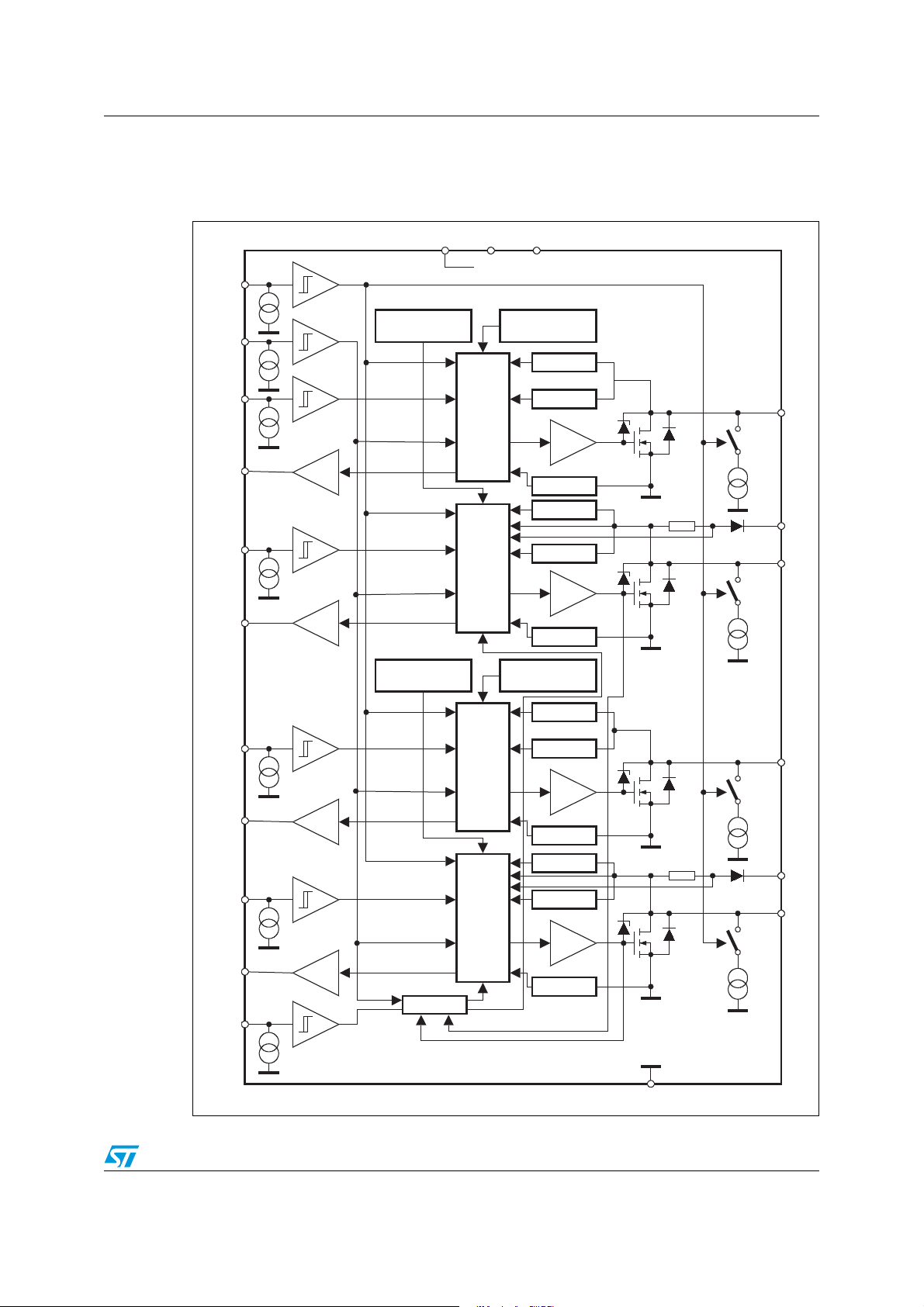
L9347 Block diagram and pin connections
99AT0059
1 Block diagram and pin connections
Figure 1. Block diagram
VS VCC VDD
Internal Supply
EN
CLK
IN1
ST1
IN4
ST4
IN2
Overtemperature
Channel 4
Overtemperature
Channel 3
LOGIC
LOGIC
&
DA
LOGIC
Overtemperature
Channel 1
Open Load
Overload
GND-det.
Open Load
Overload
GND-det.
Overtemperature
Channel 2
Open Load
Overload
Q1
IPD
D4
Q4
IPD
Q2
ST2
IN3
ST3
TEST
drift-det.
IPD
D3
Q3
IPD
LOGIC
&
DA
GND-det.
Open Load
Overload
GND-det.
GND
5/29
Page 6

Block diagram and pin connections L9347
99AT0060
Figure 2. Pin connections
CLK
PGND3
PGND3
PGND4
PGND4
Table 2. Pin description
GND 1
Q3
Q3
D3
D3
Q1
Q1
Q2
Q2
D4
D4
Q4
Q4
N.C.
2
3
4
5
6
7
8
9
10
11
12
13
14
15
16
17
18
36
35
34
33
32
31
30
29
28
27
26
25
24
23
22
21
20
19
ST3
IN1
IN3
ST1
PGND1
PGND1
VS
PGND2
PGND2
TEST
EN
ST2
IN4
IN2
ST4
VDD
VCC
N° Pin Function
1 GND Logic Ground
2, 3 PGND 3 Power Ground Channel 3
4, 5 Q 3 Power Output Channel 3
6, 7 D 3 Free-Wheeling Diode Channel 3
8, 9 Q 1 Power Output Channel 1
10, 11 Q 2 Power Output Channel 2
12, 13 D 4 Free-Wheeling Diode Channel 4
14, 15 Q 4 Power Output Channel 4
16, 17 PGND 4 Power Ground Channel 4
18 NC Not Connected
19 VCC 5V Supply
20 VDD 5V Supply
21 ST 4 Status Output Channel 4
22 IN 2 Control Input Channel 2
23 IN 4 Control Input Channel 4
24 ST 2 Status Output Channel 2
25 EN Enable Input for all four Channels
26 TEST Enable Input for Drift detection
27, 28 PGND 2 Power Ground Channel 2
29 VS Supply Voltage
6/29
Page 7

L9347 Block diagram and pin connections
Table 2. Pin description (continued)
N° Pin Function
30, 31 PGND 1 Power Ground Channel 1
32 ST 1 Status Output Channel 1
33 IN 3 Control Input Channel 3
34 IN 1 Control Input Channel 1
35 ST 3 Status Output Channel 3
36 CLK Clock Input
7/29
Page 8

Electrical specifications L9347
2 Electrical specifications
Table 3.
Electrical characteristcs
(Vs = 4.8 to 18V; T
= -40 to 150°C unless otherwise specified)
j
:
Symbol Parameter Test condition Min. Typ. Max. Unit
Power supply
V
≤ 18V
I
SON
I
SOFF
I
cc
I
dd
I
dd
Supply current
Quiescent current
Supply current VCC (analog supply) VCC =5V 5 mA
Supply current VDD (digital supply) VDD =5V f
Supply current VDD (digital supply) VDD =5V f
S
(outputs ON)
V
≤ 18V
S
(outputs OFF)
CLK
CLK
5mA
5mA
=0Hz 5 uA
=250kHz 5 mA
General diagnostic functions
VS ≥ 6.5V
(outputs OFF)
= 250 kHz 33,3 45 %
CLK
= 250 kHz 55 66,6 %
CLK
0.3 0.33 0.36 x V
DC
DC
V
V
f
CLK,min
VS
V
QU
thGND
thPGL
CLKe_low
CLKe_high
loss
Open load voltage
Signal-GND-loss threshold VCC= 5V 0.1 1 V
Power-GND-loss threshold VCC= 5V 1.5 2.5 3.5 V
Clock frequency error 10 100 kHz
Clock duty cycle error detection low f
Clock duty cycle error detection high f
Supply detection VCC = VDD = 5V 2 4.5 V
Additional diagnostic functions channel 1 and channel 2 (non regulated channels)
Q
I
QU1,2
I
QO1,2
Open-load current channel 1, 2 VS ≥ 6.5V 50 140 mA
Over-load current channel 1, 2 VS ≥ 6.5V 5 7.5 9 A
Additional diagnostic functions channel 3 and channel 4 (regulated channels)
DC
I
QO3,4
V
PWM
OUT
rerr
Output duty cycle range filtered with 10ms 10 90 %
Overload current
channel 3,4
Recirculation error shutdown
threshold (open D3/D4)
Output PWM ratio during drift
dOUT
comparison
VS ≥ 6.5V 2.5 5 8 A
Iout > 50mA 45 50 60 V
= V
V
V
IN3
TEST
IN4
= H
= PWM
IN
-14.3 +14.3 %
Digital inputs (IN1 to IN4, ENA, CLK, TEST). The valid PWM-Ratio for IN3/IN4 is 10% to 90%
V
IL
V
IH
V
IHy
Input low voltage -0.3 1 V
Input high voltage 2 6 V
Input voltage hysteresis
(1)
20 500 mV
8/29
Page 9

L9347 Electrical specifications
Table 3.
Electrical characteristcs: (continued)
(Vs = 4.8 to 18V; Tj = -40 to 150°C unless otherwise specified)
Symbol Parameter Test condition Min. Typ. Max. Unit
I
I
Digital outputs (ST1 to ST4)
V
STL
V
STH
R
DIAGL
R
DIAGH
Power outputs (Q1 to Q4)
R
DSON1,2
R
DSON3,4
Input pull down current VIN = 5V, VS ≥ 6.5V 8 20 40 μA
Status output voltage in low state
Status output voltage in high state
R
R
OUT
OUT
+ R
+ R
in low state 0.3 0.64 1.5 kΩ
DSON
in high state 1.5 3.2 7.0 kΩ
DSON
Static drain-source ON-resistance
Q1 and Q2
(non-reg. channels)
Static drain-source ON-resistance
Q3 and Q4
(reg. channels)
(2)
IST ≤ 40μA00.4V
IST ≥ -40μA 2.5 3.45 V
(2)
≥ -120μA 2 3.45 V
I
ST
= 1A; VS ≥ 9.5V
I
Q
T
= 25°C
j
= 125°C
T
j
Tj = 150°C
= 1A; VS ≥ 9.5V
I
Q
= 25°C
T
j
= 125°C
T
j
Tj = 150°C
(3)
(4)
(3)
(4)
0.2 0.5
0.5
0.35 0.75
0.75
W
W
W
Ω
Ω
Ω
V
F_250mA
V
F_2.25A
R
sens
V
I
PD
I
Qlk
Timing
t
ON
t
OFF
t
OFFREG
t
t
t
SCP
Forward voltage of free wheeling path
D3, D4 @250mA
Forward voltage of free wheeling path
D3, D4 @2.25A
Sense resistor = (V
V
F_250mA
Z-diode clamping voltage IQ ≥ 100mA 45 60 V
Z
)/2A
F_2.25A-
= -250mA 0.5 1.5 V
I
D3/4
= -2.25A 2.0 4.5 V
I
D3/4
1 Ω
Output pull down current VEN = H, VIN = L 10 150 μA
Output leakage current VEN = L; VQ = 20V 5 μA
Output ON delay time IQ = 1A 0 5 20 μs
Output OFF delay time channel IQ = 1A 0 10 30 μs
Output OFF delay time regulator
t
r
t
f
sf
lf
Output rise time IQ = 1A
Output fall time IQ = 1A
Short error detection filter time f
Long error detection filter time f
Short circuit switch-OFF delay time
(5)
= 250kHz DC = 50%
CLK
= 250kHz DC = 50%
CLK
(5)
528 μs
0.5 1.5 8 μs
0.5 1.5 8 μs
(5)
(5)
48μs
16 32 μs
430μs
9/29
Page 10

Electrical specifications L9347
Table 3.
Electrical characteristcs: (continued)
(Vs = 4.8 to 18V; Tj = -40 to 150°C unless otherwise specified)
Symbol Parameter Test condition Min. Typ. Max. Unit
(5)
(5)
(reg. channels only)
(5)
(reg. channels only
896 1024 us
10 ms
528 μs
t
t
Dreg
t
RE
D
Status delay time
Regulation error status delay time
Output off status delay time
Reg. current accuracy (reg. channels only)
I
Q3/Q4
I
Q3/Q4
I
REG
ΔI
Q3/Q4
Minimum current DC = 10% 200 250 300 mA
Maximum current DC = 90% 2 2.25 2.5 A
Max. regulation deviation @
DC 10% - 90%
250mA < I
400mA ≤ I
800mA < I
Q3/Q4
Q3/Q4
Q3/Q4
< 400mA
≤ 800mA
< 2.25A
±10
±6
±10
Min. quant. step 5 mA
Frequencies
CLK frequency crystal-controlled 250 kHz
Input PWM frequency (reg. channels only) 2 kHz
1. This parameter will not be tested but assured by design
2. Short circuit between two digital outputs (one in high the other in low state) will lead to the defined result "LOW"
3. Measured chip, bond wires not included
4. Measured on Power SO-36 devices
5. Digital filtered with external clock, only functional test
Table 4. Absolute maximum ratings
.
The absolute maximum ratings are the limiting values for this device. Damage may occur if
this device is subjected to conditions which are beyond these values
%
%
%
Symbol Parameter Test conditions Min Typ Max Unit
E
Switch off energy for inductive loads 50 mJ
Q
Volt ag es
V
V
V
V
, V
CC
V
V
, V
IN
V
CLK
V
ST
V
DRmax
Supply voltage -0.3 40 V
S
Supply voltage -0.3 6 V
DD
Output voltage static 40 V
Q
Output voltage during clamping t < 1ms 60 V
Q
Input voltage IN1 to IN4, EN II < |10|mA -1.5 6 V
EN
Input Voltage CLK -1.5 6 V
Output voltage status -0.3 6 V
Recirculation circuits D3, D4 40 V
D
max. reverse breakdown voltage of free
wheeling diodes D3, D4
55 V
10/29
Page 11

L9347 Electrical specifications
Table 4. Absolute maximum ratings (continued)
The absolute maximum ratings are the limiting values for this device. Damage may occur if
this device is subjected to conditions which are beyond these values
Symbol Parameter Test conditions Min Typ Max Unit
Currents
I
Q1/2
I
Q3/4
I
Q1/2
I
PGND1/2
I
Q3/4
I
PGND3/4
I
ST
Output current for Q1 and Q2 >5
Output current for Q3 and Q4 >3
,
Output current at reversal supply for Q1
and Q2
,
Output current at reversal supply for Q3
and Q4
-4 A
-2 A
Output current status pin -5 5 mA
internal
limited
internal
limited
A
A
ESD Protection
ESD Electrostatical Discharging MIL883C ±2kV
ESD Output Pins (Qx, Dx)
Table 5. Thermal data
vs. Common GND
(PGND1-4 + GND)
±4kV
Symbol Parameter Test conditions Min Typ Max Unit
T
T
T
stg
T
th
T
hy
R
thJC
1. This parameter will not be tested but assured by design.
Table 6. Operating range
Junction temperature T
j
Junction temperature during clamping
jc
(life time)
Storage temperature T
Overtemperature shutdown threshold
Overtemperature shutdown hysteresis
Thermal resistance junction to case R
j
Σt = 30min
Σt = 15min
stg
(1)
(1)
thJC
-40 150 °C
175
190
°C
-55 150 °C
175 200 °C
10 °C
2K/W
Symbol Parameter Test conditions Min. Typ. Max. Unit
V
, V
V
CC
dV
S
V
V
V
ST
Supply voltage 4.8 18 V
S
Supply voltage 4.5 5.5 V
DD
/dt Supply voltage transient time -1 1 V/μs
Output voltage static -0.3 40 V
Q
Output voltage induced by inductive
Q
switching
Voltage will be
limited by internal
Z-diode clamping
60 V
Output voltage status -0.3 6 V
11/29
Page 12

Electrical specifications L9347
Table 6. Operating range (continued)
Symbol Parameter Test conditions Min. Typ. Max. Unit
I
ST
T
T
Output current status -1 1 mA
Junction temperature -40 150 °C
j
Junction temperature during clamping
jc
Σ = 30min
Σ = 15min
175
190
°C
12/29
Page 13

L9347 Functional Description
3 Functional Description
3.1 Overview
The L9347 is designed to drive inductive loads (relays, electromagnetic valves) in low side
configuration. Integrated active Zener-clamp (for channel1 and 2) or free wheeling diodes
(for channel 3 and 4) allow the recirculation of the inductive loads. All four channels are
monitored with a status output. All wiring to the loads and supply pins of the device are
controlled. The device is self-protected against short circuit at the outputs and
overtemperature. For each channel one independent push-pull status output is used for a
parallel diagnostic function.
Channel 3 and 4 work as current regulator. A PWM signal on the input defines the target
output current. The output current is controlled through the output PWM of the power stage.
The regulator limits of 10% or 90% are detected and monitored with the status signal. The
current is measured during recirculation phase of the load.
A test mode compares the differences between the two regulators. This “drift” test compares
the output PWM of the regulators. By this feature a drift of the load during lifetime can be
detected.
3.2 Input circuits
The INput, CLK, TEST and ENable inputs, are active high, consist of Schmidt triggers with
hysteresis. All inputs are connected to pull-down current sources.
3.3 Output stages (not regulated) Channel 1 and 2
The two power outputs (5A) consist of DMOS power transistors with open drain output. The
output stages are protected against short circuit. Via integrated Zener clamp diodes the
overvoltage of the inductive loads due to recirculation are clamped to typ. 52V for fast shut
off of the valves. Parallel to the DMOS transistors there are internal pull-down current
sources. They are provided to assure an open load condition in the OFF state. With EN=low
this current source is switched off, but the open load comparator is still active.
3.4 Current regulator stages Channel 3 and 4
The current-regulator channels are designed to drive inductive loads. The target value of the
current is given by the duty cycle (DC) of the 2kHz PWM input signal. The following figure
shows the relation between the input PWM and the output current and the specified
accuracy
.
13/29
Page 14

Functional Description L9347
Figure 3. Input PWM to output current range
2250
n
sio
reci
p
t
n
re
r
Cu
250
800
400
OUTPUT Current [mA]
+- 6%
±10%
+-10%
10
INPUT PWM[%]
90
The ON period of the input signal is measured with a 1MHz clock, synchronized with the
external 250kHz clock. For requested precision of the output current the ratio between the
frequencies of the input signal and the external 250kHz clock has to be fixed according to
the graph shown in Figure 3.
Figure 4.
Current accuracy according to the input and clock frequency ratio
current accuracy
5.6%
112.5
125
132
0%
-10%
Regulator
switched off
f
CLK
/ f
IN
The theoretical error is zero for f
/ fIN = 125.
CLK
If the period of the input signal is longer than 132 times the period of the clock the regulator
is switched off. For a clock frequency lower than 100kHz the clock control will also disable
the regulator. For high precision applications the clock frequency and the input frequency
have to be correlated.
14/29
Page 15

L9347 Functional Description
The output current is measured during the recirculation of the load. The current sense
resistor is in series to the free wheeling diode. If this recirculation path is interrupted the
regulator stops immediately and the status output remains low for the rest of the input cycle.
The output period is 64 times the clock period. With a clock frequency of 250kHz the output
PWM frequency is 3.9kHz. The output PWM is synchronized with the first negative edge of
the input signal. After that the output and the input are asynchronous. The first period is
used to measure the current. This means the first turn-on of the power is 256μs after the first
negative edge of the input signal.
As regulator a digital PI-regulator with the Transfer function for:
KI: and KP: 0.96
0.126
---------------
z1–
for a sampling time of 256μs is realised.
To speed up the current settling time the regulator output is locked to 90% output PWM untill
the target current value is reached. This happens alsowhen the target current value
changes and the output PWM reaches 90% during the regulation. The status output gets
low if the target current value is not reached within the regulation error delay time of
t
=10ms. The output PWM is than out of the regulation range from 10% to 90%.
RE
3.5 Protective circuits
The outputs are protected against current overload, overtemperature, and power-GND-loss.
The external clock is monitored by a clock watchdog. This clock watchdog detects a minimal
frequency
f
and wrong clock duty cycles. The allowed clock duty cycle range is 45% to
CLK,min
55%. The current-regulator stages are protected against recirculation errors, when D3 or D4
is not connected. All these error conditions shut off the power stage and invert the status
output information.
3.6 Error detection
The status outputs indicate the switching state under normal conditions (status LOW = OFF;
status HIGH = ON). If an error occurs, the logic level of the status output is inverted, as listed
in the diagnostic table below. All external errors, for example open load, are filtered
internally. The following table shows the detected errors, the filter times and the detection
mode (on/off).
15/29
Page 16

Functional Description L9347
Table 7. Detected errors
ON State
EN &IN =
HIGH
OFF State
EN &IN =
LOW
Filter
time
Short circuit of the load X t
Open load
(under voltage detection)
Open load
(under current detection)
Xt
Xt
Over temperature X t
Power-GND-loss X X t
Signal-GND-loss X X t
Supply-VS-loss X X t
Clock control X X no
X
Output voltage clamp active
(regulated
no
channels)
Reset done by
EN & IN = “LOW”
sf
lf
sf
for
T
or
D
timer
timer
T
Dreg
T
D
T
D
EN & IN = “LOW”
sf
for
T
or
T
D
Dreg
in on: EN & IN = “LOW”
T
or
D
timer
timer
T
Dreg
T
D
T
D
T
D
lf
for
in off: timer
lf
lf
in on: EN & IN = “LOW”
for
T
or
T
D
Dreg
in off: timer
T
D
in on: EN & IN = “LOW”
T
or
for
in off: timer
T
D
Dreg
T
D
EN&IN=low means that at least one between enable and input is low. For the inputs IN = low
means also no input PWM. For the regulator input period longer than T
standard channel input period longer thanT
.
D
and for the
Dreg
A detected error is stored in an error register. The reset of this register is made with a timer
T
. With this approach all errors are present at the status output at least for the time TD.
D
All protection functions like short circuit of the output, overtemperature, clock failure or
power-GND-loss in ON condition are stored into an internal “fail” register. The output is then
shut off. The register must be reset with a low signal at the input. A “low signal” means that
the input is low for a time longer than T
D
or T
for the reulated channel, otherwise it is
DReg
interpreted as a PWM input signal and the register is left in set mode.
Signal-GND-loss and VS-loss are detected in the active on mode, but they do not set the fail
register. This type of error is only delayed with the standard timer
t
function.
lf
Open load is detected for all four channels in on and off state.
Open load in off condition detects the voltage on the output pin. If this voltage is below 0.33
* VS the error register is set and delayed with T
. A sink current stage pull the output down
D
to ground, with EN high. With EN low the output is floating in case of openload and the
detection is not assured. In the ON state the load current is monitored by the non-regulated
channels. If it drops below the specified threshold value I
the error register is set and delayed with T
. A regulated channel detects the open load in
D
an open load is detected and
QU
the on state with the current regulator error detection. If the output PWM reaches 90% for a
time longer than t
than an error occurs. This could happen when no load is connected, the
RE
16/29
Page 17

L9347 Functional Description
resistivity of the load is too high or the supply voltage too low. The same error is shown if the
regulator is not able to reduce the current in the load in the time t
, so the output PWM falls
RE
below 10%.
A clock failure (clock loss) is detected when the frequency becomes lower than
status outputs are set on error and all power outputs are shut off. The status signals remain
in their state until the clock signal is present again. A clock failure during power on of VCC is
detected only on the regulated channels. The status outputs of the channel 1 and 2 are low
in this case.
3.7 Drift detection (regulated channels only)
The drift detection is used to compare the two regulated channels during regulation. This
“Drift” test compares the output PWM of the regulators. The resistivity of the load influences
the output PWM. The approximated formula for the output current below shows the
dependency of the load resistor to the output PWM. In this formula the energy reduction
during the recirculation is not taken into account. The real output PWM is higher. The
testmode is enabled with IN,EN and TEST high. With an identical 2kHz PWM-Signal
connected to the IN-inputs the output PWM must be in a range of +-14.3%. If the difference
between the two on-times is more than ±14.3% of the expected value an error is detected
and monitored by the status outputs, in the same way as described above, but a drift error
will not be registered and also not delayed with T
VBAT
IOUT
----------------------------
RL RON+
Drift Definition:
as other errors
D
PWM⋅=
f
CLK,min
. All
E.. not correlated Error of the channels
%PWM ... Corresponding ideal output PWM to a given input PWM
A 7bit output-PWM-register is used for the comparison. The register with the lower value is
subtracted from the higher one. This result is multiplied by four and compared with the
higher value.
3.8 Other test modes
The test pin is also used to test the regulated channels in the production. With a special
sequence on this pin the power stages of the regulated channels can be controlled direct
from the input. No status feedback of the regulated channels is given. The status output is
clocked by the regulator logic. The output sequence is a indication of a proper logic
functionality. The functionality of this special test mode is shown in Ta ble 8.
Drift = PWM(1+E) - PWM (1-E) = 2PWM E
Drift * 4 < PWM (1+E)
with E >14.3% a drift is detected
17/29
Page 18

Functional Description L9347
Table 8. Special test mode functionality
EN In Test Out Status Note
1 X X X X disable test mode
1 1 1 on 1 Drift mode
0 X off test pattern test condition one
0 X off test pattern test condition two
0 X off test pattern test condition three
0 0 off test pattern test condition four
0 1 on test pattern test condition four
For more details about the test conditions see timing diagrams in Section 4.
3.9 Diagnostic table
The status follows the input signal in normal operating conditions.
If any error is detected the status is inverted.
Table 9. Diagnostic table
Operating Condition
Normal function
Open load or short to ground
Overload or short to supply
Latched overload
Reset latch
Reset latch
Overtemperature
Latched overtemperature
Reset latch
Reset latch
Recirculation error (reg.chn.)
Latched error
Reset latch
Reset latch
Test
Input
TEST
L
L
L
L
L
L
L
L
L
L
L
L
L
L
L
L
L
L
L
L
Enable
Input
ENA
L
L
H
H
L
L
H
H
H
H
H –> L
H
H
H
H –> L
H
H
H
H –> L
H
Control
Input non-
reg./reg. IN
L
H/PWM
L
H/PWM
L
H/PWM
L
H/PWM
H/PWM
H/PWM
X
H/PWM –> L
H/PWM
H/PWM
X
H/PWM –> L
PWM
PWM
X
PWM –> L
Power
Output/
ent reg. Q
OFF
OFF
OFF
ON
OFF
OFF
OFF
ON
OFF
OFF
OFF
OFF
OFF
OFF
OFF
OFF
OFF
OFF
OFF
OFF
Curr
Status
Output
ST
L
L
L
H
X
X
H
L
L
L
L
L
L
L
L
L
L
L
L
L
18/29
Page 19

L9347 Functional Description
Table 9. Diagnostic table (continued)
Test
Operating Condition
Input
TEST
L
Clock failure (clock loss)
(1)
L
L
L
Drift
(2)
H
H
Failure
No failure
1. During power on sequence only detected on channel 3 and 4 (see description).
2. This input combination is also used for an internal chip-test and must not be used.
H
H
Enable
Input
ENA
L
L
H
H
L
L
H
H
Control
Input non-
reg./reg. IN
L
H/PWM
L
H/PWM
L
H/PWM
H/PWM
H/PWM
Output/
Power
Curr
ent reg. Q
OFF
OFF
OFF
OFF
OFF
OFF
ON
ON
Status
Output
ST
H
H
H
L
X
X
L
H
19/29
Page 20
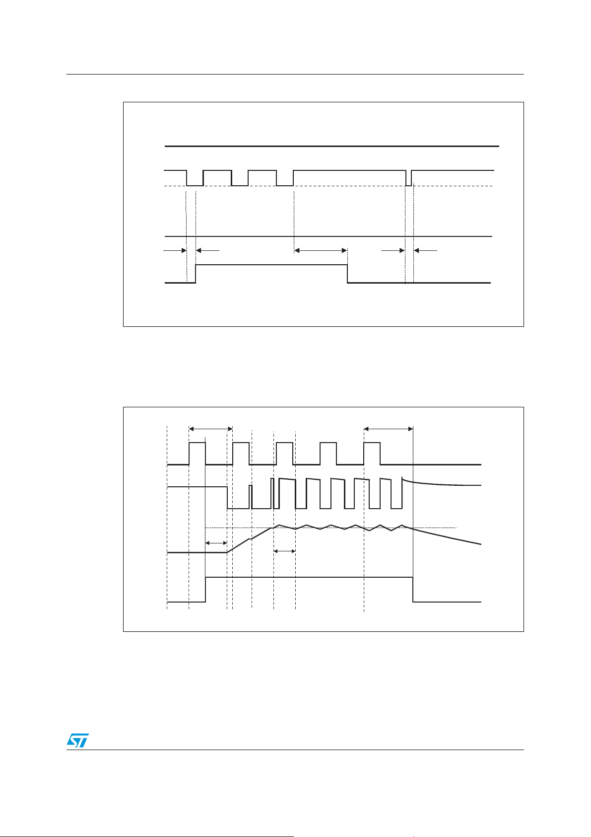
Timing diagrams L9347
9
00RS0001
4 Timing diagrams
4.1 Non regulated channels
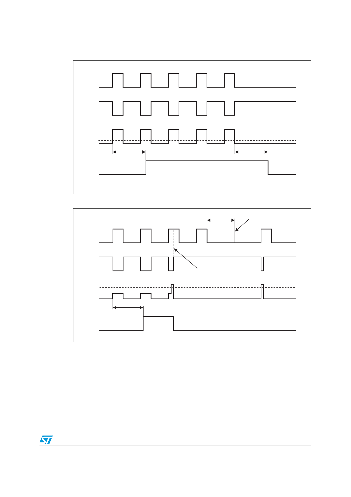
Figure 5. Output slope, resistive load
V
I
V
IH
V
IL
t
t
OFFtr
85% V
15% V
t
V
Q
V
S
S
S
ONtf
9AT0061
Figure 6. Overload switch OFF delay
I
Q
I
QO
I
QU
t
D
V
ST
t
t
SCP
t
sf
t
t
20/29
Page 21
L9347 Timing diagrams
9
99AT0064
Figure 7. Normal condition, resistive load, pulsed input signal
V
IN
V
Q
I
Q
t
D
V
ST
9AT0063
Figure 8. Current overload
V
IN
V
Q
I
Q
t
D
Set Fail
register
I
QU
t
D
t
D
Reset Fail
register
I
QO
V
ST
21/29
Page 22
Timing diagrams L9347
9
9
Figure 9 and Figure 10 show diagnostic status output at different OPEN load current
conditions followed by normal operation.
Figure 9. Under current condition
t
D
V
IN
V
Q
I
Q
t
D
V
ST
9AT0065
Figure 10. Open load condition in the case of pulsed input signal
V
IN
V
Q
I
Q
t
D
I
QU
t
D
I
QU
V
ST
9AT0066
22/29
Page 23
L9347 Timing diagrams
9
9
Figure 11. Pulsed open load conditions (regulated and non-regulated channels)
V
IN
V
Q
I
Q
V
ST
9AT0067
t
lf
t
D
0.33 x V
S
t
lf
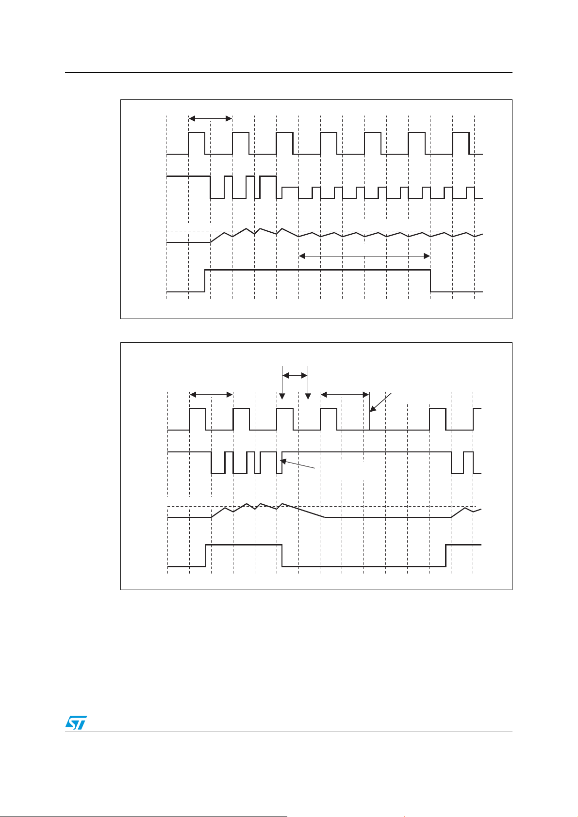
4.2 Regulated channels (timing diagrams of diagnostic with 2kHz PWM input signal)
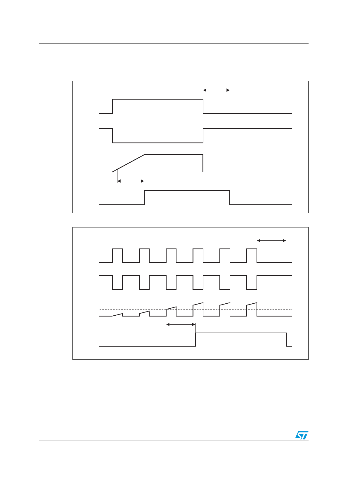
Figure 12. Normal condition, inductive load
500μs
V
IN
t
DREG
V
Q
I
Q
V
ST
9AT0068
Target Current
256μs
256μs
23/29
Page 24
Timing diagrams L9347
9
99AT0070
Figure 13. Current overload
500μs
V
IN
V
Q
I
QO
I
Q
V
ST
9AT0069
Figure 14. Recirculation error
500μs
V
IN
t
DREG
Reset Fail
register
Set fail
registor
t
sf
t
DREG
Reset Fail
register
V
Q
I
Q
V
ST
Set Fail
register
target current
24/29
Page 25
L9347 Timing diagrams
9
Figure 15. Current regulation error (e.g. as a result of voltage reduction)
500μs
V
IN
V
Q
PWM
= 90%
I
Q
V
ST
9AT0071
target current
ratio
t
RE
Figure 16. Over temperature
Over temperature
Condition
V
IN
V
Q
I
Q
V
ST
99AT0072
500ms
target current
t
DREG
Set Fail
register
Reset Fail
register
25/29
Page 26

Timing diagrams L9347
Figure 17. Test mode 4 VEN low
V
TEST
V
IN3/4
V
Q3/4
99AT0073
26/29
Page 27

L9347 Package information
5 Package information
In order to meet environmental requirements, ST offers these devices in ECOPACK®
packages. These packages have a lead-free second level interconnect. The category of
second level interconnect is marked on the package and on the inner box label, in
compliance with JEDEC standard JESD97. The maximum ratings related to soldering
conditions are also marked on the inner box label. ECOPACK is an ST trademark.
ECOPACK specifications are available at: www.st.com.
Figure 18. PowerSO-36 mechanical data and package dimensions
DIM.
A 3.60 0.1417
a1 0.10 0.30 0.0039 0.0118
a2 3.30 0.1299
a3 0 0.10 0.0039
b 0.22 0.38 0.0087 0.0150
c 0.23 0.32 0.0091 0.0126
D 15.80 16.00 0.6220 0.6299
D1 9.40 9.80 0.3701 0.3858
E 13.90 14.5 0.5472 0.5709
E1 10.90 11.10 0.4291 0.4370
E2 2.90 0.1142
E3 5.80 6.20 0.2283 0.2441
e 0.65 0.0256
e3 11.05 0.4350
G 0 0.10 0.0039
H 15.50 15.90 0.6102 0.6260
h 1.10 0.0433
L 0.8 1.10 0.0315 0.0433
N 10˚ (max)
s 8˚ (ma x)
Note: “D and E1” do not include mold flash or protusions.
- Mold flash or protusions shall not exceed 0.15mm (0.006”)
- Critical dimensions are "a3", "E" and "G".
mm inch
MIN. TYP. MAX. MIN. TYP. MAX.
OUTLINE AND
MECHANICAL DATA
PowerSO-36
0096119 C
27/29
Page 28

Revision history L9347
6 Revision history
Table 10. Document revision history
Date Revision Changes
06-July-2002 1 Initial release.
02-May-2007 2 Package change, text modifications, corporate layout changes.
28/29
Page 29

L9347
Please Read Carefully:
Information in this document is provided solely in connection with ST products. STMicroelectronics NV and its subsidiaries (“ST”) reserve the
right to make changes, corrections, modifications or improvements, to this document, and the products and services described herein at any
time, without notice.
All ST products are sold pursuant to ST’s terms and conditions of sale.
Purchasers are solely responsible for the choice, selection and use of the ST products and services described herein, and ST assumes no
liability whatsoever relating to the choice, selection or use of the ST products and services described herein.
No license, express or implied, by estoppel or otherwise, to any intellectual property rights is granted under this document. If any part of this
document refers to any third party products or services it shall not be deemed a license grant by ST for the use of such third party products
or services, or any intellectual property contained therein or considered as a warranty covering the use in any manner whatsoever of such
third party products or services or any intellectual property contained therein.
UNLESS OTHERWISE SET FORTH IN ST’S TERMS AND CONDITIONS OF SALE ST DISCLAIMS ANY EXPRESS OR IMPLIED
WARRANTY WITH RESPECT TO THE USE AND/OR SALE OF ST PRODUCTS INCLUDING WITHOUT LIMITATION IMPLIED
WARRANTIES OF MERCHANTABILITY, FITNESS FOR A PARTICULAR PURPOSE (AND THEIR EQUIVALENTS UNDER THE LAWS
OF ANY JURISDICTION), OR INFRINGEMENT OF ANY PATENT, COPYRIGHT OR OTHER INTELLECTUAL PROPERTY RIGHT.
UNLESS EXPRESSLY APPROVED IN WRITING BY AN AUTHORIZED ST REPRESENTATIVE, ST PRODUCTS ARE NOT
RECOMMENDED, AUTHORIZED OR WARRANTED FOR USE IN MILITARY, AIR CRAFT, SPACE, LIFE SAVING, OR LIFE SUSTAINING
APPLICATIONS, NOR IN PRODUCTS OR SYSTEMS WHERE FAILURE OR MALFUNCTION MAY RESULT IN PERSONAL INJURY,
DEATH, OR SEVERE PROPERTY OR ENVIRONMENTAL DAMAGE. ST PRODUCTS WHICH ARE NOT SPECIFIED AS "AUTOMOTIVE
GRADE" MAY ONLY BE USED IN AUTOMOTIVE APPLICATIONS AT USER’S OWN RISK.
Resale of ST products with provisions different from the statements and/or technical features set forth in this document shall immediately void
any warranty granted by ST for the ST product or service described herein and shall not create or extend in any manner whatsoever, any
liability of ST.
ST and the ST logo are trademarks or registered trademarks of ST in various countries.
Information in this document supersedes and replaces all information previously supplied.
The ST logo is a registered trademark of STMicroelectronics. All other names are the property of their respective owners.
© 2007 STMicroelectronics - All rights reserved
STMicroelectronics group of companies
Australia - Belgium - Brazil - Canada - China - Czech Republic - Finland - France - Germany - Hong Kong - India - Israel - Italy - Japan -
Malaysia - Malta - Morocco - Singapore - Spain - Sweden - Switzerland - United Kingdom - United States of America
www.st.com
29/29
 Loading...