

Features
■ Wide operating supply voltage range from
4.5 V up to 32 V for transient 45 V
■ Very low stand-by quiescent current < 2 µA
■ Input to output signal transfer function
programmable
■ High signal range from -0.3 V up to 32 V for all
inputs
■ TTL and CMOS compatible inputs
■ Defined output off state for open inputs
■ Four open drain DMOS outputs, with
R
= 1.5 Ω for VS > 6 V at 25 °C
DSon
■ Output current limitation
■
Controlled output slope for low EMI
■ Over temperature protection for each channel
■ Integrated output clamping for fast inductive
recirculation V
■ Status monitoring for
> 45 V
FB
– Over temperature
– Disconnected ground or supply voltage
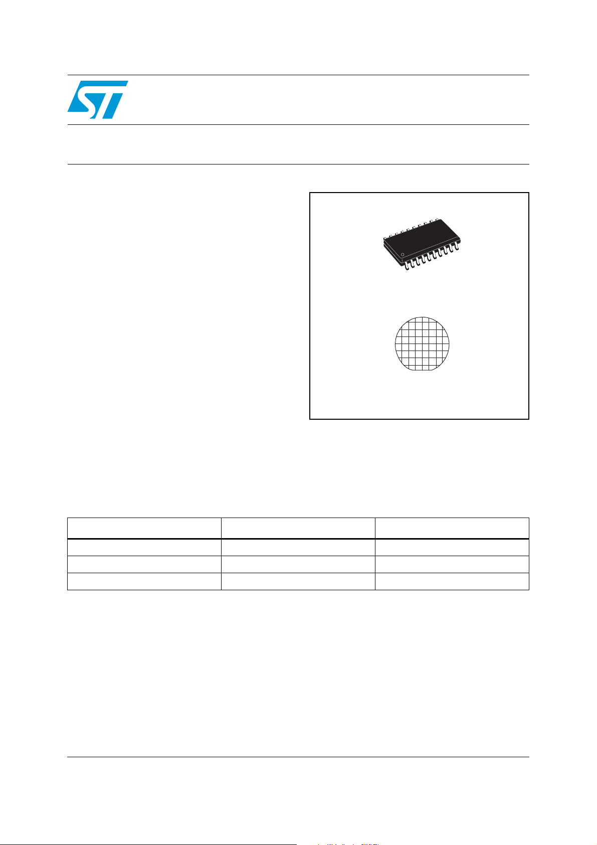
Table 1. Device summary
L9339
Quad low side driver
SO20
BARE DIE
Description
The L9339 is a monolithic integrated quad low
side driver. It is intended to drive lines, lamps or
relays in automotive or industrial applications.
Order code Package Packing
L9339 SO20 Tube
L9339DIE1 DIE Bare die
L9339MD
1. Obsolete order code.
June 2008 Rev 2 1/14
(1)
SO20 Tube
www.st.com
1

Contents L9339
Contents
1 Block diagram . . . . . . . . . . . . . . . . . . . . . . . . . . . . . . . . . . . . . . . . . . . . . . 5
2 Pins description . . . . . . . . . . . . . . . . . . . . . . . . . . . . . . . . . . . . . . . . . . . . 6
3 Electrical specifications . . . . . . . . . . . . . . . . . . . . . . . . . . . . . . . . . . . . . . 7
3.1 Absolute maximum ratings . . . . . . . . . . . . . . . . . . . . . . . . . . . . . . . . . . . . . 7
3.2 Thermal data . . . . . . . . . . . . . . . . . . . . . . . . . . . . . . . . . . . . . . . . . . . . . . . 7
3.3 Electrical characteristics . . . . . . . . . . . . . . . . . . . . . . . . . . . . . . . . . . . . . . . 8
4 Functional description . . . . . . . . . . . . . . . . . . . . . . . . . . . . . . . . . . . . . . 10
5 Package information . . . . . . . . . . . . . . . . . . . . . . . . . . . . . . . . . . . . . . . . 12
6 Revision history . . . . . . . . . . . . . . . . . . . . . . . . . . . . . . . . . . . . . . . . . . . 13
2/14

L9339 List of figures
List of figures
Figure 1. Block diagram . . . . . . . . . . . . . . . . . . . . . . . . . . . . . . . . . . . . . . . . . . . . . . . . . . . . . . . . . . . . 5
Figure 2. Pins connection (top view) . . . . . . . . . . . . . . . . . . . . . . . . . . . . . . . . . . . . . . . . . . . . . . . . . . 6
Figure 3. Timing characteristics . . . . . . . . . . . . . . . . . . . . . . . . . . . . . . . . . . . . . . . . . . . . . . . . . . . . . . 9
Figure 4. Application for inverting transfer polarity. . . . . . . . . . . . . . . . . . . . . . . . . . . . . . . . . . . . . . . 11
Figure 5. Application for non inverting transfer polarity . . . . . . . . . . . . . . . . . . . . . . . . . . . . . . . . . . . 11
Figure 6. SO20 mechanical data and package dimensions. . . . . . . . . . . . . . . . . . . . . . . . . . . . . . . . 12
3/14

List of tables L9339
List of tables
Table 1. Device summary . . . . . . . . . . . . . . . . . . . . . . . . . . . . . . . . . . . . . . . . . . . . . . . . . . . . . . . . . . 1
Table 2. Pins function . . . . . . . . . . . . . . . . . . . . . . . . . . . . . . . . . . . . . . . . . . . . . . . . . . . . . . . . . . . . . 6
Table 3. Absolute maximum ratings . . . . . . . . . . . . . . . . . . . . . . . . . . . . . . . . . . . . . . . . . . . . . . . . . . 7
Table 4. Thermal data. . . . . . . . . . . . . . . . . . . . . . . . . . . . . . . . . . . . . . . . . . . . . . . . . . . . . . . . . . . . . 7
Table 5. Electrical characteristics . . . . . . . . . . . . . . . . . . . . . . . . . . . . . . . . . . . . . . . . . . . . . . . . . . . . 8
Table 6. Diagnostic . . . . . . . . . . . . . . . . . . . . . . . . . . . . . . . . . . . . . . . . . . . . . . . . . . . . . . . . . . . . . . 10
Table 7. Document revision history . . . . . . . . . . . . . . . . . . . . . . . . . . . . . . . . . . . . . . . . . . . . . . . . . 13
4/14
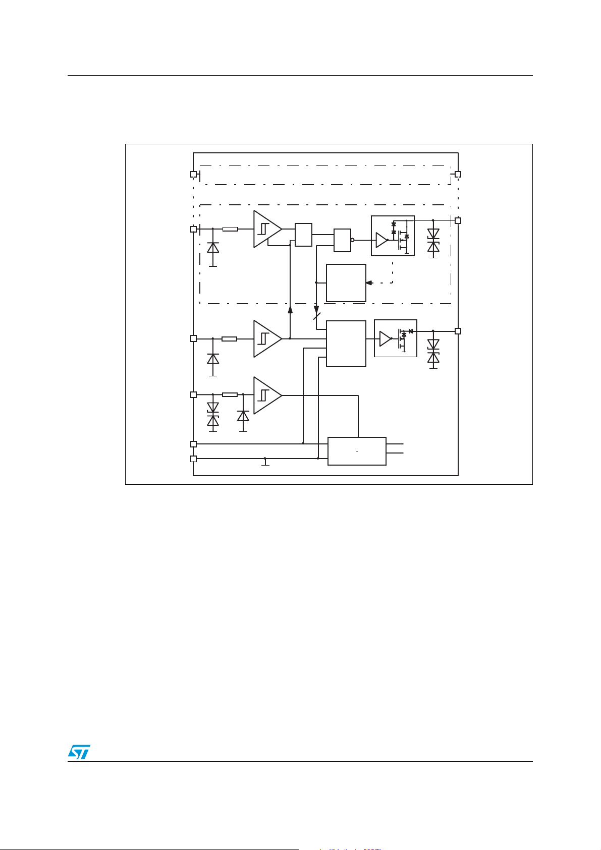
L9339 Block diagram
1 Block diagram
Figure 1. Block diagram
IN 4
IN 1
PRG
EN
VS
GND
CHANNEL4
CHANNEL1
OUT 4
OUT 1
=
&
THERMAL
SHUTDOWN
4
DIAGNOSTIC
LOGIC
REFERENCE
DIAG
Vint
Vlogic
5/14

Pins description L9339
2 Pins description
Figure 2. Pins connection (top view)
Table 2. Pins function
NC
VS
NC
IN3
IN4
EN
OUT4
OUT3
GND NC
NC NC
2
3
4
5
6
7
8
9
10
SO20
20
19
18
17
16
15
14
13
12
11
Pins # Pin Name Description
2 VS Supply Voltage
9 GND Ground
6 EN Enable
15 PRG Programing
19 DIAG Diagnostic
NC1
DIAG
NC
IN2
IN1
PRG
OUT1
OUT2
16 IN 1 Input 1
17 IN 2 Input 2
4 IN 3 Input 3
5 IN 4 Input 4
14 OUT 1 OUTPUT 1
13 OUT 2 OUTPUT 2
8 OUT 3 OUTPUT 3
7OUT4OUTPUT4
1,3,10,11,12,18,20 NC Not Connected
6/14

L9339 Electrical specifications
3 Electrical specifications
3.1 Absolute maximum ratings
Table 3. Absolute maximum ratings
Symbol Parameter Value Unit
V
dV
, V
V
IN
I
V
V
OUT
I
OUT
V
DIAG
1. In flyback phase the output voltage can reach 60 V.
ESD according to MIL 883C; tested at 2 kV; corresponds to maximum energy dissipation 0.2 mJ.
Supply voltage DC
S
/dt Supply voltage transient -10 to +10 V/µs
S
Input, Programming DC voltage
PRG
Input, Programming Pulse (T <
Negative input current -10 mA
IN
Enable voltage DC
EN
Enable voltage Pulse (T <
Output voltage -0.3 to 45
Negative output current
Positive output current
Diagnostic output voltage DC
Diagnostic output voltage Pulse (T <
3.2 Thermal data
Table 4. Thermal data
Symbol Parameter Min. Typ. Max. Unit.
Pulse (T < 400 ms)
400 ms)
400ms)
400ms)
-0.3 to 32
-0.3 to 45
-0.3 to 32
-0.3 to 45
-24 to 32
-24 to 45
(1)
-1
internal limited
-0.3 to 32
-0.3 to 45
V
V
V
V
A
V
T
JSDon
T
JSDoff
R
th j-amb
1. Mounted on SMPCB2 board
Temperature shutdown switch-on-threshold 160 200 °C
Temperature shutdown switch-off-threshold 140 180 °C
Thermal resistance junction to ambient
(1))
97 °C/W
7/14

Electrical specifications L9339
3.3 Electrical characteristics
The electrical characteristics are valid within the below defined operating conditions, unless
otherwise specified. The function is guaranteed by design until T
V
= 4.5 to 32 V; Tj = -40 to 150 °C; T
S
-40 to 125 °C; Ambient test temperature = -40 to
amb =
125 °C.
Table 5. Electrical characteristics
Symbol Parameter Test condition Min. Typ. Max. Unit
Supply
switch-on-threshold.
JSDon
I
Quiescent current
Q
Inputs, IN1 - IN4; Programming, PRG
V
V
INhigh
INlow
Input voltage low -0.3 2.0 V
Input voltage high 2.8 32 V
Input current VIN = 0 to 32V -15 25 µA
I
IN
Enable EN
V
ENlow
V
ENhigh
R
I
Input voltage low -24 1 V
Input voltage high 3.2 V
Input impedance -24 V < VIN < 2.5 V 10 kΩ
EN
Input current 2.5 V < VIN < 32 V 20 80 µA
EN
Outputs OUT1- OUT4
R
DSon
I
OLeak
V
OClamp
Output ON-resistor VS > 6 V, IO = 0.3 A 1.7 3.8 Ω
Leakage current
Output voltage during clamping
-0.3 V <
Ta < 125 °C
-0.3 V <
Ta < 150 °C
V
V
V
time < 200 µs
10 mA <
VEN < 0.5 V; VS = 14 V;
VEN < 0.5 V; VS = 14 V;
> 3.2 V; VS < 14 V 1.5 2 mA
EN
= 14 V; Ta < 125 °C <15µA
O =VS
= 14 V; Ta < 150 °C 25 µA
O=VS
IO < 0.3 A
45 52 60 V
< 2 10 µA
50 µA
S
V
I
OSC
C
Short-circuit current
> 6 V 0.4 0.7 1 A
V
S
internal output capacities VO > 4.5 V 100 pF
O
Diagnostic output DIAG
4.5V < VS < 6 V 0.3 1 A
V
I
Dmax
Output voltage LOW I
Dlow
Maximum output current
< 0.6 mA 1.3 V
DL
internal current limitation
= 14 V
V
D
8/14
1515mA

L9339 Electrical specifications
Table 5. Electrical characteristics (continued)
Symbol Parameter Test condition Min. Typ. Max. Unit
V
= VS = 14 V; Ta < 125 °C < 0.1 1 µA
I
DLeak
Leakage current
Timing characteristics
(1)
D
V
= VS = 14 V; Ta < 150 °C 5 µA
D
t
d,on
t
d,off
t
t
d,DIAG
S
On delay time
Off delay time 3 4.5 µs
Enable settling time 10 µs
set
V
10 mA <
ON or OFF diagnostic delay time 10 µs
Output voltage slopes
out
(2)
1. See also Figure 3 timing characteristics.
2. Output voltage slope not controlled for enable low.
All parameters are measured at T
= 125 °C.
amb
Figure 3. Timing characteristics
V
EN
V
INhigh
V
IN lo w
V
PRG
V
V
INhigh
IN lo w
Non-Inverting Mode Inverting Mode
= 14 V, C
S
= 0 pF
ext
IO < 200 mA
active
23.5µs
2.5 9 16 V/µs
t
V
V
V
1/2 V
V
INhigh
IN lo w
OUT
V
t
IN
t
S
S
t
set
t
d,offtd,on
t
d,offtd,on
t
d,offtd,on
5)
t
t
set
9/14

Functional description L9339
4 Functional description
The L9339 is a quad low side driver for lines, lamps or inductive loads in automotive and
industrial applications.
The logic input levels are TTL and CMOS compatible. This allows the device to be driven
directly by a microcontroller. For the noise immunity, all input thresholds has a hysteresis of
typ. 100 mV. At each input (IN and PRG) voltages from -0.3 V to 32 V can be applied, EN
can withstand voltages from -25 V to 3 2 V. The device is activated with a 'high' signal on
ENable. ENable 'low' switches the device into the sleep mode. In this mode the quiescent
current is less than 10 µA. A high signal on PRoGramming input changes the signal transfer
polarity from non inverting into the inverting mode. This pin can be connected to V
The forced status of the PRG and EN pin is low, if these pins are not connected. This forced
condition leads to a mode change if the PRG pin was high before the interruption.
Independent of the PRoGramming input, the OUTput switches off, if the signal INput pin is
not connected.
Each output driver has a current limitation of min 0.4 A and a independent thermal shutdown. The thermal shut-down deactivates that output, which exceeds temperature switch off
level. When the junction temperature decreases 20 K below this temperature threshold the
output will be activated again (hysteresis of the thermal shutdown function). The slew rate
of the output voltage is limited to max. 14 V/µs, to reduce the electromagnetic radiation of
the loads and its wiring. For inductive loads a output voltage clamp of typically 52 V is
implemented.
or GND.
S
The DIAGnostic is an open drain output with an additional series diode. The logic status
depends on the PRoGramming pin. If the PRG pin is 'low' the DIAG output becomes low, if
the device works correctly. At thermal shut-down of one channel the DIAGnostic output
becomes high. If the PRG pin is 'high' this output is switched off at normal function and
switched on at over temperature.
Table 6. Diagnostic
Pins EN PRG IN OUT DIAG
H L L L (on) L (on)
H L H H (off) L (on)
Correct function
Over temperature or
supply voltage
Over temperature H H X H (off)
1. Selective for each channel at over temperature
X = not relevant
H = high
L = low
H H L H (off) H (off)
H H H L (on) H (off)
L X X H (off) H (off)
H L X H (off)
(1)
(1)
H (off)
L (on)
10/14

L9339 Functional description
Figure 4. Application for inverting transfer polarity
BOARD VOLTAGE 14 V
VCC = 5V
10µF
VCC
MICROCONTROLLER
GND
INT
D 0
D 1
D 2
D 3
AdressdecoderA 0:8
8
PRG
EN
IN 1
IN 2
IN 3
IN 4
VS
L9339
OUT 1
OUT 2
OUT 3
OUT 4
GND
DIAG
2 W 12 mH
50 kHz
Figure 5. Application for non inverting transfer polarity
BOARD VOLTAGE 14 V
10µF
VS
PRG
L9339
GND
DIAG
2 W 12 mH
OUT 1
OUT 2
OUT 3
OUT 4
EN
IN 1
IN 2
IN 3
IN 4
10µH
10µH
M
250 mA
240
50pF
M
250 mA
240
50pF
VCC = 5V
VCC
IN
GND
VCC = 5V
VCC
IN
GND
1. We recommend to use the device for driving inductive loads with flyback energy EFB < 2mJ.
11/14

Package information L9339
5 Package information
In order to meet environmental requirements, ST (also) offers these devices in ECOPACK®
packages. ECOPACK
®
packages are lead-free. The category of second Level Interconnect
is marked on the package and on the inner box label, in compliance with JEDEC Standard
JESD97. The maximum ratings related to soldering conditions are also marked on the inner
box label.
ECOPACK is an ST trademark. ECOPACK specifications are available at: www.st.com.
Figure 6. SO20 mechanical data and package dimensions
DIM.
A 2.35 2.65 0.093 0.104
A1 0.10 0.30 0.004 0.012
B 0.33 0.51 0.013 0.200
C 0.23 0.32 0.009 0.013
(1)
D
E 7.40 7.60 0.291 0.299
e 1.27 0.050
H 10.0 10.65 0.394 0.419
h 0.25 0.75 0.010 0.030
L 0.40 1.27 0.016 0.050
k 0˚ (min.), 8˚ (max.)
ddd 0.10 0.004
(1) “D” dimensio n does not include mold flash, prot usions or gate
burrs. Mol d flash, prot usions or gat e burrs shal l not exceed
0.15mm per sid e.
mm inch
MIN. TYP. MAX. MIN. TYP. MAX.
12.60 13.00 0.496 0.512
OUTLINE AND
MECHANICAL DATA
SO20
12/14
0016022 D

L9339 Revision history
6 Revision history
Table 7. Document revision history
Date Revision Changes
20-Dec-1999 1 Initial release.
Document reformatted.
24-Jun-2008 2
Updated the Table 1: Device summary.
Updated the Figure 5.
13/14

L9339
Please Read Carefully:
Information in this document is provided solely in connection with ST products. STMicroelectronics NV and its subsidiaries (“ST”) reserve the
right to make changes, corrections, modifications or improvements, to this document, and the products and services described herein at any
time, without notice.
All ST products are sold pursuant to ST’s terms and conditions of sale.
Purchasers are solely responsible for the choice, selection and use of the ST products and services described herein, and ST assumes no
liability whatsoever relating to the choice, selection or use of the ST products and services described herein.
No license, express or implied, by estoppel or otherwise, to any intellectual property rights is granted under this document. If any part of this
document refers to any third party products or services it shall not be deemed a license grant by ST for the use of such third party products
or services, or any intellectual property contained therein or considered as a warranty covering the use in any manner whatsoever of such
third party products or services or any intellectual property contained therein.
UNLESS OTHERWISE SET FORTH IN ST’S TERMS AND CONDITIONS OF SALE ST DISCLAIMS ANY EXPRESS OR IMPLIED
WARRANTY WITH RESPECT TO THE USE AND/OR SALE OF ST PRODUCTS INCLUDING WITHOUT LIMITATION IMPLIED
WARRANTIES OF MERCHANTABILITY, FITNESS FOR A PARTICULAR PURPOSE (AND THEIR EQUIVALENTS UNDER THE LAWS
OF ANY JURISDICTION), OR INFRINGEMENT OF ANY PATENT, COPYRIGHT OR OTHER INTELLECTUAL PROPERTY RIGHT.
UNLESS EXPRESSLY APPROVED IN WRITING BY AN AUTHORIZED ST REPRESENTATIVE, ST PRODUCTS ARE NOT
RECOMMENDED, AUTHORIZED OR WARRANTED FOR USE IN MILITARY, AIR CRAFT, SPACE, LIFE SAVING, OR LIFE SUSTAINING
APPLICATIONS, NOR IN PRODUCTS OR SYSTEMS WHERE FAILURE OR MALFUNCTION MAY RESULT IN PERSONAL INJURY,
DEATH, OR SEVERE PROPERTY OR ENVIRONMENTAL DAMAGE. ST PRODUCTS WHICH ARE NOT SPECIFIED AS "AUTOMOTIVE
GRADE" MAY ONLY BE USED IN AUTOMOTIVE APPLICATIONS AT USER’S OWN RISK.
Resale of ST products with provisions different from the statements and/or technical features set forth in this document shall immediately void
any warranty granted by ST for the ST product or service described herein and shall not create or extend in any manner whatsoever, any
liability of ST.
ST and the ST logo are trademarks or registered trademarks of ST in various countries.
Information in this document supersedes and replaces all information previously supplied.
The ST logo is a registered trademark of STMicroelectronics. All other names are the property of their respective owners.
© 2008 STMicroelectronics - All rights reserved
STMicroelectronics group of companies
Australia - Belgium - Brazil - Canada - China - Czech Republic - Finland - France - Germany - Hong Kong - India - Israel - Italy - Japan -
Malaysia - Malta - Morocco - Singapore - Spain - Sweden - Switzerland - United Kingdom - United States of America
www.st.com
14/14
 Loading...