

L6997S
STEP DOWN CONTROLLER
FOR LOW VOLTAGE OPERATIONS
1 Features
■ FROM 3V TO 5.5V V
■ MINIMUM OUTPUT VOLTAGE AS LOW AS
0.6V
■ 1V TO 35V INPUT VOLTAGE RANGE
■ CONSTANT ON TIME TOPOLOGY
■ VERY FAST LOAD TRANSIENTS
■ 0.6V, ±1% VREF
■ SELECTABLE SINKING MODE
■ LOSSLESS CURRENT LIMIT, AVAILABLE
ALSO IN SINKING MODE
■ REMOTE SENSING
■ OVP,UVP LATCHED PROTECTIONS
■ 600µA TYP QUIESCENT CURRENT
■ POWER GOOD AND OVP SIGNALS
■ PULSE SKIPPING AT LIGTH LOADS
■ 94% EFFICIENCY FROM 3.3V TO 2.5V
RANGE
CC
2 Applications
■ NETWORKING
■ DC/DC MODULES
■ DISTRIBUTED POWER
■ MOBILE APPLICATIONS
■ CHIP SET, CPU, DSP AND MEMORIES
SUPPLY
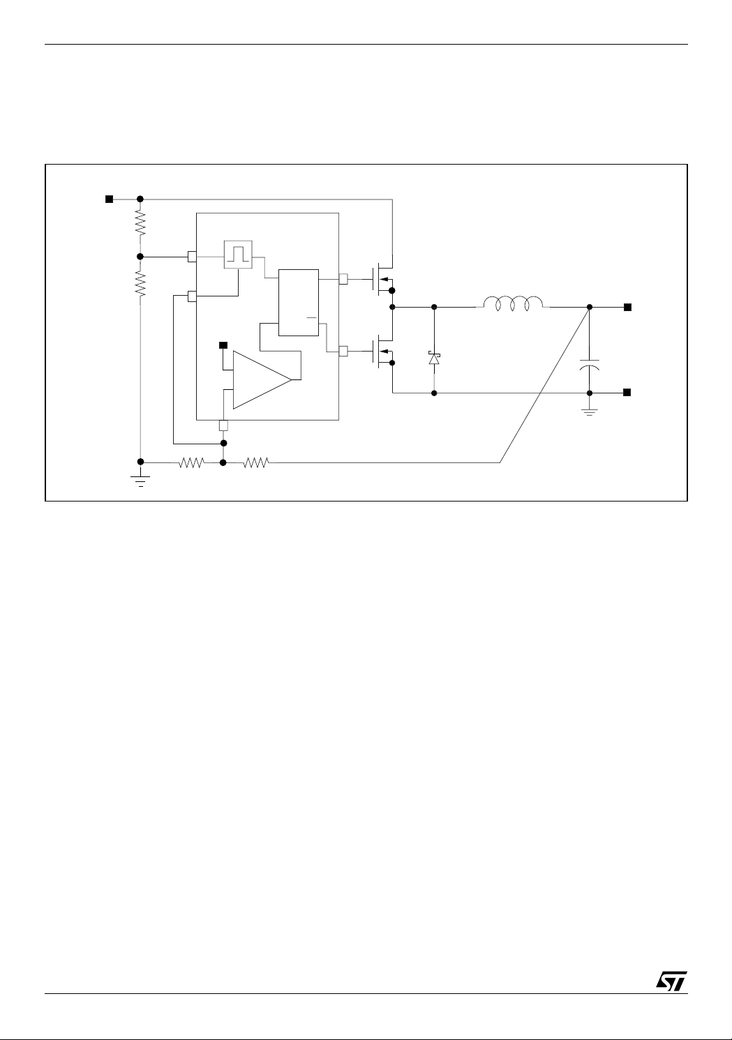
Figure 2. Minimum Component Count Application
Rin1Rin2
VDR
OSC
BOOT
HGATE
PHASE
LGATE
PGND
GND
GNDSENSE
Rilim
VCC
PGOOD
OVP
L6997S
ILIM
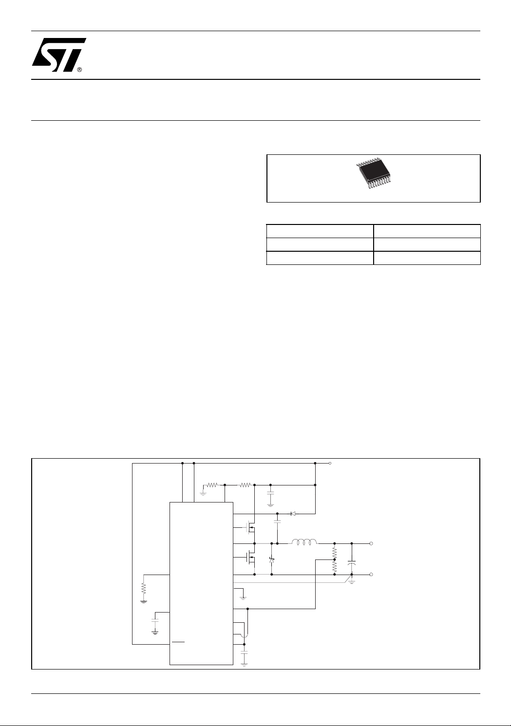
Figure 1. Package
TSSOP20
Table 1. Order Codes
Part Number Package
L6997S TSSOP20
L6997STR Tape & Reel
3 Description
The device is a high efficient solution for networking
dc/dc modules and mobile applications compatible
with 3.3V bus and 5V bus.
It's able to regulate an output voltage as low a s 0.6V.
The constant on time topology assures fast load tran-
sient response. The embedded voltage feed-forward
provides nearly constant switching frequency operation in spite of a wide input voltage range.
An integrator can be introduced in the control loop to
reduce the static output voltage error.
The remote sensing improves the static and dynamic
regulation, recovering the wires voltage drop.
Pulse skipping technique reduces power consumption at light loads. Drivers current capability allows
output currents in excess of 20A.
3.3V
Cin
Dboot
HS
Cboot
L
LS
DS
Ro1
Ro2
0.6V
Cout
June 2004
Css
SS
SHDN
VSENSE
INT
VFB
Vref
Cvref
REV. 1
1/30
L6997S
Table 2. Absolute Maximum Ratings
Symbol Parameter Value Unit
V
CC
V
DR
V
PHASE
BOOT, HGATE
and PHASE
PINS
OTHER PINS ±2000 V
P
tot
T
stg
Table 3. Thermal Data
Symbol Parameter Value Unit
R
th j-amb
T
j
VCC to GND -0.3 to 6 V
V
to GND -0.3 to 6 V
DR
HGATE and BOOT, to PHASE -0.3 to 6 V
HGATE and BOOT, to PGND -0.3 to 42 V
PHASE -0.3-to 36 V
LGATE to PGND -0.3 to V
ILIM, VFB, VSENSE, NOSKIP, SHDN, PGOOD, OVP, VREF,
INT, GND
SENSE
to GND
-0.3 to V
Maximum Withstandin g Voltage Range
+0.3 V
DR
+0.3 V
CC
±750 V
Test Condition:CDF-AEC-Q100-002 “Human Body Model”
Accepatance Criteria: “Normal Performance”
Power dissipation at T
= 25°C 1 W
amb
Storage temperature range -40 to 150 °C
Thermal Resistance Junction to Ambient 125 °C/W
Junction operating temperature range -40 to 125 °C
Figure 3. Pin Connection (Top View)
NOSKIP
GNDSENSE
INT
INT
VSENSE
VCC
GND
VREF
VFB
OSC
20
2
3
4
5
6
7
8
9
10SS
TSSOP20
19
18
17
16
15
14
13
12
11
BOOT1
HGATE
PHASE
VDR
LGATE
PGND
PGOOD
OVP
SHDN
ILIM
Table 4. Pin Function
N° Name Description
1 NOSKIP Connect to V
2 GNDSENSE Remote ground sensing pin
3 INT Integrator output. Short this pin to VFB pin and connect it via a capacitor to V
integrator in the control loop. If the integrator is not used, short this pin to VREF.
4 VSENSE This pin must be connected to the remote output voltage to detect overvoltage and
undervoltage conditions and to provide integrator feedback input.
to force continuous conduction mode and sink mode.
CC
to insert the
OUT
2/30
L6997S
Table 4. Pin Function (continued)
N° Name Description
5VCCIC Supply Voltage.
6 GND Signal ground
7 VREF 0.6V voltage reference. Connect a ceramic capacitor (max. 10nF) between this pin and
8 VFB PWM comparator feedback input. Short this pin to INT pin to enable the integrator function, or
9 OSC Connect this pin to the input voltage through a voltage divider in order to provide the feed-
10 SS Soft Start pin. A 5µA constant current charges an external capacitor. Itsvalue sets the soft-
11 ILIM An external resistor connected between this pin and GND sets the current limit threshold don’t
12 SHDN Shutdown. When connected to GND the device and the drivers are OFF. It cannot be left
13 OVP Open drain output. During the over voltage condition it is pulled up by an external resistor.
14 PGOOD Open drain output. It is pulled down when the output voltage is not within the specified
15 PGND Low Side driver ground.
16 LGATE Low Side driver output.
17 V
DR
18 PHASE Return path of the High Side dr iver.
19 HGATE High side driver output.
20 BOOT Bootstrap capacitor pin. High Side driver is supplied through this pin.
ground. This pin is capable to source or sink up to 250uA
to VSENSE to disable the integrator function.
forward function don’t leave floating.
start time do n’t leave floating.
leave floating..
floating.
thresholds. Otherwise is pulled up by external resistor. If not used it can be left floating.
Low Side driver supply.
Table 5. Electrical Characteristics
(V
= VDR = 3.3V; T
CC
Symbol Parameter Test Condition Min. Typ. Max. Unit
SUPPLY SECTION
Vin Input voltage range Vout=Vref Fsw=110Khz Iout=1A 1 35 V
V
,
CC
V
DR
V
Turn-onvoltage 2.86 2.97 V
CC
Turn-off voltage 2.75 2.9 V
Hysteresis 90 mV
IqV
Drivers Quiescent Current VFB > VREF 7 20 µA
DR
IqVcc Device Quiescent current VFB > VREF 400 600 µA
SHUTDOWN SECTION
SHDN Device On 1.2 V
Device Off 0.6 V
I
SHVDR
I
SHVCC
Drivers shutdown current SHDN to GND 5 µA
Devices shutdown current SHDN to GND 1 15 µA
SOFT START SECTION
I
∆V
Soft Start current VSS = 0.4V 4 6 µA
SS
Active Soft start and voltage 300 400 500 mV
SS
= 0°C to 85°C unless otherwise specified)
amb
35.5V
3/30
L6997S
Table 5. Electrical Characteristics (continued)
= VDR = 3.3V; T
(V
CC
Symbol Parameter Test Condition Min. Typ. Max. Unit
CURRENT LIMIT AND ZERO CURRENT COMPARATOR
I
Input bias current R
LIM
Zero Crossing Comparator offset
Phase-gnd
K
Current limit factor 1.6 1.8 2 µA
ILIM
ON TIME
Ton On time duration V
OFF TIME
T
OFFMIN
Minimum off time 600 ns
K
OSC/TOFFMIN
VOLTAGE REFERENCE
VREF Voltage Accuracy 0µA < I
PWM COMPARATOR
Input voltage offset -2 +2 mV
I
Input Bias Current 20 nA
FB
INTEGRATOR
Over Voltage Clamp V
Under Voltage Clamp V
Integrator Input Offset Voltage
V
SENSE-VREF
I
VSENSE
Input Bias Current 20 nA
GATE DRIVERS
High side rise time V
High side fall time 50 100 ns
Low side rise time V
Low side fall time 50 90 ns
P
UVP/OVP PROTECTIONS
GOOD
OVP Over voltage threshold with respect to V
UVP Under voltage threshold 67 70 73 %
Upper threshold
(V
SENSE-VREF
Lower threshold
(V
SENSE-VREF
V
PGOOD
= 0°C to 85°C unless otherwise specified)
amb
= 2KΩ to 200KΩ 4.655.4µA
ILIM
REF=VSENSE
V
REF=VSENSE
V
REF=VSENSE
V
REF=VSENSE
OSC=125mV 720 800 880 ns
OSC=250mV 370 420 470 ns
OSC=500mV 200 230 260 ns
OSC=1000mV 90 115 140 ns
OSC=250mV 0.20 0.40
< 100µA 0.594 0.6 0.606 V
REF
= V
SENSE
SENSE
DR
CC
= GND 0.45 0.55 0.65 V
=3.3V; C=7nF
HGATE - PHASE from 1 to 3V
=3.3V; C=14nF
DR
LGATE from 1 to 3V
REF
V
rising 110 112 116 %
SENSE
)
V
falling 858891%
SENSE
)
I
=2mA 0.2 0.4 V
Sink
-2 2 mV
0.62 0.75 0.88 V
-4 -4 mV
50 90 ns
50 90 ns
118 121 124 %
4/30
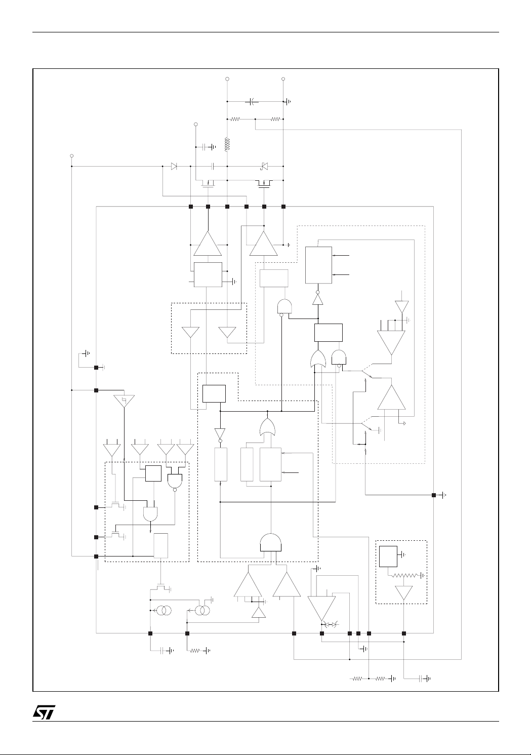
Figure 4. Functional & Block Diagram
IN
V
Vcc
L6997S
OUT
V
GNDVCCOVPPGOODSHDN
overvoltage comparator
VSENSE
+
1.12 VREF
-+undervoltage comparator
VSENSE
0.6 VREF
pgood comparators
SR
LS and HS anti-cross-conduction comparators
VSENSE
1.075 VREF
-
+
comp
V(LGATE)<0.5V
VSENSE
+
BOOT
VCC
0.925 VREF
-
HGATE
HS driver
level shifter
V(PHASE)<0.2V
Q
R
comp
S
Toff min
PHASE
delay
VDR
Ton min
one-shot
PGND
LGATE
LS driver
Q
R
Ton
one-shot
Ton
S
OSC
VSENSE
Q
S
one-shot
OSC
VSENSE
Ton= Kosc V(VSENSE)/V(OSC)
R
no-skipno-skip
mode
mode
comparator
negative current limit
PHASE
++-
-
+
PHASE
ILIM
0.05
zero-cross comparator
LS control
Ton= Kosc V(VSENSE)/V(OSC)
NOSKIP
IC enable
control
soft-start
SS
5 uA
power management
ILIM
comparator
positive current limit
-
PHASE
+-+
+VREF
0.05
FB
HS control
VREF
pwm comparator
-
-
-
+
+
Gm
VREF
INT
VSENSE
IN
V
SENSEGND
OSC
1.236V
bandgap
VREF
1.416
Reference chain
0.6V
5/30
L6997S
4 DEVICE DESCRIPTION
4.1 Constant On Time PWM topology Figure 5. Loop block schematic diagram
Vin
R1
R2
One-shot generator
OSC
Vsense
Vref
FFSR
Q
R
HGATE
S
Q
+
LGATE
HS
LS
Vout
DS
-
PWM comparator
FB
R4
R3
The device implements a Constant On Time control scheme, where the Ton is the high side MOSFET on time
duration forced by the one-shot generator. The On Time is directly proportional to VSENSE pin voltage and inverse to OSC pin voltage as in Eq1:
V
SENSE
T
ON
where K
= 180ns and τ is the internal propagation delay time (typ. 40ns). The system imposes in steady
OSC
state a minimum On Time corresponding to V
responding Ton will not decrease. Connecting the OSC pin to a voltage partition from V
steady-state switching frequency F
V
OUT
-------------- -
f
== =
SW
-----------
T
V
IN
--------------------- -
K
OSC
V
OSC
independent of VIN. It results:
SW
α
1
ON
OSC
-------------- -
α
OUT
τ+=
= 1V. In fact if the V
OSC
1
---------------
K
OSC
α
→ fSWK
OSC
(1)
voltage increases above 1V th e cor-
OSC
OSCαOUT
to GND, it allows a
IN
(2)
where
V
OSC
α
α
OSC
OUT
-------------- -
V
IN
V
FB
-------------- -
V
OUT
The above equations allow setting the frequency divider ratio α
that such equations hold only if V
<1V. Further the Eq2 shows how the system has a switching frequen-
OSC
cy ideally independe nt fr om the i npu t vo lta ge. T h e del ay in tro duc es a ligh t dep end enc e fr om V
R
2
--------------------==
R2R1+
R
4
--------------------==
R3R4+
(3)
(4)
once output voltage has been set; note
OSC
IN
. A mini-
mum Off-Time constraint of about 500ns is introduced in order to assure the boot capacitor charge and to
6/30
L6997S
limit the switchin g frequency after a loa d transient as well as to mask PWM comp arator output again st
noise and spikes.
The system has not an in ternal clock, becau se this is a hys teretic controller, so the turn on pulse wi ll start if thre e
conditions are met contemporarily: the FB pi n voltage i s lower than the r eference volt age, the minimum off time
is passed and the current limit comparator is not triggered (i.e. the inductor current is below the current limit
value). The voltage at the OSC pin must range between 50mV and 1V to ensure the system linearity.
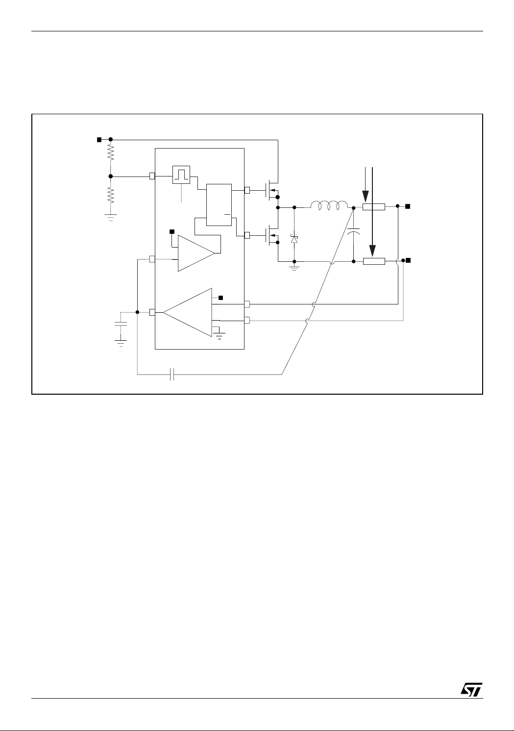
4.2 Closing the loop
The loop is closed connecting the output voltage (or the output divider middle point) to the FB pin. The FB pin
is internally conncted to the comparator negative pin while the positive pin is connected to the reference voltage
(0.6V Typ.) as in Figure 5. When the FB goes lower than the reference voltage, the PWM comparator output
goes high and sets the flip-flop output, turning on the high side MOSFET. This condition is latched to avoid
noise. After the On-Time (calculated as described in the previous section) the system resets the flip-flop, turns
off the high side MOSFET and turns on the low side MOSFET. For more details refers to the Figure 4.
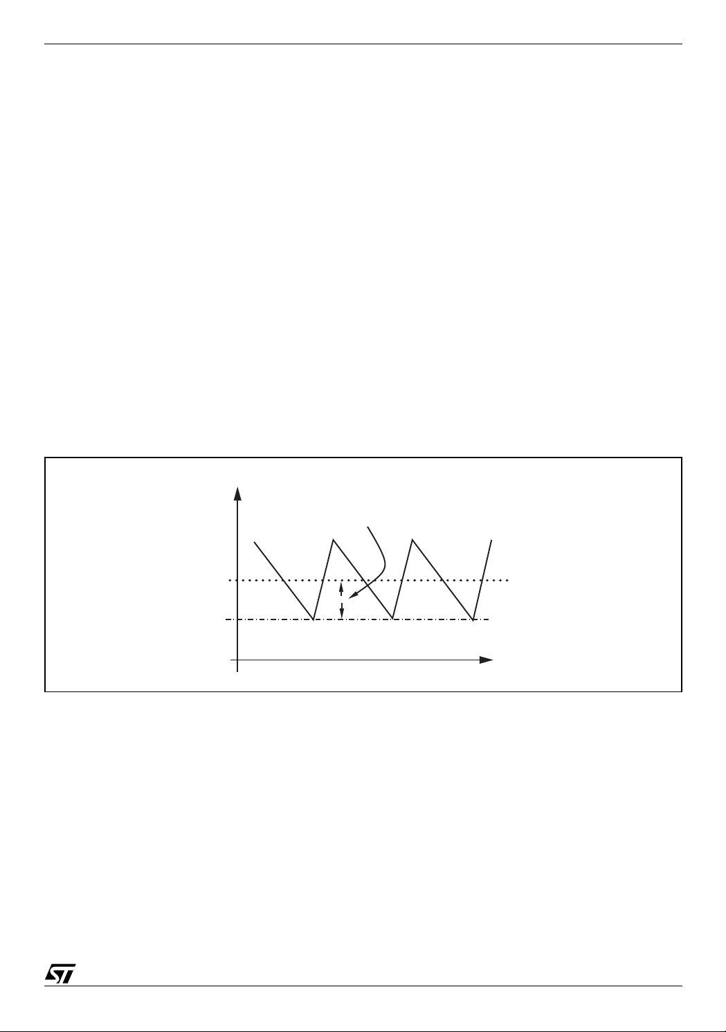
The voltage drop along ground and supply metal paths connecting output capacitor to the load is a source of
DC error. Further the system regulates the output voltage valley value not the average, as shown in Figure 6.
So, the voltage ripple on the output capacitor is a source of DC static error (well as the PCB traces). To compensate the DC errors, an integrator network must be introduced in the control loop, by connecting the output
voltage to the INT pin through a capacitor and the FB pin to the INT pin directly as in Figure 7. The internal integrator amplifier with t he extern al capacitor C
an AC path for output ripple.
introduces a DC pole in the control loop. C
INT1
also provides
INT1
Figure 6. Valley regulation
Vout
DC Error Offset
<Vout>
Vref
Time
The integrator amplifier generates a c urrent, proportional to the DC error s, that increases the output capaci tance
voltage in order to compensate the total st atic error. A v oltage clamp within the devi ce forces anINT pin v oltage
range (V
-50mV, V
REF
+150mV). This is useful to avoid or smooth output voltage overshoot during a load
REF
transient. Also, this means that the integrator is capable of recovering output error due to ripple when its peakto-peak amplitude is less than 150mV in steady state.
In case the ripple amplitude is larger than 150mV, a capacitor C
can be connected between INT pin and
INT2
ground to reduce ripple amplitude at INT pin, otherwise the int egrator will operate out of its linear range. Choose
C
according to the following equation:
INT1
g
⋅
INTαOUT
C
INT1
where g
=50 µs is the integrator transconductance,
INT
the close loop bandwidth. This equation holds if C
-------------------------------=
2 π F
⋅⋅
(5)
u
α
is the output divider ratio given from Eq4 and FU is
OUT
is connected between INT pin and ground. C
INT2
INT2
is given
by:
7/30
L6997S
Where
C
--------------- -
C
∆
V
is the output ripple and ∆V
OUT
INT2
INT1
∆
------------------=
∆V
V
OUT
INT
INT
Figure 7. Integrator loop block diagram
Vin
R1
R2
Cint2
One-shot generator
OSC
From Vsense
Vref
FB
INT
Integrator amplifier
+
-
PWM comparator
+
-
+
(6)
is the required ripple at the INT pin (100mV typ).
PCB TRACES
FFSR
Q
R
HGATE
S
Q
LGATE
Vref
-
Vsense
Gndsense
HS
LS
DS
Vout
LOAD
Cint1
Respect to a traditional P WM con t roller, that has an internal oscil lator s etti ng the switching frequency, i n a hys teretic system the frequency can change with some parameters. Fo r example, while in a standard fixed s witc hing frequency topology, the increase of the losses (increasing the output current, for example) generates a
variation in the On Time and Off Time, in a fixed On Time topology , the increase of the losses generates only
a variation on the Off Time, changing the switching frequency. In the device is implemented the voltage feedforward circuit that allows constant swi tchi ng fr equency during s teady -sate oper atio n and withi nthe inp ut rang e
variation. Any way there are many factors affecting switching frequency accuracy in steady-state operation.
Some of these are internal as dead times, which depends on high side MOSFET driver. Others related to the
external components as high side MOSFET gate charge and gate resistance, voltage drops on supply and
ground rails, low side and high side RDSON and inductor parasitic resistance.
During a positive load transient, (the output current increases), the conve rter switches at its maximum frequency
(the period is TON+TOFFmin) to recover the output voltage drop. During a negative load transient, (the output
current decreases), the device stops to switch (high side MOSFET remains off).
4.3 Transition from PWM to PFM/PSK
To achieve high efficie ncy at light loa d conditi ons, PFM mode i s provided. The PFM mode differs fr om the PWM
mode essentially for the off phase; the on phase is the same. In PFM after a On cycle the system turns-on the
low side MOSFET until the inductor current goes down zero, when the zero-crossing comparator turns off the
low side MOSFET. In PWM mode, after On cycle, the system keeps t he low side MOSFET on unti l the next turnon cycle, so the energy stored in the output capacitor will flow through the low side MOSFET to ground. The
PFM mode is naturally implemented in an hysteretic controller enabling the zero current comparator by enabling, in fact in PFM mode the system reads the output voltage with a comparator and then turns on the high
side MOSFET when the output voltage goes down to reference value. The device wor ks in discontinuous mod e
8/30
L6997S
at light load and in continuous mode at high load. The transition from PFM to PWM occu rs when load curr ent is
around half the inductor current ripple. This threshold value depends on V
the inductor value is, the smaller the threshold is. On the other hand, the bigger the i nductor value is, the sl ower
the transient response is. The PFM waveforms may appear more noisy and asynchronous than normal operation, but this is normal behaviour mai nly due to the ver y low loa d. If the PFM i s not c ompati ble wi th the appl ic ation it can be disabled connecting to V
the NOSKIP pin.
CC
4.4 Softstart
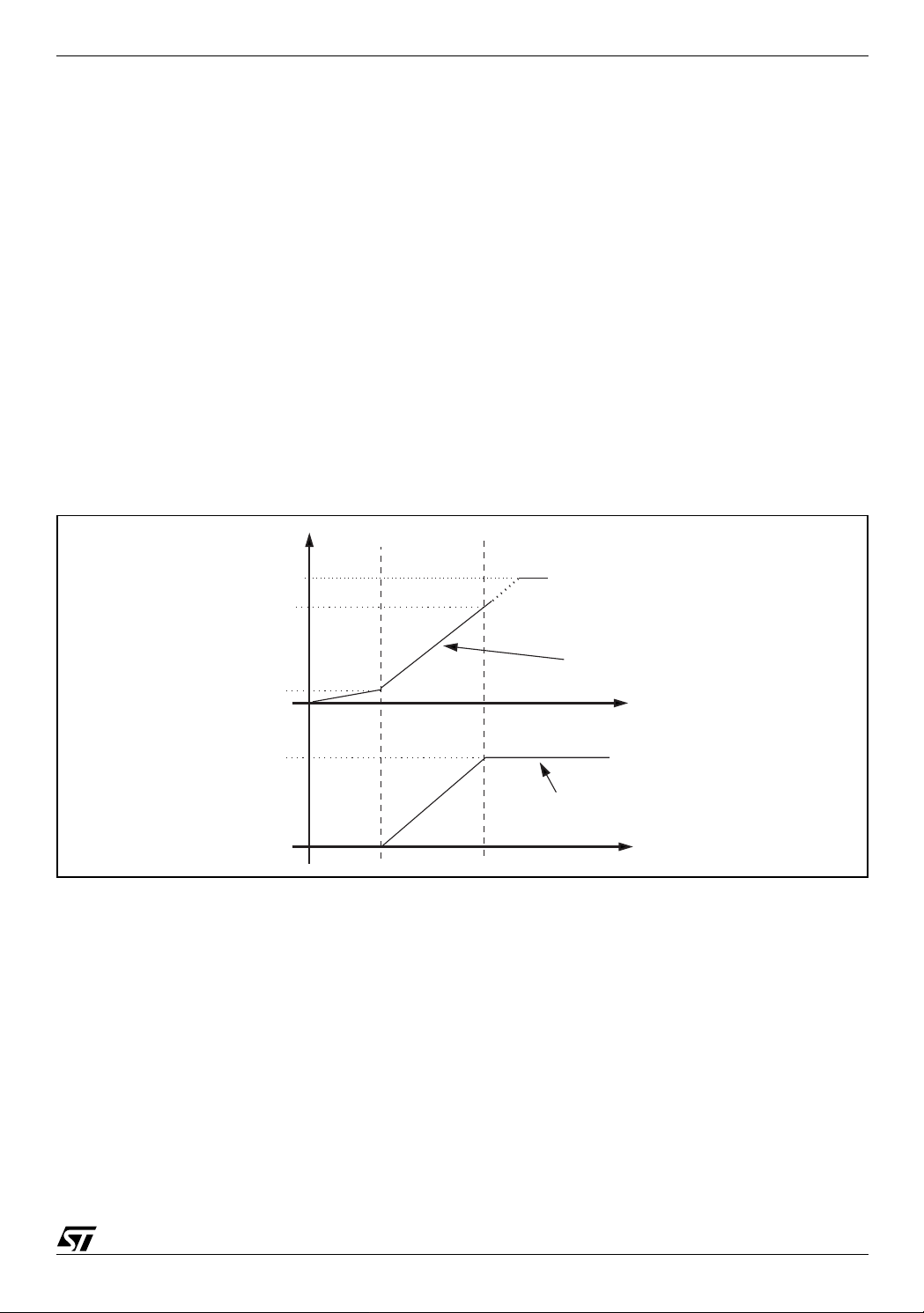
After the device is turned on the SS pin voltage begin s to increase and the system star ts to switch. The softstart
is realized by gradually increasing the current limit threshold to avoid output overvoltage. The active soft start
range for the V
internal current source (5
voltage (where the output current limit increase linearly) is from 0.6V to 1V. In this range an
SS
µ
A Typ) charges the capacitor on the SS pi n; the reference curr ent (for the current li mit
comparator) forced through ILIM pin is proportional to SS pin voltage and it saturates at 5
voltage is close to 1V the maximum current lim it is active. Output protecti ons OVP & UVP are disab led until the
SS pin voltage reaches 1V (see figure 8).
Once the SS pin voltage reaches the 1V value, the voltage on SS pin doesn't impact the system operatio n anymore. If the SHDN pin is turned on before the supplies, the power section must be turned on before the logic
section. While if the supplies are applied with the SHND pin off, the start up sequence doesn't meter.
Figure 8. Soft -Start Diagram
Vss
, L, and V
IN
. Note that the higher
OUT
µ
A (Typ.). When SS
4.1V
1V
0.6V
Ilim current
5
A
µ
Soft-start active range
Time
Maximum current limit
Time
Because the system implements the s oft s tart by contr ol lin g the inductor current, the soft star t capac itor s houl d
be selected based on of the output capacitance, the current limit and the soft start active range (
∆
VSS).
In order to select the softstart capacitor i t must be imposed that the output voltage reaches the final value before
the soft start voltage reaches the under voltage value (1V). After this UVP and OVP are enable.
The time necessary to charge the SS capacitor up to 1V is given by:
1V
TSSCSS()
--------
Iss
CSS⋅=
(7)
In order to calculate the output voltage chargin time it should be considered that the inductor current function
can be supposed linear function of the time.
t,CSS()
I
L
R
ilim/RdsonKILIMISS
-------------------------------------------------------------------------- -=
V
⋅∆()
SSCSS
t⋅⋅⋅()
(8)
9/30

L6997S
so considering zero the output load the output voltage is given by:
V
out
t,CSS()
------------------------ -
Qt,C
()
SS
C
out
-----------------------------------------------------------------------------==
R
ilim/RdsonKILIMISS
C
out
⋅⋅⋅()
VSSCSS2⋅⋅∆⋅()
2
t
(9))
indicating with V
the minimum C
the final value, the output charging time can be estimated as:
out
V
outCout
--------------------------------------------------------------------------- -
V
()
outCSS
value is given imposing this condition:
SS
=
R
ilim/RdsonKILIMISS
T
=T
out
V
SSCSS
⋅⋅()
SS
0.5
2⋅⋅∆⋅⋅()
(10)
(11)
4.5 Current limit
The current limit comparator s enses the inductor current through the lo w si de MOSFET RDSON drop and compares this value with the ILIM pin voltage value. While the current is above the current limit value, the control
inhibits the high side MOSFET Turn On.
To properly set the current limit threshold, it sho uld be noted that thi s i s a valley cur rent li mit. The Av er age cur rent depends on the inductor value, V
IN VOUT
and switching frequency.
The average output current in current limit is given by:
I∆
I
OUT
CL
I
max va lley
---- -+=
(12)
2
Thus, to set the current threshold, choose RILIM according to the following equation:
R
ILim
I
max valley
-----------------
Rds
on
⋅=
K
(13)
ILIM
In overcurrent conditions the syst em keeps the current constant until the output v oltage meets the undervoltag e
threshold. The negative valley current lim it, for t he sink mode, is set automati cally at the same va lue of the positive valley current limit. The average negative current limit differs from the positive average current limit by the
ripple current; this difference is due to the valley control technique.
The current limit system accuracy is function of the precision of the resistance connected to the ILIM pin and
the low side MOSFET RDS
accuracy. Moreover the voltage on ILIM pin must range between 10mV and 1V
ON
to ensure the system linearity.
Figure 9. Current limit schematic
Positive and negative current limit
10/30
To inductor
LS
PGN
R
ILIM
D
Current
Comparator
5µA
PHASE
To
logic

L6997S
4.6 Protection and fault
The load protection is realized by using the VSENSE pin. Both OVP and UVP ar e latched, and the fault conditio n
is indicated by the PGOOD and the OVP pins. If the output voltage is between the 89% (typ.) and 110% (typ)
of the regulated value, PGOOD is high. If a hard overvoltage or an undervoltage occurs, the device is latched:
low side MOSFET and, high side MOSFET are turned off and PGOOD goes low. In case the system detects a n
overvoltage the OVP pin goes high.
To recover the functionality the device must be shut down and restarted the SHDN pin, or by remov ing the supply, and restarting the devicewith the correct sequence.
4.7 Drivers
The integrated high-current drivers allow using different size of power MOSFET, maintaining fast switchi ng transitions. The driver for the high side MOSFET uses the BOOT pin for supply and PHASE pin for return (floating
driver). The driver for the low side MOSFET uses the VDR pin for the supply and PGND pin for the return. The
drivers have the adaptive anti-cross-conduction protection, which prevents from having bothhigh side and low
side MOSFET on at the same time, avoi ding a high current to flow from VIN to GND. When high s ide MOSFET
is turned off the voltage on the PHASE pin begins to fall; the low side MOSFET is turned on only when the voltage on PHASE pin reaches 250mV. When low side is turned off, high side remains off until LGATE pin voltage
reaches 500mV. This is important since the driv er can work properly wi th a l arge range of external po wer MOSFETS.
The current necessary to switch the external MOSFETS flows through the device, and it is proportional to the
MOSFET gate charge the switching frequency and the driver voltage. So the power dissipati on of the devic e is
function of the external power MOSFET gate charge and switching frequency.
P
driver
VccQ
⋅⋅=
gTOTFSW
(14)
The maximum gate charge values for the low side and high side are given by:
f
SW0
Where f
Q
MAXHS
Q
MAXLS
= 500Khz. The equations above are valid for TJ = 150°C. If the system temperature is lower the Q
SW0
------------ -
f
SW
f
SW0
------------ -
f
SW
75nC⋅=
125nC⋅=
(15)
(16)
can be higher.
For the Low Side driver the max output gate charge meets another limit due to the internal traces degradation;
in this case the maximum value is Q
MAXLS
= 125nC.
The low side driver has been designed to have a low resistance pull-down transistor, approximately 0.5 ohms.
This prevents undesired LS MOSFET Turn On during the fast rise-time of the pin PHASE, due to the Miller effect.
When the 3.3V bus is used to supply the drivers, ULTRA LOGIC LEVEL MOSFETs should be selected , to be
sure that the MOSFETs work in properly way.
G
11/30

L6997S
5 APPLICATION INFORMATION
5.1 5A Demo board description
The demo board shows the device operation in this condition: VIN from 3.3V to 5V, I
evaluation board let use the system wi th 2 diffe rent volta ges ( V
the supply for the IC and VIN the power input
CC
for the conversion) so replacing the input capacitors the power input voltage could be also 35V. When instead
the input voltage (V
) is equal to the VCC it should be better joinin g them wi th a 10Ω resistor in order to filter the
IN
device input voltage. On the topside demo there are two different jumpers: one jumper, near the OVP and POWER GOOD test points, is used to shut down the device; when the jumper is present the device is in SHUTDOWN
mode, to run the device remove the jumper. The other jumper, near the V
test point, is used to set the PFM/
REF
PSK mode. When the jumper is present, at l ight load, the sy stem will go in PFM mode; if there i s not the jumper,
at light load, the syst em will remai n in PWM mo de. In the demo bottom si de there are two others di fferent j umpers. They are used to set or remove the INTEGRATOR configuration. When the jumpers named with INT label
are closed AND the jumpers named with the NOINT label are open the integrator configuration is set. Sometimes the integrator configuration needs a low frequency filter the to reduce the noise interaction. In this case
instead close the INT jumper s put there a r esistor and after a capaci tor to ground ( as in the s chematic diagram) ;
the pole value is around 500Khz but it should be higher enough than the switching frequency (ten times). On
the opposite when the jumpers named with the NOINT are closed and the jumpers named with INT are open
the NON INTEGRATOR configuration is selected. Refer to the Table 1 and 2 for the jumpers connection.
Figure 10. Demoboard Schematic Diagram
OUT
=5A V
=1.25V. The
OUT
Vcc
TP1
TP2
R9
R5
SD
R8
C9
C11
R10
C12
C10
R7
VCC
PGOOD
OVP
L6997S
ILIM
SS
SHDN
VDR
C8
R4
OSC
BOOT
HGATE
PHASE
LGATE
PGND
GND
NOSKIP
VSENSE
GNDSENSE
INT
VFB
VREF
C6
C5
R6
Q1
Q2
NOINT
TP3
C4
NOINT
INT
D2
C2
C7,C13
D1
R1
C1
NS
Cn
J1
VIin
GNDin
L1
C14,C15
C3
INT
Rn
VOUT
R3
R2
GNDOUT
12/30

5.2 Jumper Connection Table 6. Jumper connection with integrator
Component Connection
C1 Mounted
C2 Mounted *
INT Close
NOINT Open
* This component is not necessary, depends from the output ESR capacit or. See the integrator section.
Table 7. Jumper connection without integrator
Component Connection
C1 Not mounted
C2 Not Mounted
INT Open
NOINT Close
5.3 DEMOBOARD LAYOUT
Real dimensions: 4,7 cm X 2,7 cm (1.85 inch X 1. 063 inch)
L6997S
Figure 11. Top side components placement
Figure 12. Bottom side Jumpers distribution
Figure 13. Top side layout
Figure 14. Bottom side layout
13/30

L6997S
Table 8. PCB Layout guidelines
Goal Suggestion
To minimize radiation and magnetic
coupling with the adjacent circuitry .
To maximize the efficiency. Keep power traces and load connections short and wide.
To ensure high accuracy in the
current sense system.
To reduce the noise effect on the IC. 1) Put the feedback component (like output divider, integrator network, etc) as
1) Minimize switching current loop areas. (For example placing C
and Low side MOSFETS, Shottky diode as close as possible).
2) Place controller placed as close as possible to the power MOSFETs.
3) Group the gate drive components (Boot cap and diode) near the IC.
Make Kelvin connection for Phase pin and PGND pin and keep them as close
as possible to the Low Side MOSFETS.
close as possible to the IC.
2) Keep the feedback traces parallel and as close as possible. Moreover they
must be routed as far as possible from the switching current loops.
3) Make the controller ground connection like the figure 8.
, High Side
IN
Table 9. Component list
The component list is shared in two sections: the first for the general-purpose component, the second for
power section:
Part name Value Dim en sio n Notes
GENERAL-PURPOSE SECTION
RESISTOR
R1, R5, R9, R10 33kΩ 0603 Pull-up resistor
R2 1kΩ 0603 Output resistor divider (To set output voltage)
R3 1.1kΩ 0603
R4 0603 Input resistor divider (To set switching frequency)
R6 470kΩ 0603
R7 0Ω 0603
R8 0603 Current limit resistor
CAPACITOR
C1 330pF 0603 First integrator capacitor
C2 N.M. 0603 Second integrator capacitor
C3 1nF 0603
C4 100nF 0603
C5 1µFTantalum
C6 10nF 0603
C9 10nF 0603 Softstart capacitor
C10 100nF 0603
C11 100nF 0603
C8, C12 47pF 0603
DIODE
D1 BAR18
POWER SECTION
INPUT CAPACITORS
C7, C13 47µF ECJ4XF0J476Z
PANASONIC
14/30

L6997S
Table 9. Component list (continued)
The component list is shared in two sections: the first for the general-purpose component, the second for
power section:
Part name Value Dim en sio n Notes
OUTPUT CAPACITORS
C14, C15 220µF 2R5TPE220M
POSCAP
INDUCTOR
L1 2.7 µH DO3316P-272HC
POWER MOS
Q1,Q2 STS5DNF20V STMicroelectronics Double mosfet in sigle package
DIODE
D2 STPS340U STMicroelectronics 3
Notes: 1. N.M.=Not Mounted
2. The demoboard with this component list is set to give: V
3.3V-5V and with the integrator feature.
3. The diode efficiency impact is very low; it is not a nec essary component.
4. All cap acitors are intended ceramic type otherwise specified.
COILCRAFT
OUT
= 1.25V, FSW = 270kHz with an input voltage around VIN = VCC =
5.4 EFFICIENCY CURVES Source mode
V
= 3.3V V
IN
= 1.25V F
OUT
= 270kHz
SW
Figure 15. Efficiency vs output current
E ff [%]
100,0
90,0
80,0
70,0
60,0
50,0
40,0
30,0
20,0
10,0
0,0
0,0 1,0 2,0 3,0 4,0 5,0 6,0
PFM mode PWM mode
Cu rren t [ A]
15/30

L6997S
6 STEP BY STEP DESIGN
Application conditions: VIN = 3.3V, ±10% V
6.1 Input capacitor.
A pulsed current (with zero average value) flows through the input capacitor of a buck converter. The AC component of this current is quite high and dissipates a considerable amount of power on the ESR of the capacitor:
P
CIN
ESR
CIN
⋅⋅=
The RMS current, which the capacitor must provide, is given by:
OUT
Iout
= 1.25V I
2
Vin Vin Vout–()⋅
----------------------------------------------- -
OUT
Vin
2
= 5A FSW = 270kHz
(17)
2
I
∆()
L
(18)
Where
Icin
rms
δ
is the duty cycle of the application
Iout2δ 1 δ–()
δ
------
+=
12
Neglecting the last term, the equation reduces to:
Icin
which maximum value corresponds to to
rms
Iout δ 1 δ–()=
δ
= 1/2 and is equal I
(19)
out
/2
Therefore, in worst case, the input capacitors should be selected with a RMS ripple current rating as high as
half the respective maximum output current.
Electrolytic capacitors are the most used because theyare the cheapest ones and are available with a wide
range of RMS current ratings. The only drawback is that, for a givenripple cu rrent rating, they are physically larger than other capacitors. Very good tantalum capacitors are comi ng available, with very low ESR and s mall size.
The only problem is that they occasionally can burn i f subjected to v ery high c ur rent duri ng the char ge. So, i t is
better avoid this type of capacitors for the input filter of the device. In fact, they can be subjected to high surge
current when connected to the power supply. If availabl e for the requested capacitance value and vo ltage rating,
the ceramic capacitors have usually a hig her RMS current r ating for a given ph ysical di mension (due to the very
low ESR). The drawback is the quite high cost. Possible solutions:
10µF C34Y5U1E106ZTE12 TOKIN
22µF JMK325BJ226MM
47µF ECJ4XF0J476Z
33µF C3225X5R0J476M
TAIYO-YUDEN
PANASONIC
TDK
With our parameter from the equation 3 it is found:
Icin
= 2.42A
rms
6.2 Inductor
To define the inductor, it is necessary to determine firstly the inductance value. Its minimum value is given by:
where RF =
16/30
V
Lmin
∆
I/I
(basically it is approximately 30%).
OUT
-------------------------------------------------------------- -
≥
F
SWIout
Vin
o
–()⋅
maxVo
RF Vin
⋅⋅⋅
(20)
max

L6997S
With our parameters:
Lmin
≥ 2µ
H
The saturation current must be higher then 5A
6.3 Output capacitor and ripple voltage
The output capacitor is selected based on both static and dynamic output voltage accuracy. The static output
voltage accuracy depends mostly on the ERS of the output capacitor, while the dynamic accuracy usually depends both on the ESR and capacitance value.
If the static precision is ±1% for the 1.25V output voltage, the output ripple is ±12.5mV.
To determine the ESR value from the output precision is necessary to calculate the ripple current:
Where F
= 270kHz.
SW
I∆
Vin Vo–
---------------------- -
L
⋅⋅=
Vo
---------
Vin
T
(21)
sw
From the Eq. above the ripple current is around 1.25A.
So the ESR is given by:
ESR
ripple
---------------------
---- -
2
25mV
----------------= 20mΩ==
I∆
1.25
(22)
V
∆
The dynamic specifications are sometimes more relaxed than the static requir ements , Any way a mi nimum output capacitance must be ensur ed to avoid output voltage variation due to the charge an d discharge of Cout dur ing load transients.
To allow the device control loop to work properly, the zero introduced by the output capacitor ESR (
τ
= ESR ·
Cout) must be at least ten times smaller than switching frequency. Low ESR tantalum capacitors, which ESR
zero is close to ten kHz, are suitable for output filtering. Output capacitor value C
and its ESR, ESRC
OUT
OUT
should be large enough and small enough, respec tively, to keep o utput voltage within the accuracy range during
a load transient, and to give the device a minimum signal to noise ratio.
The current ripple flows through the output capacitors, so the should be calculated also to sustain this ripple:
the RMS current value is given by Eq. 18.
1
Icout
rms
---------- -
23
(23)
I
∆=
L
,
But this is usually a negligible constrain.
Possible solutions:
330µF EEFUE0D331R
PANASONIC
220µF2R5TPE220M
POSCAP
Multilayer capacitors can not be used because their very low ESR.
6.4 MOSFET’s and Schottky Diod es
A 3.3V bus powers the gate drivers of the device, the use ultra low level MOSFET is highly recommended, especially for high current applications. The MOSFET breakdown voltage V
must be greater than VINMAX
BRDSS
with a certain margin.
The RDS
can be selected once the allowable power dissipation has been established. By selecting identical
ON
17/30

L6997S
Power MOSFET for us and ls, the total power they dissipate does not depend on the duty cycle. Thus, if PON
is this power loss (few percent of the rated output power), the required
RDS
α
admitted temperature rise. It is worth noticing, however, that generally the lower RDS
charge Q
from the input source to ground, resulting in an equivalent drive current:
(@ 25 °C) can be derived from:
ON
P
RDS
ON
------------------------------------------------ -=
ON
(24)
Iout21 α T∆⋅+()⋅
is the temperature coefficient of RDSON (typically, α = 510-3 °C-1 for these low-voltage classes) and T the
, the higher is the gate
, which leads to a higher gate drive consumption. In fact, each switching cycle, a charge QG moves
G
ON
Iq Qg F
⋅=
SW
(25)
A SCHOTTKY diode can be added to increase the system efficiency at high switching frequency (where the
dead times could be an important part of total switching period).
This optional diode must be placed in parallel to the synchronous rectifier must have a reverse voltage VRRM
greater than VIN
. The current size of the diode must be selected in order to keep it i n safe operati ng condi -
MAX
tions. In order to use l ess space than pos sible, a do uble MOSFET in a single packag e is chos en: STS5DNF20V
6.5 Output voltage setting
The first step is choosing the output divider to set the output voltage. To select this value there isn't a criteria,
Ω
but a low divider network value (around 100
network (100K
R3 = 1K
R2 = 1.1K
Ω
) increase the noise effects. A network divider values from 1KΩ to 10KΩ is right. We chose:
Ω
Ω
) decries the efficiency at lo w current; ins tead a high v alue divi der
The device output voltage is adjustable by connecting a voltage divider from output to VSENSE pin. Minimum
output voltage is V
=VREF=0.6V. Once output divider and frequency divider have been designed as to obtain
OUT
the required output voltage and switching frequency, the following equation gives the smallest input voltage,
which allows L6997S to regulate (which corresponds to T
δ 1
α
OSC
-------------- -
α
OUT
--------------------------------------------- -
⋅–<
------------------------- -
T
1
K
OSC
OFF,MIN
MAX
OFF=TOFFMIN
):
(26)
6.6 Voltage Feedforward
From the equations 1,2 and 3, choosing the switching frequency of 270kHz the resistor divid er can be selected.
For example:
R3 = 470K
R4 = 8.5K
Ω
Ω
6.7 Current limit resistor
From the equation 8 the valley current limit can be set considering the RDSON STS5DNF20V and I
R8 = 120K
Ω
CIR
= 5A:
6.8 Integrator capacit or
Let’s assume FU = 15kHz, V
Since V
= 0.6V, from equation 2, of the device description, it follows αOUT = 0.348 and, from equation 5 it
REF
= 1.25V.
OUT
follows C = 250pF. The output ripple is around 22mV, so the system doe sn't need the secon d integrator capacitor.
18/30

L6997S
6.9 Soft start capacitor
Considering the soft start equations (Eq. 11) at page 10, it can be found:
C
= 150pF
SS
The equations are valid without load. When an ac tive load is present the equations resul t more complex ; further
some active loads have unexpected effect, as higher current than the expected one during the soft start, can
change the start up time.
In this case the capacitor value can be selected on the application; anyway the Eq11 gives an idea about the
C
value.
SS
6.10Sink mode
Figure 16. Efficiency vs output current
Eff [%]
100,0
90,0
80,0
70,0
60,0
50,0
40,0
30,0
20,0
10,0
0,0
0,01,02,03,04,05,0
Current [A]
7 15A DEMO BOARD DESCRIPTION
The evaluation board shows the device operation in these conditions: VIN = 3.3V V
= 200KHz without the integrator feature. The evaluation board has two di fferent input voltages: VCC [from 3V to
5.5V] used to supply the device and the V
er components configuration (C
, C
IN
[up to 35V] for the power conversion. In this way, changing the pow-
IN
, MOSFETs, L) it is possible evaluate the device performance in differ-
OUT
ent conditions. It is also possible to mount a linear regul ator on board used to generate the V
are also present two switches and four jumpers. The two switches have different goals: the one nearest to the
V
is used to turn on/off the device when the VCC and VIN are both present; the other one, near to R11 is used
CC
to turn on/off the PFM feature. The device can be turned on also with the power supply, but a correct start up
sequence is mandatory. V
has to be raised first and then the VCC can be applied too. If the correct sequence
IN
is not respected the device will not start up. The jumpers are used to set the integrator feature and to use the
remote sensing; for more info rmation refers to the Jumpers table. Sometimes when using the integrat or configuration a low frequency filter is required in order to reduce the noise interaction. The pole value should be at
least five times higher than the switching frequency. The low pass filter should be inserted in this way: the resistor, in the place of the INT jumper position and the capacitor between the resistor and ground (refers to the
schematic).
= 1.8V I
OUT
= 15A, F
OUT
. On the top side
CC
SW
19/30

L6997S
OU
Figure 17. L6997S Schematic diagram
C2
SW1
R12
TP1
R11
R7
C21
R6
TP2
C20
R8
C3
VCC
OSC
SS
L6997S
L6997
SHDN
NOSKIP
OVP
PGOOD
GND
R5
VDR
BOOT
HGATE
PHASE
GNDSENSE
LGATE
PGND
VSENSE
INT
VREF
FB
C22
D1
C19
Q4, Q5, Q6
C6
NOINT
INT
R3
R4
Q1, Q2, Q3
D2
NOINT
TP3
C25
C5
L
C7 C8 C9
C10, C11
C12
VCC
C13, C14, C15,
C16, C17, C18
R9
R10
C4
C7
R13
Vin
V
T
C23
C24
INT
R
C
7.1 UMPERS CONNECTION
Table 10. Jumper connection with integrator
Component Connection
C4 Mounted
C7 Mounted*
INT Close
NOINT Open
*This component is not necess ary, depends from the output ESR capacitor. See the integrator sec tion.
Table 11. Jumper connection without integrator
Component Connection
C4 Not mounted
C7 Not Mounted
INT Open
NOINT Close
20/30

7.2 DEMO BOARD LAYOUT
Real dimensions: 5.7cm x 7.7cm (2.28inch x 3. 08inch)
L6997S
Figure 18. PCB layout: bottom side
Figure 19. PCB Layout: Top side
Figure 20. Internal ground plane
Figure 21. Power & signal plane
Table 12. PCB Layout guidelines
Goal Suggestion
To minimize radiation and magnetic
coupling with the adjacent circuitry .
To maximize the efficiency. Keep power traces and load connections short and wide.
To ensure high accuracy in the
current sense system.
To reduce the noise effect on the IC. 1) Put the feedback component (like output divider, integrator network, etc) as
1) Minimize switching current loop areas. (For example placing C
and Low side MOSFETS, Shottky diode as close as possible).
2) Place controller placed as close as possible to the power MOSFETs.
3) Group the gate drive components (Boot cap and diode) near the IC.
Make Kelvin connection for Phase pin and PGND pin and keep them as close
as possible to the Low Side MOSFETS.
close as possible to the IC.
2) Keep the feedback traces parallel and as close as possible. Moreover they
must be routed as far as possible from the switching current loops.
3) Make the controller ground connection like the figure 8.
, High Side
IN
21/30

L6997S
Table 13. Component list
The component list is shared in two sections: the first for the general-purpose component, the second for
power section:
Part name Value Dimension Notes
GENERAL-PURPOSE SECTION
RESISTOR
R1 N.M. 0603 Output resistor divider for the linear regulator.
R2 N.M. 0603
R3 560kΩ 0603 Input r esi sto r div ide r (To set switchin g fre que ncy)
R4 5.6kΩ 0603
R5 47Ω 0603
R6, R7, R11, R12 33kΩ 0603
R8 62kΩ 0603 Current limit resistor (To set current limit)
R9 2.7kΩ 0603 Output resistor divider (To set output voltage)
R10 1.3kΩ 0603
R13 220Ω 0603
CAPACITOR
C1 220nF 0805
C2 47µF KEMET-16V
C3 220nF 0805
C4 150pF 0603 First integrator capacitor
C5 47pF 0603
C6 10nF 0603
C7 N.M. 0603 Second integrator capacitor
C19 220nF 0805
C20 220nF 0603 Softstart capacitor
C21 47pF 0603
C22 220nF 0805
C23 0603 N.M.
C24 1nF 0603
C25 1µFTantalum
DIODES
D1 BAT54 25V
POWER SECTION
OUTPUT CAPACITORS
C11-C12 2X680µF T510x687(1)004AS
INPUT CAPACITORS
C13, C14, C16, C17,
C15 C18
INDUCTOR
L1 1.8µH ETQF6F1R8BFA
POWER MOS
Q1,Q2 SI4442DY VISHAY Siliconix Q3 N.M.
Q5,Q6 SI4442DY VISHAY Siliconix Q4 N.M.
INTEGRATED CIRCUIT
U1 L6997S
100µF ECJ5YF0J1072
47µF ECJ5YF1A4767
KEMET
PANASONIC
PANASONIC
PANASONIC
Output capacitor C8, C9, C10 N.M.
Input capacitor
22/30

7.3 EFFICIENCY CURVES Figure 22. Efficiency vs output Current
100
95
90
85
Efficiency (%)
Vcc=Vin=3.3V
80
Fsw=200KHz
75
0 1 2 3 4 5 6 7 8 9 10 11 12 13 14 15 16
Output Current (A)
L6997S
Vout=2.5V
Vout=1.8V
Vout=1.5V
Vout=1.2V
Vout=0.9V
Table 14. Efficiency Curves For Different Applications (V
up to 25V)
IN
Part name Value Dimension Notes
GENERAL-PURPOSE SECTION
RESISTOR
R1 100Ω 0603 Output resistor divider for the linear regulator.
R2 300Ω 0603
R3 560kΩ 0603 Input resistor divider (To set switching frequency)
R4 10kΩ 0603
R5 47Ω 0603
R6, R7, R11, R12 33kΩ 0603
R8 47kΩ 0603 Current limit resistor (To set current limit)
R9 2,7kΩ 0603 Output resistor divider (To set output voltage)
R10 1kΩ 0603
R13 220Ω 0603
CAPACITOR
C1 220 nF 0805
C2 47µFKEMET-16V
C3 220nF 0805
C4 150pF 0603 Fir st inte grator capa cit or
C5 47pF 0603
C6 10nF 0603
C7 330pF 0603 Second integrator capacitor
C19 220nF 0805
C20 10nF 0603 Softstart capacitor
C21 47pF 0603
C22 220nF 0805
C23 0603 N.M.
23/30

L6997S
Table 14. Efficiency Curves For Different Applications (VIN up to 25V) (continued)
Part name Value Dimension Notes
C24 1nF 0603
C25 1µFTantalum
DIODES
D1 BAT54 25V
POWER SECTION
OUTPUT CAPACITORS
C11-C12 2X100µF B45197-A3107-
K409
EPCOS
INPUT CAPACITORS
C13, C14, C16,
C17, C15 C18
10µF C34Y5U1E106Z
TOKIN
10µF C3225Y5V1E106Z
TDK
10µF ECJ4XF1E106Z
PANASONIC
10µF TMK325F106ZH
TAIYO YUDEN
INDUCTOR
L1 3 µH T50-52 Core, 7T
AWG15
POWER MOS
Q1,Q2 STS11NF3LL STMicroelectronics Q3 N.M.
Q5,Q6 STS11NH3LL STMicroelectronics Q4 N.M.
DIODES
D2 STPS2L25U STMicroelectronics 25V
INTEGRATED CIRCUIT
U1 L6997S
NOTE: For the 25V to 12V conversi on the inductor used is: 77120A core 7T.
Output capacitor C8, C9, C10 N.M.
Input capacitor
7.4 EFFICIENCY CURVES Figure 23. Efficiency vs output Current Figure 24. Efficiency vs output Current
100
95
90
85
Efficiency (%)
80
75
Vin = Vcc = 5V
70
Fsw = 200KHz
65
0 1 2 3 4 5 6 7 8 9 10 11 12 13 14 15 16 17 18 19 20 21
Output Current (A)
24/30
Vo = 3.3V
2.5V
1.8V
1.5V
1.2V
0.9V
100
95
90
85
80
75
70
Efficiency (%)
65
60
55
50
012345678910111213141516171819
Vin = 12V
Vcc = 5V
Fsw = 200KHz
Output Current (A)
Vo = 5V
3.3V
2.5V
1.8V
1.5V
1.2V
0.9V

L6997S
Figure 25. Efficiency Vs Output Current Figure 26. Efficiency Vs Output Current
100
= 5V
V
OUT
= 3.3V
V
OUT
Eff [%]
95
90
85
80
75
= 12V
V
OUT
70
65
V
= 25V
60
55
50
0 1 2 3 4 5 6 7 8 9
IN
VCC= 5V
FSW= 200KHz
Output Current [A]
10 11 12 13 14 15 16
7.5 DDR MEMORY AND TERMINATION SUPPLY
Double data rate (DDR) memories require a particular Power Management Architecture. This is due to fact that
the trace betw een the dri ving c hipset an d the mem ory inpu t must be terminat ed wit h resist ors. Sin ce the Chip set
driving the Mem ory has a p ush pu ll o ut put b uffer , the Ter min atio n vo ltag e mu st b e ca pabl e of s ourc ing and sin king current. Moreover, the Termination voltage must be equal to one half of the memory supply (the input of the
memory is a differential stage requiring a reference bias midpoint) and in tracking with it. For DDRI the Memory
Supply is 2.5V and the Termination voltage is 1.25Vwhile for the DDRII the Memory Supply is 1.8V and the Termination vol ta ge is 0.9 V . Fi gu re 27 shows a complete DDR I I Me mo r y an d Termination Sup pl y re al i z ed by us i ng
2 x L6997S. The 1.8V section is powering the memory, while the 0.9V section is providing the termination voltage.
100
90
80
70
60
50
Eff [%]
40
30
V
= 33V
20
10
0
0 1 2 3 4 5 6 7 8 9
IN
= 12V
V
OUT
Output Current [A]
10 11 12 13 14 15 16
Figure 27. Application Idea: DDRII Memory Supply
VCC
VIN
VCC
VREF
VREF
OSC
SS
ILIM
L6997S
L6997
NOSKIP
INT
SHDN PGOOD OVP
OSC
SS
ILIM
L6997S
NOSKIP
INT
SHDN
U1
VCC
U2
L6997
PGOOD
VCCDR
HGATE
LGATE
VSENSE
GNDSENSE
VCCDR
BOOT
LGATE
VSENSE
GNDSENSE
OVP
BOOT
PHASE
PGND
FB
HGATE
PHASE
PGND
FB
GND
GND
STS11NF3LL
STS11NF3LL
2R
VCC
STS8DNF3LL
2R
MEMORY
SUPPLY
TERMINATION
Vddq
1.8V@15A
R
NETWORK
BUS
VREF
R
Vtt
+
0.9V@- 5A
CHIPSET
+
25/30

L6997S
The current required by the Memory and Termination supply, depends on the memory type and
size. The figures 28 and 29 show the efficiency for
the termination section of the application shown in
fig. 27.
Figure 28. Eff. vs. Outp ut Current Source Mode
100
95
90
85
Vin=1.8V
Efficiency (%)
80
75
70
Vout = 0.9V
Vcc = 5V
Fsw = 200KHz
1
0234567
Vin = 12V
Output Current (A)
Figure 29. Eff. vs Output Current sink mode
Vin=12V
Vin = 1.8V
Vin = 12V
Efficiency (%)
100
95
90
85
80
75
70
65
60
Vout=0.9V
Vcc=5V
Fsw=200KHz
01234567
Output current (A)
8 Typical Operating Characteristics
Figure 30.
Ch1-> Inductor current
Ch2-> Phase Node
Ch3-> Output voltage
Figure 31. Normal functionality in SINK mode..
Load transient resp onse f ro m 0A t o 5 A .
.
26/30
Ch1-> Inductor current
Ch2-> Phase Node
Ch3-> Output voltage

L6997S
Figure 32. Normal functionality in PWM mode.
Ch1-> Inductor current
Ch2-> Phase Node
Ch3-> Output voltage
Figure 33. Normal functionality in PFM mode.
Figure 34. Start up waveform with 0A load.
Ch1-> Inductor current
Ch2-> Soft start Voltage
Ch3-> Output voltage
Figure 35. Start up waveform with 5A load..
Ch1-> Inductor current
Ch2-> Phase Node
Ch3-> Output voltage
Ch1-> Inductor current
Ch2-> Soft start Voltage
Ch3-> Output voltage
27/30

L6997S
Figure 36. TSSOP20 Mechanical Data & Package Dimensions
DIM.
A 1.20 0.047
A1 0.050 0.150 0.002 0.006
A2 0.800 1.000 1.050 0.031 0.039 0.041
b 0.190 0.300 0.007 0.012
c 0.090 0.200 0.004 0.008
D (1) 6.400 6.500 6.600 0.252 0.256 0.260
E 6.200 6.400 6.600 0.244 0.252 0.260
E1 (1) 4.300 4.400 4.500 0.170 0.173 0.177
e 0.650 0.026
L 0.450 0.600 0.750 0.018 0.024 0.030
L1 1.000 0.039
k 0˚ (min.) 8˚ (max.)
aaa 0.100 0.004
Note: 1. D and E1 does no t inclu de mo ld fla sh or prot rusi ons .
mm inch
MIN. TYP. MAX. MIN. TYP. MAX.
Mold flash or potrusions shall not exceed 0.15mm
(.006inch) per side.
OUTLINE AND
MECHANICAL DA TA
TSSOP20
Thin Shrink Small Outline Package
28/30
0087225 (Jedec MO-153-AC)

Table 15. Revision History
Date Revision Description of Chan g es
June 2004 1 First Issue.
L6997S
29/30

L6997S
Information furnished is believed to be accurate and reliable. However, STMicroe lectronics assumes no responsibility for the consequences
of use of such information nor for any infri ngement of patents or other rights of third parties which may result from its use. No licens e is granted
by implication or otherwise under any patent or patent rights of STMicroelectronics. Specifications mentioned in this publication are subject
to change without no tice. This publication supersedes and replaces all inf ormation previously supplied. ST Microelectronics products are not
authorized for use as critical components in life support devic es or systems without express written approval of STMicroelectronics.
The ST logo is a registered trademark of STMicroelectronics.
All other names are the property of their respective owners
© 2004 STMicroelectronics - All rights reserved
Australia - Belgium - Brazil - Canada - China - Czec h Republic - Finland - France - Germany - Hong Kong - India - Israel - Italy - Japan -
Malaysia - Malta - Morocco - Singapore - Spain - Sweden - Switzerland - United Kingdom - United States
STMicroelectronics GROUP OF COMPANIES
www.st.com
30/30
 Loading...