

Page 1

High performance 2A ULDO linear regulator with Soft Start
Features
■ 2 V to 14 V input voltage range
■ 200 mΩ r
■ 200 µA quiescent current at any load
■ Excellent load and line regulation
■ Adjustable from 1.2 V to 5 V
■ 1 % voltage regulation accuracy
■ Power Good output
■ MLCC capacitors filter supported
■ Adjustable Soft Start
■ Short circuit protection
■ Thermal shut down
■ HSOP8 package
Applications
■ Motherboards, mobile PC
■ Hand-held instruments
■ PCMCIA Cards
■ Processors I/O
■ Chipset and RAM supply
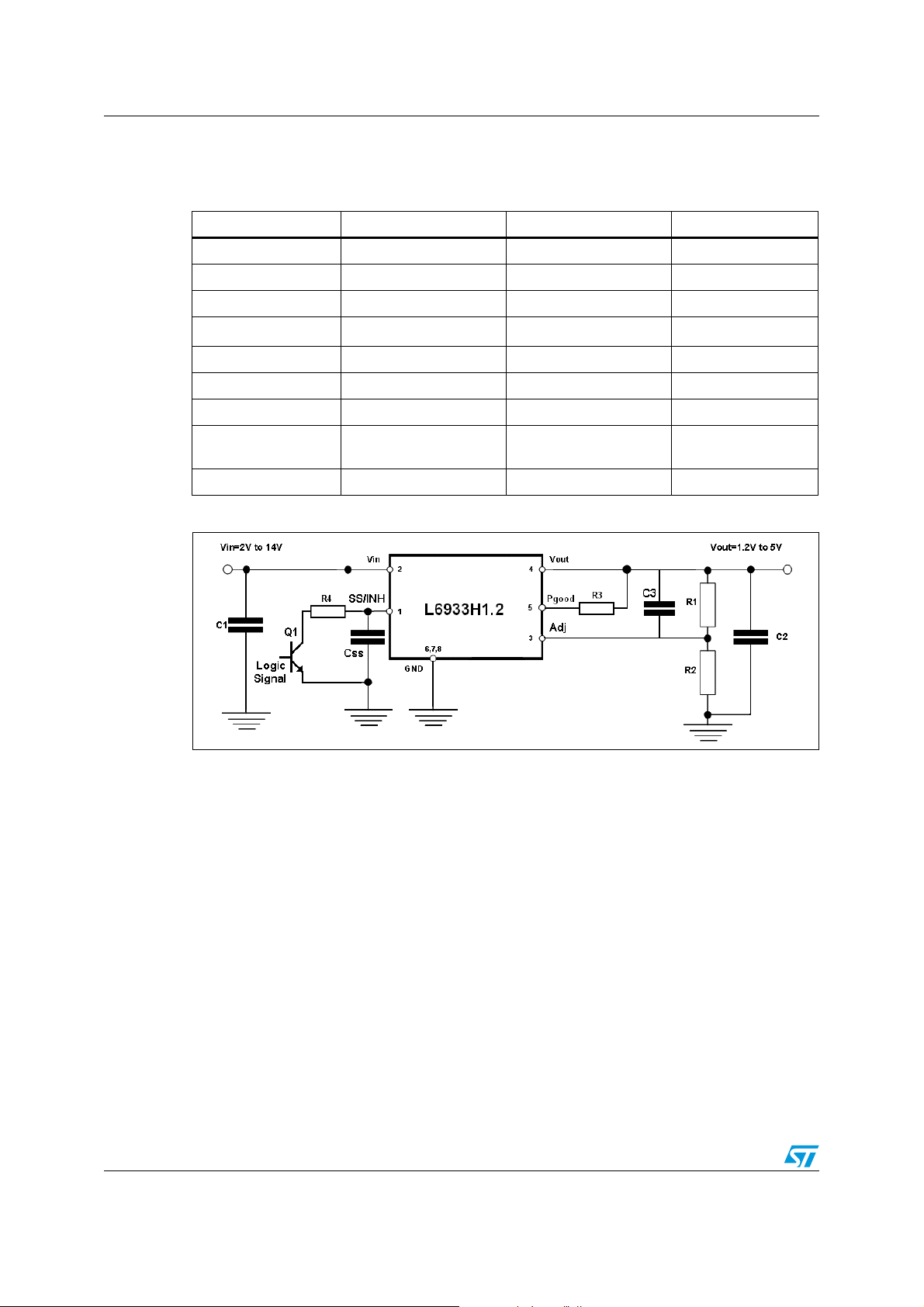
Figure 1. Typical operating circuit
DS(on)
max
L6933H1.2
HSOP8
Description
The L6933H1.2 ultra low drop output linear
regulator operates from 2 V to 14 V and is able to
support output current up to 2 A. Designed with
an internal 50 mΩ N-channel MOSFET, it can be
used for on board DC-DC conversions saving in
real estate, list of components, low noise
generation and power dissipation. L6933H1.2 is
available as adjustable version from 1.2 V to 5 V
with a voltage regulation accuracy of 1 %.
A Soft Start function allows the device to smoothly
increase the Output Voltage at the start-up,
avoiding overshoot. Inhibit function is provided.
The upper current limit is fixed at 2.5 A to control
the current in short circuit condition within ± 8 %.
The current is sensed in the power MOS in order
to limit the power dissipation.
The device is also provided with a thermal shut
down that limits the internal temperature at
150 °C with a histeresys of 20 °C.
Table 1. Device summary
Order codes Package Packaging
L6933H1.2 HSOP8 Tube
L6933H1.2TR HSOP8 Tape and reel
November 2007 Rev 3 1/12
www.st.com
12
Page 2

Contents L6933H1.2
Contents
1 Pin settings . . . . . . . . . . . . . . . . . . . . . . . . . . . . . . . . . . . . . . . . . . . . . . . . 3
1.1 Pin connection . . . . . . . . . . . . . . . . . . . . . . . . . . . . . . . . . . . . . . . . . . . . . . 3
1.2 Pin description . . . . . . . . . . . . . . . . . . . . . . . . . . . . . . . . . . . . . . . . . . . . . . 3
2 Maximum ratings . . . . . . . . . . . . . . . . . . . . . . . . . . . . . . . . . . . . . . . . . . . . 4
2.1 Absolute maximum ratings . . . . . . . . . . . . . . . . . . . . . . . . . . . . . . . . . . . . . 4
2.2 Thermal data . . . . . . . . . . . . . . . . . . . . . . . . . . . . . . . . . . . . . . . . . . . . . . . 4
3 Block diagram . . . . . . . . . . . . . . . . . . . . . . . . . . . . . . . . . . . . . . . . . . . . . . 4
4 Electrical characteristics . . . . . . . . . . . . . . . . . . . . . . . . . . . . . . . . . . . . . 5
5 Typical electrical performance . . . . . . . . . . . . . . . . . . . . . . . . . . . . . . . . . 6
6 Soft-Start . . . . . . . . . . . . . . . . . . . . . . . . . . . . . . . . . . . . . . . . . . . . . . . . . . 6
7 Application information . . . . . . . . . . . . . . . . . . . . . . . . . . . . . . . . . . . . . . 7
7.1 Application circuit . . . . . . . . . . . . . . . . . . . . . . . . . . . . . . . . . . . . . . . . . . . . 7
7.2 Demoboard layout . . . . . . . . . . . . . . . . . . . . . . . . . . . . . . . . . . . . . . . . . . . 7
7.3 Component part list . . . . . . . . . . . . . . . . . . . . . . . . . . . . . . . . . . . . . . . . . . 8
8 Components selection . . . . . . . . . . . . . . . . . . . . . . . . . . . . . . . . . . . . . . . 9
8.1 Input capacitor . . . . . . . . . . . . . . . . . . . . . . . . . . . . . . . . . . . . . . . . . . . . . . 9
8.2 Output capacitor . . . . . . . . . . . . . . . . . . . . . . . . . . . . . . . . . . . . . . . . . . . . . 9
9 Package mechanical data . . . . . . . . . . . . . . . . . . . . . . . . . . . . . . . . . . . . 10
10 Revision history . . . . . . . . . . . . . . . . . . . . . . . . . . . . . . . . . . . . . . . . . . . 11
2/12
Page 3
L6933H1.2 Pin settings
1 Pin settings
1.1 Pin connection
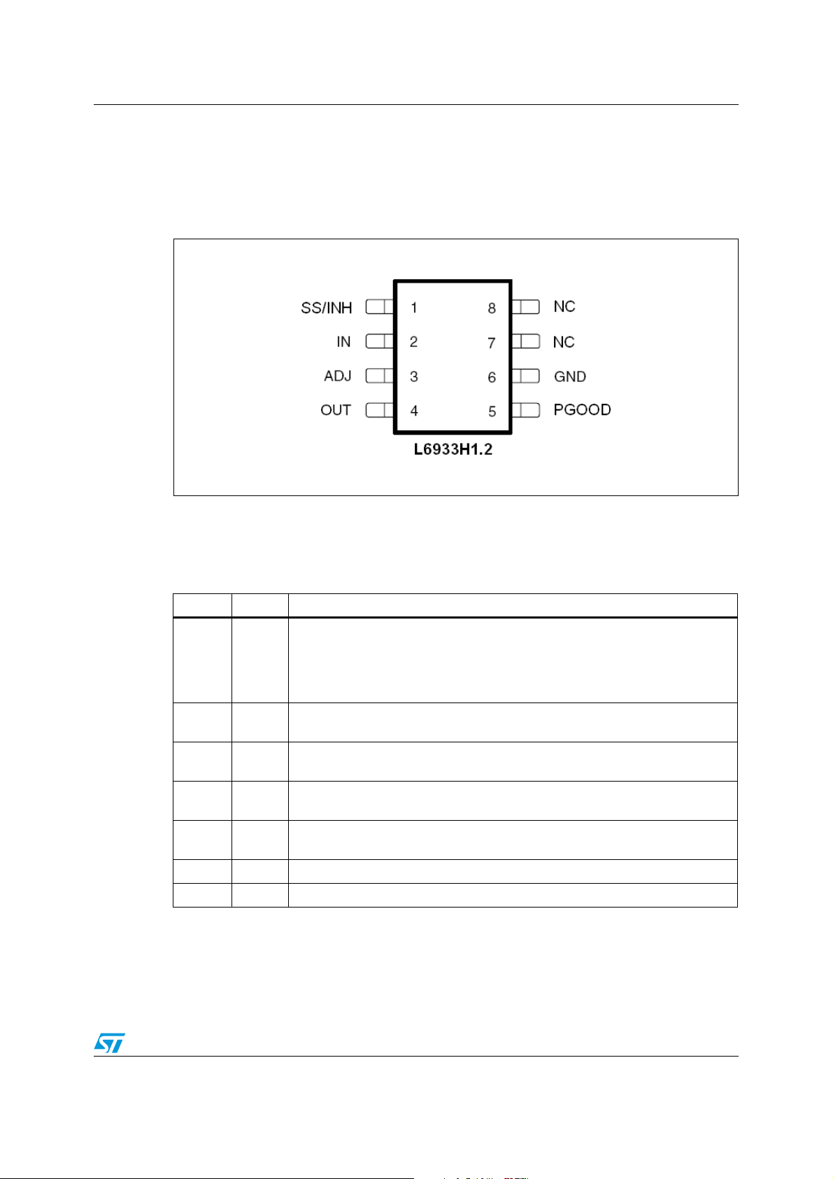
Figure 2. Pin connection (top view)
1.2 Pin description
Table 2. Pin description
Pin N° Name Description
The soft-start time is programmed connecting an external capacitor from this
pin and GND. The internal current generator forces a current of 5 µA through
SS/INH 1
VIN 2
ADJ 3
VOUT 4
PGOOD 5
NC 7, 8 Not connected
GND 6 Ground pins internally connected
the capacitor. In steady state regulation, the voltage at this pin will be about 8 V.
This pin is also used to inhibit the device: when the voltage at this pin is lower
than the 0.5 V, the device is disabled.
Supply voltage. This pin is connected to the drain of the internal N-mos.
Connect this pin to a capacitor larger than 10 µF.
Connecting this pin to a voltage divider it is possible to program the output
voltage between 1.2 V and 5 V.
Regulated output voltage. This pin is connected to the source of the internal Nmos. Connect this pin to a capacitor of 10 µF.
Power good output. The pin is open drain and detects the output voltage. It is
forced low if the output voltage is lower than 90 % the programmed voltage.
3/12
Page 4

Maximum ratings L6933H1.2
2 Maximum ratings
2.1 Absolute maximum ratings
Table 3. Absolute maximum ratings
Symbol Parameter Value Unit
V
IN
2.2 Thermal data
Table 4. Thermal data
Symbol Parameter Value Unit
R
thJA
T
MAX
T
STG
1. Package mounted on board
VIN and PGood 14.5 V
SS/INH, OUT and ADJ -0.3 to (Vin +0.3) V
Maximum thermal resistance junction-ambient
Maximum junction temperature 150 °C
Storage temperature range -65 to 150 °C
34
(1)
°C/W
3 Block diagram
Figure 3. Block diagram
4/12
Page 5
L6933H1.2 Electrical characteristics
4 Electrical characteristics
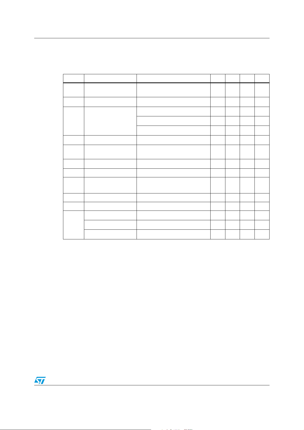
Table 5. Electrical characteristics (TJ = 25 °C, VIN = 5 V unless otherwise specified)
(1)
Symbol Parameter Test condition Min Typ Max Unit
V
r
DS(on)
I
OCC
Operating supply
IN
voltage
V
Output voltage
O
Line regulation
Load regulation
= 0.1 A; VIN = 3.3 V
I
O
V
= 2.5 V ±10 %; IO = 10 mA
IN
V
= 3.3 V ±10 %; IO = 10 mA
IN
V
= 5 V ±10 %; IO = 10 mA
IN
V
= 3.3 V; 0.1 A < IO < 2 A
IN
214V
1.188 1.2 1.212 V
Drain source ON
resistance
Current limiting 2.3 2.5 2.7 A
5mV
5mV
5mV
15 mV
200 mΩ
Iq Quiescent current 0.2 0.4 mA
= 1 A VIN = 5 V,
O
60 75 dB
VINH
Ripple rejection
f = 120 Hz, I
∆VIN = 2 Vpp
INHIBIT input threshold 0.5 V
Iss Soft start current Vss = 0 V -5 uA
P
threshold VO rise 90 %V
GOOD
P
GOOD
1. Specification referred to T from -25 °C to 125 °C.
P
hysteresis 10 %V
GOOD
P
saturation IP
GOOD
= 1 mA 0.2 0.4 V
GOOD
O
O
5/12
Page 6
Typical electrical performance L6933H1.2
5 Typical electrical performance
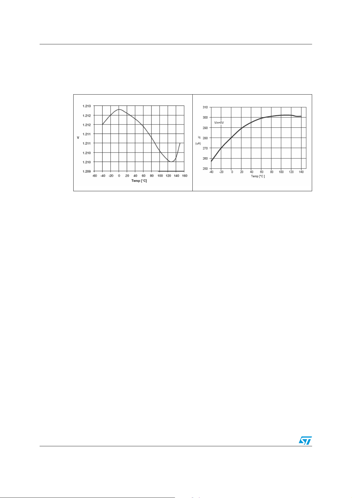
Figure 4. Output voltage vs
junction temperature
Figure 5. Quiescent current vs
junction temperature
6 Soft-Start
When Vin is above the turn-on threshold, the device implements the Soft-Start phase: a
5 µA current is sourced from the SS pin charging the external capacitor. The voltage across
SS capacitor increases until it reaches about 8 V.
The output voltage is in regulation when the SS voltage exceeds V
results:
is below the turn-on threshold, the SS pin is kept shorted to GND.
If V
IN
The SS pin can also be used as ENABLE by shorting the pin to GND through an external
switch: when the voltage at this pin is lower than 0.5 V, the device is disabled.
+ 1 V. The SS time
OUT
C
T
SS
SSVOUT
--------------------------------------------- -=
I
1+()•
SS
6/12
Page 7
L6933H1.2 Application information
7 Application information
7.1 Application circuit
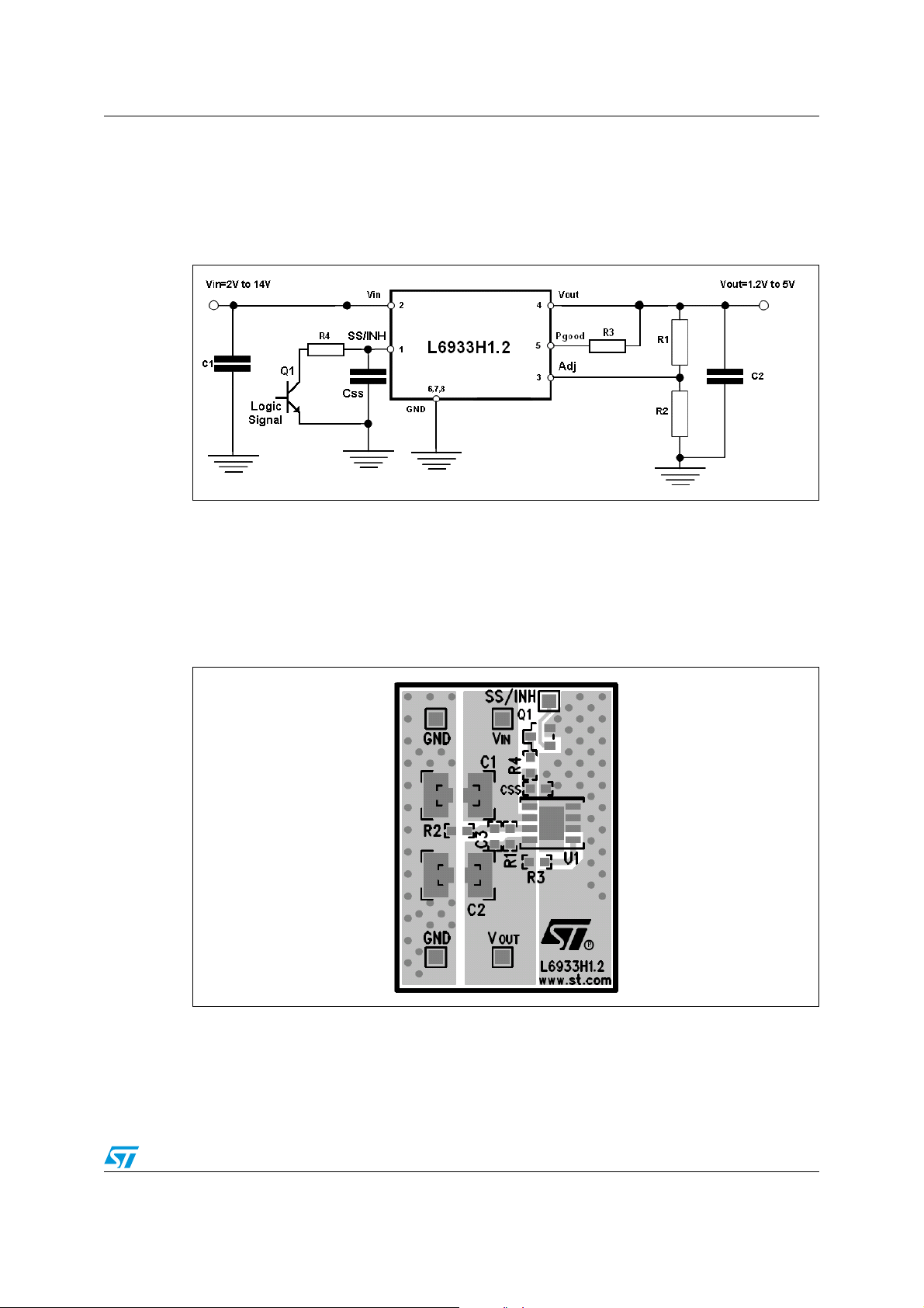
Figure 6. Demoboard application circuit
1.2
V
OUT
------- -
R
+()×=
R
1R2
2
7.2 Demoboard layout
Figure 7. Demoboard layout
Note: SS/INH drives directly the NPN base; its current need to be properly limited.
7/12
Page 8
Application information L6933H1.2
7.3 Component part list
Table 6. Component part list Figure 8
Reference Part number Description Manufacturer
C1 GRM32ER61C226ME20 22 µf, 16 V Murata
C2 GRM32ER61A106KA01 10 µf, 10 V Murata
C3 N.M.
C
SS
R1 0 Ω
R2 N.M.
R3 100 KΩ
Q1 General purpose signal
R4 1 KΩ
Figure 8. Compensation network
10 nF, 16 V
NPN
8/12
Page 9
L6933H1.2 Components selection
8 Components selection
8.1 Input capacitor
The input capacitor value depends on a lot of factors such as load transient requirements,
input source (battery or DC/DC converter) and its distance from the input cap. Usually a
47 µF is enough for any application but a much lower value can be sufficient in many cases.
8.2 Output capacitor
The output capacitor choice depends basically on the load transient requirements.
Tantalum, Special Polymer, POSCAP and aluminum capacitors are good and offer very low
ESR values. Multilayer ceramic caps have the lowest ESR and can be used for particular
applications without affecting the loop stability.
Below a list of some suggested capacitor manufacturers
Table 7. Suggested capacitor
Manufacturer Type Cap value (µF) Rated voltage (V)
Murata Ceramic 1 to 47 4 to 16
Panasonic Ceramic 1 to 47 4 to 16
Tayo Yuden Ceramic 1 to 47 4 to 16
TDK Ceramic 1 to 47 4 to 16
Tokin Ceramic 1 to 47 4 to 16
SANYO Poscap 1 to 47 4 to 16
Panasonic SP 1 to 47 4 to 16
Kemet Tantalum 1 to 47 4 to 16
9/12
Page 10
Package mechanical data L6933H1.2
9 Package mechanical data
In order to meet environmental requirements, ST offers these devices in ECOPACK®
packages. These packages have a Lead-free second level interconnect . The category of
second level interconnect is marked on the package and on the inner box label, in
compliance with JEDEC Standard JESD97. The maximum ratings related to soldering
conditions are also marked on the inner box label. ECOPACK is an ST trademark.
ECOPACK specifications are available at: www.st.com.
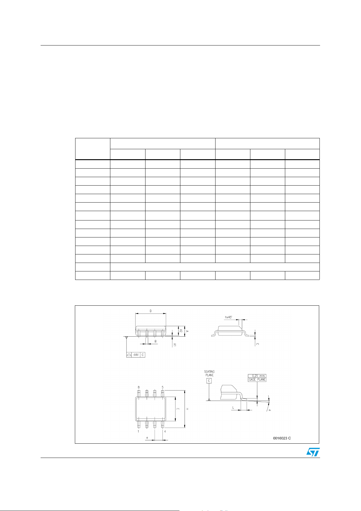
Table 8. SO-8 mechanical data
Dim.
Min Typ Max Min Typ Max
A 1.35 1.75 0.053 0.069
A1 0.10 0.25 0.004 0.010
A2 1.10 1.65 0.043 0.065
B 0.33 0.51 0.013 0.020
C 0.19 0.25 0.007 0.010
(1)
D
4.80 5.00 0.189 0.197
E 3.80 4.00 0.15 0.157
e 1.27 0.050
H 5.80 6.20 0.228 0.244
h 0.25 0.50 0.010 0.020
L 0.40 1.27 0.016 0.050
k 0° (min.), 8° (max.)
ddd 0.10 0.004
1. Dimensions D does not include mold flash, protru-sions or gate burrs. Mold flash, potrusions or gate burrs
shall not exceed 0.15mm (.006inch) in total (both side).
mm. inch
Figure 9. Package dimensions
10/12
Page 11
L6933H1.2 Revision history
10 Revision history
Table 9. Document revision history
Date Revision Changes
21-Mar-2006 1 First release
16-Jul-2007 2 Section 8: Components selection on page 9 updated
22-Nov-2007 3 Updated cover page.
11/12
Page 12

L6933H1.2
Please Read Carefully:
Information in this document is provided solely in connection with ST products. STMicroelectronics NV and its subsidiaries (“ST”) reserve the
right to make changes, corrections, modifications or improvements, to this document, and the products and services described herein at any
time, without notice.
All ST products are sold pursuant to ST’s terms and conditions of sale.
Purchasers are solely responsible for the choice, selection and use of the ST products and services described herein, and ST assumes no
liability whatsoever relating to the choice, selection or use of the ST products and services described herein.
No license, express or implied, by estoppel or otherwise, to any intellectual property rights is granted under this document. If any part of this
document refers to any third party products or services it shall not be deemed a license grant by ST for the use of such third party products
or services, or any intellectual property contained therein or considered as a warranty covering the use in any manner whatsoever of such
third party products or services or any intellectual property contained therein.
UNLESS OTHERWISE SET FORTH IN ST’S TERMS AND CONDITIONS OF SALE ST DISCLAIMS ANY EXPRESS OR IMPLIED
WARRANTY WITH RESPECT TO THE USE AND/OR SALE OF ST PRODUCTS INCLUDING WITHOUT LIMITATION IMPLIED
WARRANTIES OF MERCHANTABILITY, FITNESS FOR A PARTICULAR PURPOSE (AND THEIR EQUIVALENTS UNDER THE LAWS
OF ANY JURISDICTION), OR INFRINGEMENT OF ANY PATENT, COPYRIGHT OR OTHER INTELLECTUAL PROPERTY RIGHT.
UNLESS EXPRESSLY APPROVED IN WRITING BY AN AUTHORIZED ST REPRESENTATIVE, ST PRODUCTS ARE NOT
RECOMMENDED, AUTHORIZED OR WARRANTED FOR USE IN MILITARY, AIR CRAFT, SPACE, LIFE SAVING, OR LIFE SUSTAINING
APPLICATIONS, NOR IN PRODUCTS OR SYSTEMS WHERE FAILURE OR MALFUNCTION MAY RESULT IN PERSONAL INJURY,
DEATH, OR SEVERE PROPERTY OR ENVIRONMENTAL DAMAGE. ST PRODUCTS WHICH ARE NOT SPECIFIED AS "AUTOMOTIVE
GRADE" MAY ONLY BE USED IN AUTOMOTIVE APPLICATIONS AT USER’S OWN RISK.
Resale of ST products with provisions different from the statements and/or technical features set forth in this document shall immediately void
any warranty granted by ST for the ST product or service described herein and shall not create or extend in any manner whatsoever, any
liability of ST.
ST and the ST logo are trademarks or registered trademarks of ST in various countries.
Information in this document supersedes and replaces all information previously supplied.
The ST logo is a registered trademark of STMicroelectronics. All other names are the property of their respective owners.
© 2007 STMicroelectronics - All rights reserved
STMicroelectronics group of companies
Australia - Belgium - Brazil - Canada - China - Czech Republic - Finland - France - Germany - Hong Kong - India - Israel - Italy - Japan -
Malaysia - Malta - Morocco - Singapore - Spain - Sweden - Switzerland - United Kingdom - United States of America
www.st.com
12/12
 Loading...