

High efficiency monolithic synchronous step down regulator
Features
■ 2 V to 5.5 V battery input range
■ High efficiency: up to 95%
■ Internal synchronous switch
■ No external Schottky required
■ Extremely low quiescent current
■ 1 µA max shutdown supply current
■ 800 mA max output current
■ Adjustable output voltage from 0.6 V
■ Low dropout operation: up to 100% duty cycle
■ Selectable low noise/low consumption mode at
light load
■ Power Good signal
■ ± 1% output voltage accuracy
■ Current-mode control
■ 1.4 MHz switching frequency
■ Externally synchronizable from 1 MHz to 2
MHz
■ OVP
■ Short-circuit protection
Applications
■ Battery-powered equipment
■ Portable instruments
■ Cellular phones
■ PDAs and hand held terminals
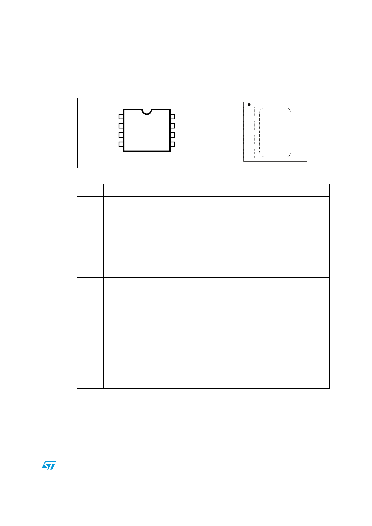
Figure 1. Application test circuit
VIN= 2 to 5.5 V
C1
10µF
6.3V
V
RUN
SYNC
CC
6
1
7
R1
10k
24
C3
220pF
L6928
MSOP8
■ DSC
■ GPS
Description
The device is DC-DC monolithic regulator
specifically designed to provide extremely high
efficiency. L6928 supply voltage can be as low as
2 V allowing its use in single Li-Ion cell supplied
applications. Output voltage can be selected by
an external divider down to 0.6 V. Duty cycle can
saturate to 100% allowing low dropout operation.
The device is based on a 1.4 MHz fixed
frequency, current mode architecture. Low
consumption mode operation can be selected at
light load conditions, allowing switching losses to
be reduced. L6928 is externally synchronizable
with a clock which makes it useful in noise
sensitive applications. Other features like Power
Good, overvoltage protection, short-circuit
protection and thermal shutdown (150 °C) are
also present.
L 4.7 µH
LX
5
8
3
GNDCOMP
PGOOD
VFB
R3
500k
R2
200k
R1
100k
V
C2
10µF
6.3V
IN
= 1.8 V
AM10473v1
VFQFPN8
(3x3x1.0 mm)
December 2011 Doc ID 11051 Rev 7 1/16
www.st.com
16

Contents L6928
Contents
1 Pin settings . . . . . . . . . . . . . . . . . . . . . . . . . . . . . . . . . . . . . . . . . . . . . . . . 3
2 Maximum ratings . . . . . . . . . . . . . . . . . . . . . . . . . . . . . . . . . . . . . . . . . . . . 4
3 Electrical characteristics . . . . . . . . . . . . . . . . . . . . . . . . . . . . . . . . . . . . . 5
4 Operation description . . . . . . . . . . . . . . . . . . . . . . . . . . . . . . . . . . . . . . . . 7
4.1 Modes of operation . . . . . . . . . . . . . . . . . . . . . . . . . . . . . . . . . . . . . . . . . . . 7
4.1.1 Low consumption mode . . . . . . . . . . . . . . . . . . . . . . . . . . . . . . . . . . . . . . 8
4.1.2 Low noise mode . . . . . . . . . . . . . . . . . . . . . . . . . . . . . . . . . . . . . . . . . . . . 8
4.1.3 Synchronization . . . . . . . . . . . . . . . . . . . . . . . . . . . . . . . . . . . . . . . . . . . . 8
4.2 Short circuit protection . . . . . . . . . . . . . . . . . . . . . . . . . . . . . . . . . . . . . . . . 8
4.3 Slope compensation . . . . . . . . . . . . . . . . . . . . . . . . . . . . . . . . . . . . . . . . . . 9
4.4 Loop stability . . . . . . . . . . . . . . . . . . . . . . . . . . . . . . . . . . . . . . . . . . . . . . . 9
5 Additional features and protections . . . . . . . . . . . . . . . . . . . . . . . . . . . 10
5.1 DROPOUT operation . . . . . . . . . . . . . . . . . . . . . . . . . . . . . . . . . . . . . . . . 10
5.2 PGOOD (Power Good output) . . . . . . . . . . . . . . . . . . . . . . . . . . . . . . . . . 10
5.3 Adjustable output voltage . . . . . . . . . . . . . . . . . . . . . . . . . . . . . . . . . . . . . 10
5.4 OVP (Overvoltage protection) . . . . . . . . . . . . . . . . . . . . . . . . . . . . . . . . . 10
5.5 Thermal shutdown . . . . . . . . . . . . . . . . . . . . . . . . . . . . . . . . . . . . . . . . . . 10
6 Package mechanical data . . . . . . . . . . . . . . . . . . . . . . . . . . . . . . . . . . . . 11
7 Order codes . . . . . . . . . . . . . . . . . . . . . . . . . . . . . . . . . . . . . . . . . . . . . . . 14
8 Revision history . . . . . . . . . . . . . . . . . . . . . . . . . . . . . . . . . . . . . . . . . . . 15
2/16 Doc ID 11051 Rev 7
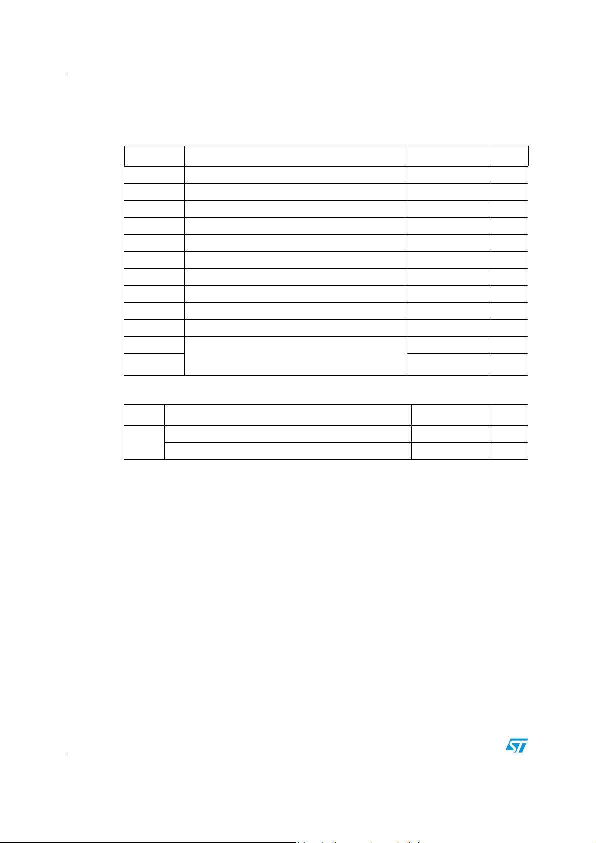
L6928 Pin settings
1 Pin settings
Figure 2. Pin connection (top view)
RUN
COMP
VFB
GND
1
2
3
4LX
D01IN1239AMOD
PGOOD8
SYNC
7
V
6
CC
5
Table 1. Pin description
Pin n° Name Description
1RUN
2COMP
3 VFB
4 GND Ground.
5LX
6V
7 SYNC
8 PGOOD
Shutdown input. When connected to a low level (lower than 0.4 V) the device
stops working. When high (higher than 1.3 V) the device is enabled.
Error amplifier output. A compensation network has to be connected to this pin.
Usually a 220 pF capacitor is enough to guarantee the loop stability.
Error amplifier inverting input. The output voltage can be adjusted from 0.6 V up
to the input voltage by connecting this pin to an external resistor divider.
Switch output node. This pin is internally connected to the drain of the internal
switches.
Input voltage. The start up input voltage is 2.2 V (typ) while the operating input
voltage range is from 2 V to 5.5 V. An internal UVLO circuit realizes a 100 mV
CC
(typ.) hysteresis.
Operating mode selector input. When high (higher than 1.3 V) the low
consumption mode is selected. When low (lower than 0.5 V) the low noise mode
is selected. If connected with an appropriate external synchronization signal
(from 500 kHz up to 1.4 MHz) the internal synchronization circuit is activated
and the device works at the same switching frequency.
Power good comparator output. It is an open drain output. A pull-up resistor
should be connected between PGOOD and V
requirements). The pin is forced low when the output voltage is lower than 90%
of the regulated output voltage and goes high when the output voltage is greater
than 90% of the regulated output voltage. If not used the pin can be left floating.
RUN
COMP
VFB
GND
1
2
E-pad
3
4
AM10471v1
(or VCC depending on the
OUT
8
7
6
5
PGOOD
SYNC
V
CC
LX
- E-Pad To be connected to GND plane for optimal thermal performance.
Doc ID 11051 Rev 7 3/16
Maximum ratings L6928
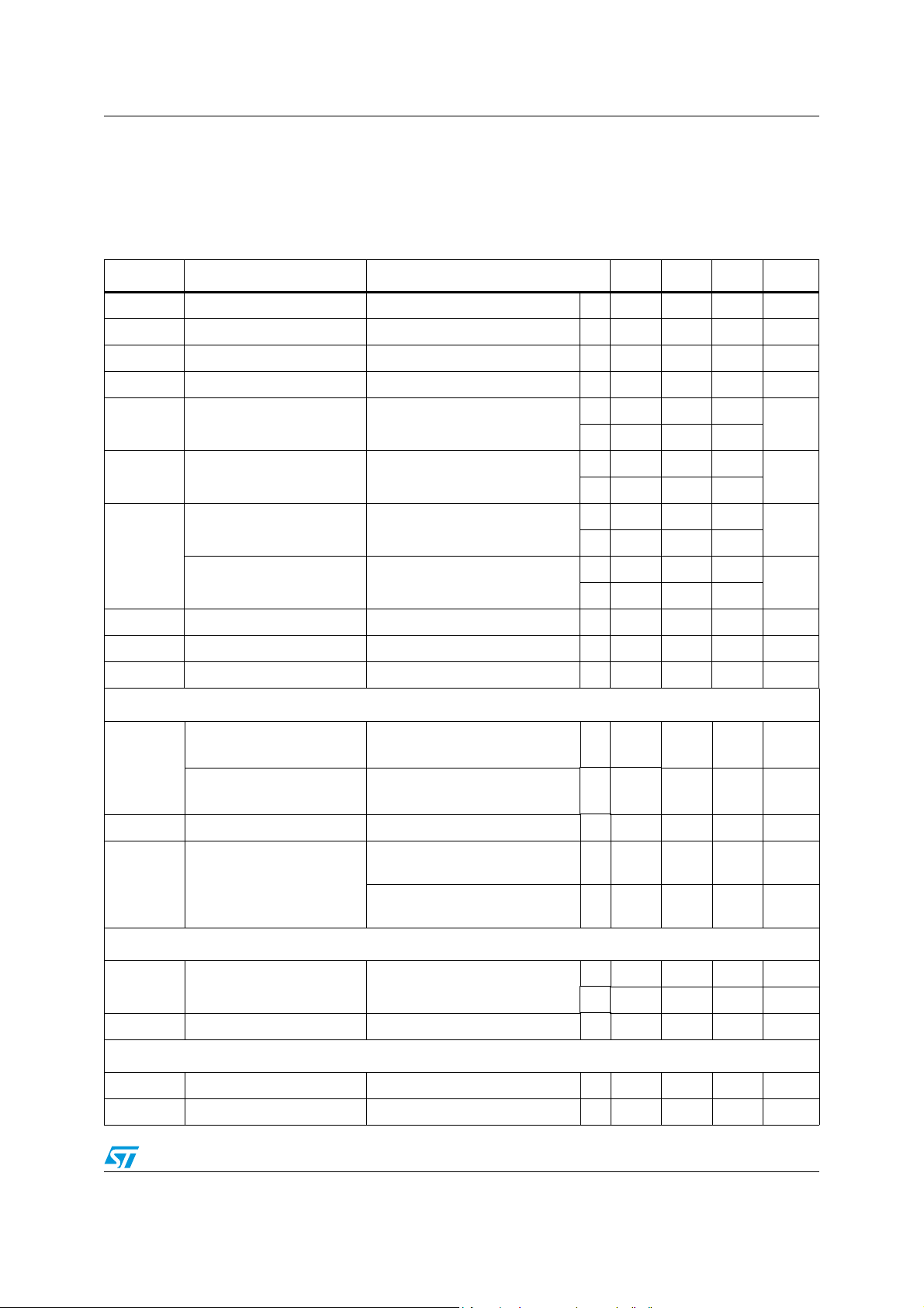
2 Maximum ratings
Table 2. Absolute maximum ratings
Symbol Parameter Value Unit
V
6
V
5
V
1
V
3
V
2
V
8
V
7
P
TOT
T
J
T
STG
LX pin Maximum withstanding voltage range test condition:
Input voltage -0.3 to 6 V
Output switching voltage -1 to V
Shutdown -0.3 to V
Feedback voltage -0.3 to V
Error amplifier output voltage -0.3 to V
PGOOD -0.3 to V
Synchronization mode selector -0.3 to V
CC
CC
CC
CC
CC
CC
Power dissipation at TA = 70 °C0.45W
Junction operating temperature range -40 to 150 °C
Storage temperature range -65 to 150 °C
±1000 V
CDF-AEC-Q100-002- “Human body model”
Other pins ±2000 V
acceptance criteria: “normal performance’
Table 3. Thermal data
Symbol Parameter Value Unit
R
Maximum thermal resistance junction-ambient for MSOP8 180 °C/W
thJA
Maximum thermal resistance junction-ambient for VFQFPN8 56 °C/W
V
V
V
V
V
V
4/16 Doc ID 11051 Rev 7
L6928 Electrical characteristics
3 Electrical characteristics
TJ = 25 °C, VIN = 3.6 V unless otherwise specified.
Table 4. Electrical characteristics
.
Symbol Parameter Test condition Min. Typ. Max. Unit
V
V
cc ON
V
cc OFF
V
cc hys
R
R
Operating input voltage After turn on
cc
Turn On threshold 2.2 V
Turn Off threshold 2 V
Hysteresis 100 mV
High side R
p
n
Low side R
ON
ON
Peak current limit Vcc = 3.6 V
I
lim
Valley current limit V
V
f
OUT
f
osc
sync
Output voltage range V
Oscillator frequency 1.4 MHz
Sync mode clock
(2)
DC characteristics
(1)
V
cc
V
cc
cc
= 3.6 V, I
= 3.6 V, I
= 3.6 V
=100 mA
lx
=100 mA
lx
(1)
25.5V
240 300
(1)
400
mΩ
215 300
(1)
400
mΩ
11.21.5
(1)
0.85 1.65
A
11.41.7
(1)
0.9 1.85
fb
V
CC
A
V
12MHz
Quiescent current (low
noise mode)
I
q
Quiescent current (low
consumption mode)
I
sh
I
lx
Shutdown current RUN to GND, V
LX leakage current
Error amplifier characteristics
V
I
fb
Voltage feedback
fb
Feedback input current
Run
V
V
run_H
run_L
RUN threshold high 1.3 V
RUN threshold low 0.4 V
(2)
= 0 V, no load,
V
sync
> 0.6 V
V
FB
= VCC, no load,
V
sync
> 0.6 V
V
FB
RUN to GND, V
V
= 5.5 V
CC
RUN to GND, V
= 5.5 V
V
CC
(1)
= 5.5 V 0.2 µA
CC
= 5.5 V,
LX
= 0 V,
LX
230µA
25 50 µA
1µA
1µA
0.593 0.600 0.607 V
(1)
0.590 0.600 0.610 V
(2)
VFB = 0.6 V 25 nA
Doc ID 11051 Rev 7 5/16

Electrical characteristics L6928
Table 4. Electrical characteristics (continued)
(1)
Symbol Parameter Test condition Min. Typ. Max. Unit
I
run
RUN input current
(2)
25 nA
SYNC/MODE function
V
sync_H
V
sync_L
Sync mode threshold high 1.3 V
Sync mode threshold low 0.5 V
PGOOD section
V
PGOOD
ΔV
PGOOD
V
Pgood(low)
I
LK-PGOOD
Power Good Threshold V
Power Good Hysteresis V
OUT
OUT
= V
= V
fb
fb
90 %V
4%V
Power Good Low Voltage Run to GND 0.4 V
Power Good Leakage
Current
(2)
V
PGOOD
= 3.6 V 50 nA
Protections
HOVP Hard overvoltage threshold V
1. Specification referred to TJ from -40°C to +125°C. Specification over the -40 to +125°C TJ temperature range are assured
by design, characterization and statistical correlation.
2. Guaranteed by design.
OUT
= V
fb
10 %V
OUT
OUT
OUT
6/16 Doc ID 11051 Rev 7

L6928 Operation description
4 Operation description
The main loop uses slope compensated PWM current mode architecture. Each cycle the
high side MOSFET is turned on, triggered by the oscillator, so that the current flowing
through it (the same as the inductor current) increases. When this current reaches the
threshold (set by the output of the error amplifier E/A), the peak current limit comparator
PEAK_CL turns off the high side MOSFET and turns on the low side one until the next clock
cycle begins or the current flowing through it goes down to zero (ZERO CROSSING
comparator). The peak inductor current required to trigger PEAK_CL depends on the slope
compensation signal and on the output of the error amplifier.
In particular, the error amplifier output depends on the VFB pin voltage. When the output
current increases, the output capacitor is discharged and so the VFB pin decreases. This
produces increase of the error amplifier output, so allowing a higher value for the peak
inductor current. For the same reason, when due to a load transient the output current
decreases, the error amplifier output goes low, so reducing the peak inductor current to
meet the new load requirements.
The slope compensation signal allows the loop stability also in high duty cycle conditions
(see related section).
Figure 3. Device block diagram
RUN
SYNC
SYNC
RUN
VCC
VCC
LOW
LOW
NOISE/
COMP
COMP
FB
FB
P
P
GOOD
GOOD
CONSUMPTION
CONSUMPTION
V
V
REF
REF
0.6V
0.6V
V
V
REF
REF
0.9V
0.9V
NOISE/
E/A
E/A
P
P
GOOD
GOOD
OVP
OVP
4.1 Modes of operation
Depending on the SYNC pin value the device can operate in low consumption or low noise
mode. If the SYNC pin is high (higher than 1.3 V) the low consumption mode is selected
while the low noise mode is selected if the SYNC pin is low (lower than 0.5 V).
OSCILLATOR
OSCILLATOR
LOOP
LOOP
CONTROL
CONTROL
ZERO
ZERO
CROSSING
CROSSING
PEAK
PEAK
CL
CL
GND
GND
VAL LE Y
VAL LE Y
CL
CL
GND
GND
Vcc
Vcc
SENS E
SENS E
P
P
MOS
MOS
SLOPE
SLOPE
SENS E
SENS E
N
N
MOS
MOS
GND
GND
DRIVER
DRIVER
Vcc
Vcc
GND
GND
POWER
POWER
P
P
MOS
MOS
POWER
POWER
N
N
MOS
MOS
LX
LX
Doc ID 11051 Rev 7 7/16

Operation description L6928
4.1.1 Low consumption mode
In this mode of operation, at light load, the device operates discontinuously based on the
COMP pin voltage, in order to keep the efficiency very high also in these conditions. While
the device is not switching the load discharges the output capacitor and the output voltage
goes down. When the feedback voltage goes lower than the internal reference, the COMP
pin voltage increases and when an internal threshold is reached, the device starts to switch.
In these conditions the peak current limit is set approximately in the range of 200 mA - 400
mA, depending on the slope compensation (see related section).
Once the device starts to switch the output capacitor is recharged. The feedback pin
increases and, when it reaches a value slightly higher than the reference voltage, the output
of the error amplifier goes down until a clamp is activated. At this point, the device stops to
switch. In this phase, most of the internal circuitries are off, so reducing the device
consumption down to a typical value of 25 µA.
4.1.2 Low noise mode
If for noise reasons, the very low frequencies of the low consumption mode are undesirable,
the low noise mode can be selected. In low noise mode, the efficiency is a little bit lower
compared with the low consumption mode in very light load conditions but for medium-high
load currents the efficiency values are very similar.
Basically, the device switches with its internal free running frequency of 1.4 MHz. Obviously,
in very light load conditions, the device could skip some cycles in order to keep the output
voltage in regulation.
4.1.3 Synchronization
The device can also be synchronized with an external signal from 1 MHz up to 2 MHz.
In this case the low noise mode is automatically selected. The device will eventually skip
some cycles in very light load conditions. The internal synchronization circuit is inhibited in
short-circuit and overvoltage conditions in order to keep the protections effective (see
relative sections).
4.2 Short circuit protection
During the device operation, the inductor current increases during the high side turn ON
phase and decrease during the high side turn off phase based on the following equations:
Equation 1
ΔI
Equation 2
ON
VINV
–()
----------------------------------
OUT
L
⋅=
T
ON
V
()
OUT
OFF
-------------------
L
ΔI
In strong overcurrent or short-circuit conditions the V
case ΔI
8/16 Doc ID 11051 Rev 7
increases and ΔI
ON
decreases. When the inductor peak current reaches the
OFF
⋅=
T
OFF
can be very close to zero. In this
OUT

L6928 Operation description
current limit, the high side MOSFET turns off and so the TON is reduced down to the
minimum value (250 ns typ.) in order to reduce as much as possible ΔI
Anyway, if V
because during the T
is low enough it can be that the inductor peak current further increases
OUT
the current decays very slowly.
OFF
ON
.
Due to this reason a second protection that fixes the maximum inductor valley current has
been introduced. This protection doesn't allow the high side MOSFET to turn on if the
current flowing through the inductor is higher that a specified threshold (valley current limit).
Basically the T
is increased as much as required to bring the inductor current down to
OFF
this threshold. So, the maximum peak current in worst case conditions will be:
Equation 3
V
IN
-------- -
I
PEAKIVALLEY
T
⋅+=
ON_MIN
L
Where I
is the valley current limit (1.4 A typ.) and T
PEAK
high side MOSFET.
4.3 Slope compensation
In current mode architectures, when the duty cycle of the application is higher than
approximately 50%, a pulse-by-pulse instability (the so called sub harmonic oscillation) can
occur. To allow loop stability also in these conditions a slope compensation is present. This
is realized by reducing the current flowing through the inductor necessary to trigger the
COMP comparator (with a fixed value for the COMP pin voltage). With a given duty cycle
higher than 50%, the stability problem is particularly present with an higher input voltage
(due to the increased current ripple across the inductor), so the slope compensation effect
increases as the input voltage increases. From an application point of view, the final effect is
that the peak current limit depends both on the duty cycle (if higher than approximately 40%)
and on the input voltage.
4.4 Loop stability
Since the device is realized with a current mode architecture, the loop stability is usually not
a big issue. For most of the application a 220 pF connected between the COMP pin and
ground is enough to guarantee the stability. In case very low ESR capacitors are used for
the output filter, such as multilayer ceramic capacitors, the zero introduced by the capacitor
itself can shift at very high frequency and the transient loop response could be affected.
Adding a series resistor to the 220 pF capacitor can solve this problem.
ON_MIN
is the minimum TON of the
The right value for the resistor (in the range of 50 K) can be determined by checking the load
transient response of the device. Basically, the output voltage has to be checked at the
scope after the load steps required by the application. In case of stability problems, the
output voltage could oscillates before to reach the regulated value after a load step.
Doc ID 11051 Rev 7 9/16

Additional features and protections L6928
5 Additional features and protections
5.1 DROPOUT operation
The Li-Ion battery voltage ranges from approximately 3 V and 4.1 V - 4.2 V (depending on
the anode material). In case the regulated output voltage is from 2.5 V and 3.3 V, it can be
that, close to the end of the battery life, the battery voltage goes down to the regulated one.
In this case the device stops to switch, working at 100% of duty cycle, so minimizing the
dropout voltage and the device losses.
5.2 PGOOD (Power Good output)
A power good output signal is available. The VFB pin is internally connected to a comparator
with a threshold set at 90% of the of reference voltage (0.6 V). Since the output voltage is
connected to the V
regulated value, the V
The internal comparator is triggered and the PGOOD pin is pulled down.
The pin is an open drain output and so, a pull up resistor should be connected to him.
If the feature is not required, the pin can be left floating.
pin by a resistor divider, when the output voltage goes lower than the
FB
pin voltage goes lower than 90% of the internal reference value.
FB
5.3 Adjustable output voltage
The output voltage can be adjusted by an external resistor divider from a minimum value of
0.6 V up to the input voltage. The output voltage value is given by:
Equation 4
V
OUT
5.4 OVP (Overvoltage protection)
The device has an internal overvoltage protection circuit to protect the load.
If the voltage at the feedback pin goes higher than an internal threshold set 10% (typ) higher
than the reference voltage, the low side power MOSFET is turned on until the feedback
voltage goes lower than the reference one.
During the overvoltage circuit intervention, the zero crossing comparator is disabled so that
the device is also able to sink current.
5.5 Thermal shutdown
⎛⎞
0.6 1
⋅=
⎝⎠
R
2
------ -+
R
1
The device has also a thermal shutdown protection activated when the junction temperature
reaches 150 °C. In this case both the high side MOSFET and the low side one are turned
off. Once the junction temperature goes back lower than 95 °C, the device restarts the
normal operation.
10/16 Doc ID 11051 Rev 7

L6928 Package mechanical data
6 Package mechanical data
In order to meet environmental requirements, ST offers these devices in different grades of
ECOPACK
specifications, grade definitions and product status are available at: www.st.com.
ECOPACK
®
packages, depending on their level of environmental compliance. ECOPACK®
®
is an ST trademark.
Table 5. MSOP8 mechanical data
mm.
Dim.
Min. Typ. Max.
A 1.10
A1 0 0.15
A2 0.75 0.85 0.95
b 0.22 0.40
c 0.08 0.23
(1)
D
E 4.65 4.90 5.15
(1)
E1
e0.65
L 0.40 0.60 0.80
L1 0.95
2.80 3.00 3.20
2.80 3.00 3.10
L2 0.25
k0 8
ccc 0.10
1. Dimension “D” and “E1” does not include mold flash or protrusions. Mold flash or protrusions shall not
exceed 0.15 mm per side.
Doc ID 11051 Rev 7 11/16

Package mechanical data L6928
Figure 4. MSOP8 package dimensions
12/16 Doc ID 11051 Rev 7
7113595_B

L6928 Package mechanical data
mm inch
DIM.
MIN. TYP. MAX. MIN. TYP. MAX.
A 0.80 0.90 1.00 0.0315 0.0354 0.0394
A1 0.02 0.05 0.0008 0.0020
A2 0.70 0.0276
A3 0.20 0.0079
b0.180.23 0.30 0.0071 0.0091 0.0118
D 3.00 0.1181
D2 2.23 2.38 2.48 0.0878 0.09370.0976
E 3.00 0.1181
E2 1.49 1.64 1.74 0.0587 0.0646 0.0685
e 0.50 0.0197
L0.30 0.40 0.50 0.0118 0.0157 0.0197
ddd 0.08 0.0031
OUTLINE AND
MECHANICAL DATA
VFQFPN8 (3x3x1.0 8mm)
Very thin Fine pitch Quad Packages No lead
7426334 B
Doc ID 11051 Rev 7 13/16

Order codes L6928
7 Order codes
Table 1. Order codes
Order codes Package Packaging
L6928D MSOP8 Tube
L6928D013TR MSOP8 Tape and reel
L6928Q1 VFQFPN8 Tube
L6928Q1TR VFQFPN8 Tape and reel
14/16 Doc ID 11051 Rev 7

L6928 Revision history
8 Revision history
Table 6. Document revision history
Date Revision Changes
Oct-2004 1 First Issue.
Feb-2005 2 Changed from product preview to final datasheet.
Nov-2005 3
27-Oct-2006 4 Added R
22-Aug-2007 5 Updated Table 1: Order codes on page 14.
11-Apr-2011 6
Updated Table 5. Electrical characteristics.
Added VFQFPN8 package and new part numbers.
for VFQFPN8 in Table 3.
thJA
Updated MSOP8 package mechanical data Table 5 on page 11 and
Figure 4 on page 12.
20-Dec-2011 7
Updated Figure 1 on page 1.
Added pin connection Figure 2 on page 3.
Doc ID 11051 Rev 7 15/16

L6928
Please Read Carefully:
Information in this document is provided solely in connection with ST products. STMicroelectronics NV and its subsidiaries (“ST”) reserve the
right to make changes, corrections, modifications or improvements, to this document, and the products and services described herein at any
time, without notice.
All ST products are sold pursuant to ST’s terms and conditions of sale.
Purchasers are solely responsible for the choice, selection and use of the ST products and services described herein, and ST assumes no
liability whatsoever relating to the choice, selection or use of the ST products and services described herein.
No license, express or implied, by estoppel or otherwise, to any intellectual property rights is granted under this document. If any part of this
document refers to any third party products or services it shall not be deemed a license grant by ST for the use of such third party products
or services, or any intellectual property contained therein or considered as a warranty covering the use in any manner whatsoever of such
third party products or services or any intellectual property contained therein.
UNLESS OTHERWISE SET FORTH IN ST’S TERMS AND CONDITIONS OF SALE ST DISCLAIMS ANY EXPRESS OR IMPLIED
WARRANTY WITH RESPECT TO THE USE AND/OR SALE OF ST PRODUCTS INCLUDING WITHOUT LIMITATION IMPLIED
WARRANTIES OF MERCHANTABILITY, FITNESS FOR A PARTICULAR PURPOSE (AND THEIR EQUIVALENTS UNDER THE LAWS
OF ANY JURISDICTION), OR INFRINGEMENT OF ANY PATENT, COPYRIGHT OR OTHER INTELLECTUAL PROPERTY RIGHT.
UNLESS EXPRESSLY APPROVED IN WRITING BY TWO AUTHORIZED ST REPRESENTATIVES, ST PRODUCTS ARE NOT
RECOMMENDED, AUTHORIZED OR WARRANTED FOR USE IN MILITARY, AIR CRAFT, SPACE, LIFE SAVING, OR LIFE SUSTAINING
APPLICATIONS, NOR IN PRODUCTS OR SYSTEMS WHERE FAILURE OR MALFUNCTION MAY RESULT IN PERSONAL INJURY,
DEATH, OR SEVERE PROPERTY OR ENVIRONMENTAL DAMAGE. ST PRODUCTS WHICH ARE NOT SPECIFIED AS "AUTOMOTIVE
GRADE" MAY ONLY BE USED IN AUTOMOTIVE APPLICATIONS AT USER’S OWN RISK.
Resale of ST products with provisions different from the statements and/or technical features set forth in this document shall immediately void
any warranty granted by ST for the ST product or service described herein and shall not create or extend in any manner whatsoever, any
liability of ST.
ST and the ST logo are trademarks or registered trademarks of ST in various countries.
Information in this document supersedes and replaces all information previously supplied.
The ST logo is a registered trademark of STMicroelectronics. All other names are the property of their respective owners.
© 2011 STMicroelectronics - All rights reserved
STMicroelectronics group of companies
Australia - Belgium - Brazil - Canada - China - Czech Republic - Finland - France - Germany - Hong Kong - India - Israel - Italy - Japan -
Malaysia - Malta - Morocco - Philippines - Singapore - Spain - Sweden - Switzerland - United Kingdom - United States of America
www.st.com
16/16 Doc ID 11051 Rev 7
 Loading...