


Highly integrated ballast controller for TL and CFL
Features
■ Half bridge circuit able to drive both BJT and
MOSFET transistors
■ Very accurate oscillator precision in wide
operating temperature range
■ BJTs' storage time compensation
■ Preheated start and instant start
■ Hard switching protection
■ Overcurrent / voltage protection
■ Choke saturation control
■ End-of-life protection
■ Programmable without capacitors
L6520
L6521
SO8
Applications
■ Electronic ballasts (TL, Industrial CFL)
■ Integrated CFLs
Table 1. Device summary
Order codes Package Packaging
L6520
Tube
Figure 1. Block diagram
3:0BGHW
9
9
(2/
)35(
9
9FF
X$
L6520TR Tape and reel
SO8
L6521 Tube
L6521TR Tape and reel
9&&
9FF
6WDUW8S 89/2
9
,1
9
$'&
9
,QWHUQDO9
/2*,&
9
9
5HJ
&25(
&&&%ORFN
9FF
7[0 7[/7[+
7KUHVKROG08;
+6'
/6'
+%&6
*1'
March 2011 Doc ID 16998 Rev 3 1/19
www.st.com
19

Contents L6520, L6521
Contents
1 Description . . . . . . . . . . . . . . . . . . . . . . . . . . . . . . . . . . . . . . . . . . . . . . . . . 3
2 Pin connection . . . . . . . . . . . . . . . . . . . . . . . . . . . . . . . . . . . . . . . . . . . . . . 4
3 Maximum ratings . . . . . . . . . . . . . . . . . . . . . . . . . . . . . . . . . . . . . . . . . . . . 5
4 Electrical characteristics . . . . . . . . . . . . . . . . . . . . . . . . . . . . . . . . . . . . . 6
5 Functions description . . . . . . . . . . . . . . . . . . . . . . . . . . . . . . . . . . . . . . . . 9
5.1 Start-up . . . . . . . . . . . . . . . . . . . . . . . . . . . . . . . . . . . . . . . . . . . . . . . . . . . 9
5.2 Preheating and instant start . . . . . . . . . . . . . . . . . . . . . . . . . . . . . . . . . . . . 9
5.3 Ignition . . . . . . . . . . . . . . . . . . . . . . . . . . . . . . . . . . . . . . . . . . . . . . . . . . . 10
5.4 Run mode . . . . . . . . . . . . . . . . . . . . . . . . . . . . . . . . . . . . . . . . . . . . . . . . . 10
5.5 Storage time compensation network . . . . . . . . . . . . . . . . . . . . . . . . . . . . 10
5.6 Current control circuit (CCC) . . . . . . . . . . . . . . . . . . . . . . . . . . . . . . . . . . 11
5.6.1 Hard switching protection (HSP) . . . . . . . . . . . . . . . . . . . . . . . . . . . . . . 11
5.6.2 Overcurrent protection (OCPH) during ignition mode . . . . . . . . . . . . . . 11
5.6.3 Overcurrent protection (OCPL) during run mode . . . . . . . . . . . . . . . . . . 11
5.6.4 Choke saturation control (CSC) during ignition and run mode . . . . . . . 12
5.7 End of life (EOL) . . . . . . . . . . . . . . . . . . . . . . . . . . . . . . . . . . . . . . . . . . . . 12
5.8 Summary of protections . . . . . . . . . . . . . . . . . . . . . . . . . . . . . . . . . . . . . . 13
6 Typical electrical characteristics . . . . . . . . . . . . . . . . . . . . . . . . . . . . . . 14
7 Application examples . . . . . . . . . . . . . . . . . . . . . . . . . . . . . . . . . . . . . . . 15
8 Package mechanical data . . . . . . . . . . . . . . . . . . . . . . . . . . . . . . . . . . . . 16
9 Revision history . . . . . . . . . . . . . . . . . . . . . . . . . . . . . . . . . . . . . . . . . . . 18
2/19 Doc ID 16998 Rev 3

L6520, L6521 Description
1 Description
The L6520/1 is the first highly integrated ballast controller in the market able to drive both
BJTs and MOSFETs, providing all the necessary protections to ensure the maximum
reliability of the application in compliance with major safety and power consumption
regulations.
By adopting BJTs switches in the application, the IC allows to replace more expensive
MOSFETs, strongly reducing the system cost without compromises.
The IC represents also the best and cost effective solution to replace self oscillating
solutions when the key requirement is the reliability of the ballast. The benefits are an
increased MTBF and a reduction of the costs due to the return from the field.
The higher level of flexibility and integration provided allows the possibility to quickly design
ballast with any kind of lamp topology/size/power, without limitations. Depending on the
power of the lamp, the IC can work without PFC, with passive PFC or with active PFC. In the
latter case the L6562A from STMicroelectronics is the suggested IC for the most cost
effective solution.
The IC is fully programmable using only resistors and offers over current protections, choke
saturation control and hard switching protection thanks to a sophisticated current control
circuit (CCC). In ignition, the CCC limits both the maximum lamp voltage in case of old or
broken lamp, and also the lamp current in case of inductor saturation.
When the IC is driving bipolar transistors, a variable dead time ensures the correct base
discharge time avoiding cross conduction phenomena. Moreover, the IC prevents the failure
due to the lamp's end of life (EOL).
Doc ID 16998 Rev 3 3/19

Pin connection L6520, L6521
2 Pin connection
Figure 2. Pin connection
)35(
(2/
+%&6
3:0BGHW
9&&
+6'
/6'
*1'
Table 2. Pin description
Symbol Pin Description
FPRE 1 Preheating frequency programming and ignition modes selection
EOL 2 Window comparator input
HBCS 3 Current sensing input
PWM_det 4 Half bridge middle point monitor
GND 5 IC power and signal ground
LSD 6 Low side driver output
HSD 7 High side driver output
VCC 8 Power supply
4/19 Doc ID 16998 Rev 3

L6520, L6521 Maximum ratings
3 Maximum ratings
Table 3. Absolute maximum ratings
Symbol Pin Parameter Conditions Value Unit
Active clamp protection must not be supplied
by a low impedance voltage source
V
V
OD1
OD2
= VCC – V
= V
OUT –
OUT
GND
(1)
(1)
18.5 V
18.5 V
18.5 V
V
V
V
V
1. V
V
Z
I
VCC
V
OD1
V
OD2
V
FPRE
V
FPRE
PWM_det
PWM_det
V
HBCS
V
HBCS
EOL,max
EOL,min
OUT
8 Active clamp protection voltage
8 Active clamp protection current During low consumption state 2 mA
Differential voltage between
6,7
driver output and V
Differential voltage between
6,7
driver output and GND
CC
1 FPRE positive voltage 5 V
1 FPRE negative voltage -0.3 V
4 PWM_det pin positive voltage PWM_det input current < 5mA 5.1 V
4 PWM_det pin negative voltage PWM_det output current < 0.1mA -0.3 V
3 HBCS positive voltage 5 V
3 HBCS negative voltage HBCS output current < 2mA -5 V
2 EOL positive voltage EOL input current < 5mA 5 V
2 EOL negative voltage EOL output current < 0.1mA -0.3 V
refers to the voltage at either LVG pin or HVG pin
Table 4. Thermal data
Symbol Description Value Unit
thJA Max. thermal resistance junction to ambient 150 °C/W
R
T
J Junction operating temperature range -40 to 150 °C
STG Storage temperature -55 to 150 °C
T
Doc ID 16998 Rev 3 5/19

Electrical characteristics L6520, L6521
4 Electrical characteristics
(a)
VCC = 16 V, TA = -25 °C to 85 °C, unless otherwise specified
Table 5. Electrical characteristics
Symbol Pin Parameter Test condition Min. Typ. Max. Unit
Supply voltage
(2)
(1)
10.5 V
150 220 µA
Z
V
V
CC(ON)
V
CC(OFF)
V
CC
Z
VCC Operating range After turn-on
VCC Turn-on threshold 13.5 15 16.5 V
VCC Turn-off threshold 10.5 11.5 12.5 V
VCC Zener voltage IZ = 2 mA 16.5 17.5 18.5 V
Supply current
I
ST-UP
I
CC
I
Q
VCC Start-up current Before turn-on, (VCC = 13 V) 130 200 µA
VCC Operating supply current No load 8 10 mA
VCC Quiescent current IDLE mode,
Timing and oscillator
V
D Output duty cycle Run mode 49.5 50 50.5 %
t
DEAD
f
RUN
f
PRE
t
PRE
f
df
IGN
df
CCC
I
FPRE
t
ON,min
INS
Fixed dead time
HB run frequency
Max programmable
preheating frequency
Preheating time
HB instant start initial
frequency
/dt
/dt
Ignition time frequency sweep
rate
Frequency sweep rate after
overcurrent
FPRE FPRE current reference
HSD LSD Minimum half bridge on time T
(3)
T
= 25° C 46 46.6 47.2 kHz
AMB
1.24 1.42 1.6 µs
43.2 47.8 kHz
R
= 24.9 kΩ 96 100 104 kHz
FPRE
R
≥ 196 Ω,
FPRE
≥ 196 Ω,
R
FPRE
FPRE connected to GND,
(4)
, T
AMB
(4)
, T
AMB
T
= 25 °C 200 202 204
AMB
(1), (4)
, L6520 1.5 s
(2), (4)
, L6521 0.8
(2)
85 kHz
= 25 °C -2.75 kHz/ms
= 25 °C -500 Hz/ms
192 204
= 25 °C 1 µs
AMB
Half bridge drivers
V
HSD LSD Output low voltage Iload = 300 mA 3 V
OL
µA
a. This is a preliminary version: all the parameters are subject to change
6/19 Doc ID 16998 Rev 3

L6520, L6521 Electrical characteristics
Table 5. Electrical characteristics (continued)
Symbol Pin Parameter Test condition Min. Typ. Max. Unit
V
I
I
T
T
SRC
SNK
RISE
FAL L
I
HSD LSD Output high voltage Iload = 300 mA 13 V
OH
HSD LSD Peak source current 300 mA
HSD LSD Peak sink current 300 mA
HSD LSD Rise time Cload = 1 nF 120 ns
HSD LSD Fall time Cload = 1 nF 120 ns
HSD LSD Pull down current
PD
Before turn-on, (VCC = 13V)
V
LSD
Storage time compensation and hard switching detection
V
OUTup
V
HSW
V
P_dclamp
t
HSW
PWM_det PWM detector threshold Positive going HB middle point 2.65 3 V
PWM_det
PWM_det Clamping voltage I
PWM_det
Hard switching detector
threshold
Max. time of hard switching
operation
Negative going HB middle point 2 2.35 V
PWM_det
(4)
, T
AMB
Half bridge current control circuit (CCC)
THL HBCS
THM HBCS
First threshold in ignition
mode
Second threshold in ignition
mode
or V
HSD
= 1V
20 mA
= 2 mA 4.5 5 5.5 V
= 25 °C 200 ms
0.96 1 1.04 V
1.21 1.26 1.31 V
THH HBCS
Third threshold in ignition
mode
2.4 2.5 2.6 V
TLL HBCS First threshold in run mode 0.67 0.7 0.73 V
TLM HBCS Second threshold in run mode 0.87 0.9 0.93 V
TLH HBCS Third threshold in run mode 1.7 1.8 1.9 V
T
PROT
t1 HBCS
Maximum current control time
Minimum interval between two
consecutive threshold
(4)
(4)
, T
= 25 °C 200 ms
AMB
, T
= 25 °C 510 ns
AMB
crossing for slow events
Minimum interval between two
t2 HBCS
consecutive threshold
crossing for fast events (not
(4)
, T
= 25 °C 255 ns
AMB
saturating)
∆f
∆f
∆f
TxL
slow
fast
HBCS
HBCS
HBCS
Frequency increase in case of
lower threshold crossing
Frequency increase in case of
slow event
Frequency increase in case of
fast event
(4)
(4)
(4)
, T
= 25 °C 1 kHz
AMB
, T
= 25 °C 1 kHz
AMB
, T
= 25 °C 2 kHz
AMB
Doc ID 16998 Rev 3 7/19

Electrical characteristics L6520, L6521
Table 5. Electrical characteristics (continued)
Symbol Pin Parameter Test condition Min. Typ. Max. Unit
t
LEB
HBCS
Leading edge time after LSD
turn on
(4)
, T
= 25 °C 255 ns
AMB
End of life
V
EOL
V
EOL_H
V
EOL_l
I
EOL
t
EOL
1. During the operation at Vcc ≥ Vz the maximum supply current must be limited to 2mA.
2. Guaranteed by characterization.
3. t
DEAD
4. Guaranteed by testing logic verification.
EOL
EOL EOL upper threshold 3.84 4 4.16 V
EOL EOL lower threshold 0.96 1 1.04 V
EOL Sink/source capability
EOL Protection delay time
is the sum of a fixed time, generated by internal logic and the propagation delay of PWM_det comparator.
EOL pin biasing voltage
reference
V
= 1.5V (source)
EOL
= 3.5V (sink)
V
EOL
(4)
, T
= 25 °C 1.5 s
AMB
2.43 2.5 2.57 V
8.2 9.1 10 µA
8/19 Doc ID 16998 Rev 3

L6520, L6521 Functions description
5 Functions description
5.1 Start-up
During the first start-up ramp of the supply voltage (VCC) both driver outputs, LSD and HSD,
are low impedance to ground (Isink 20 mA min). Once the V
voltage V
the IC starts its operation. During the first 100 µs the IC senses the status
CC(ON)
of FPRE pin to detect the programmed preheating frequency and the selected ignition mode
(instant or preheated start). When all the IC internal functions are ready, the driver-outputs
are released.
If the preheated start is selected, the half-bridge oscillates at the programmed preheating
frequency, otherwise it starts from 85 kHz (typ.).
5.2 Preheating and instant start
The preheating time is 1.5 s (typ.) in the L6520 and 0.8 s (typ.) in the L6521. The FPRE pin
embeds a precise current reference: the voltage read by this pin sets the preheating
frequency or enables the instant start. If the FPRE pin is connected to ground, the instant
start is active and the IC runs immediately into ignition sequence from the starting frequency
of 85 kHz. If the pin FPRE is connected to a resistor equal or higher than 196 Ω, the
preheating frequency can be programmed from 55 kHz upwards till 100 kHz (1.5 kHz/step)
accordingly to Table 6. For the best precision the resistor tolerance should be less or equal
to 1%. After the preheating sequence, the IC runs into ignition mode.
Table 6. Preheating and instant start
voltage reaches the turn-on
CC
F
(kHz) R
PRE
Instant start 0 77.5 5490
55 196 79 6190
56.5 383 80.5 6980
58 576 82 7870
59.5 806 83.5 8660
61 1050 85 9530
62.5 1300 86.5 10500
64. 1580 88 11500
65.5 1870 89.5 12700
67 2210 91 14000
68.5 2550 92.5 15400
70 2940 94 16900
71.5 3400 95.5 18700
73 3830 97 20500
74.5 4320 98.5 22600
76 4870 100 24900
(Ω) F
FPRE
(kHz) R
PRE
FPRE
(Ω)
Doc ID 16998 Rev 3 9/19

Functions description L6520, L6521
5.3 Ignition
During the ignition sequence the output frequency ramps down from the programmed
preheating frequency to the fixed run frequency with a fixed rate df
the instant start is selected, the frequency ramps down from 85 kHz to 46.6 kHz (typ.) with
the same rate.
The current control circuit limits the maximum lamp voltage (OCPH) in case of old or broken
lamp and it is able to control the lamp current in case of inductor saturation (CSC).
The ignition phase lasts for maximum 200 ms. If the Run frequency is not reached during
ignition phase, the IC is turned off (latched).
/dt of - 2.75 kHz/ms. If
IGN
5.4 Run mode
The run frequency is internally set to 46.6 kHz.
The HSD and LSD pins drive respectively the high side and the low side switches. The
potential isolation to the high side switch is realized by a pulse transformer. The HSD and
LSD drivers are able to manage the inductive load represented by the primary side of the
pulse transformer.
Between the turn-off of one driver and turn-on of the other one there is a dead time
automatically optimized accordingly to the kind of the half bridge switches (MOS or BJT) to
ensure the maximum reliability. The CCC protects the circuit against over currents, choke
saturation and hard switching events.
5.5 Storage time compensation network
In all the operating states (preheating, ignition and run mode), the storage time
compensation ensures the application of the fixed dead time (t
BJT's collector current is effectively reduced to zero. The t
generated by internal logic and the propagation delay of PWM_det comparator.
The voltage level of the middle point of the half bridge is monitored through the PWM_det
pin: the high side switch is turned on after a fixed dead time from the instant when the
voltage on the PWM_det pin is above 2.65 V. The time between the falling edge of pin LSD
and the rising edge of HSD is recorded in order to set the same dead time between the
falling edge of pin HSD and the rising edge of pin LSD.
The minimum duration of the resulting ON time is internally limited to 1 µs. This condition
can last for a maximum time equal to 200 ms. After this time the IC is shut down (latched).
The PWM_det pin embeds a 5 V (typ.) clamping zener, allowing the connection between the
half bridge middle point and the pin itself by means of a limiting resistor.
When driving MOSFET no storage time is present, therefore the resulting dead time is equal
to (1.42 µs).
, 1.42 us typ.) once the
DEAD
is the sum of a fixed time,
DEAD
10/19 Doc ID 16998 Rev 3

L6520, L6521 Functions description
5.6 Current control circuit (CCC)
The current control circuit (CCC) is a sophisticated circuit able to protect the ballast against
any possible failure. It limits the maximum lamp voltage during ignition (OCPH), overcurrent
protection (OCPL) during run mode, chokes saturation control (CSC) and hard switching
protection (HSP). The control circuit senses the voltage on HBCS pin and PWM_det pin.
Figure 3 on page 13 shows the CCC protections active in each operating mode (preheating,
ignition and run):
5.6.1 Hard switching protection (HSP)
If the voltage on PWM_det pin is higher than 2.35 V at the moment the LS driver turns on,
an up-down event counter is increased and an internal timer is started. Without hard
switching events, the counter decreases at every cycle and the timer is reset when 0 is
reached. If the events counter value is higher than 0 after 200 ms from the detection of the
first event, then the IC is turned off (latched).
5.6.2 Overcurrent protection (OCPH) during ignition mode
The protection results in lamp voltage limitation during ignition. In this phase three
thresholds are active (THL, THM and THH):
If the first threshold is crossed the frequency is increased by 1 kHz during the next cycle.
The interval between the crossings of the two lower thresholds (THL and THM) is used as
an indication of the slope of the half bridge current: if this interval is longer than t1 = 510 ns
the event is considered “slow” and the frequency is increased by another 1 kHz/cycle during
the next cycle. If the interval is shorter than t1 = 510 ns but longer than t2 = 255 ns, the
event is considered “fast” and the frequency is increased by another 2 kHz/cycle during the
next cycle.
If no further threshold crossing is detected, the frequency is decreased with a fixed rate
equal to df
crossed firstly is reached; then, the decreasing ratio becomes again df
If the run frequency has not been reached within 200 ms after the lower threshold was
crossed the first time, the IC is turned off (latched).
A leading edge blanking of 255 ns is active.
/dt = - 500 Hz/ms, until the frequency at which the lowest threshold was
CCC
5.6.3 Overcurrent protection (OCPL) during run mode
The behavior of the OCPL is similar to the OCPH but with reduced thresholds (TLL, TLM
and TLH) since the current involved in this phase is smaller. If no further threshold crossing
is detected, the frequency is decreased with a fixed rate equal to d
until the run frequency is reached.
If the run frequency has not been reached after 200 ms from when the lower threshold was
crossed the first time, the IC is turned off (latched).
IGN
fCCC/dt
/dt.
= - 500 Hz/ms,
A leading edge blanking of 255 ns is active.
Doc ID 16998 Rev 3 11/19

Functions description L6520, L6521
5.6.4 Choke saturation control (CSC) during ignition and run mode
The same thresholds used to detect OCPH and OCPL are active.
The control is still based on the time between two consecutive thresholds but its behavior is
different with respect to the OCPH/OCPL detection to take into account the increase of dI/dt
when the inductor is saturating. When either the two lower thresholds are crossed in a time
shorter than 255 ns or the higher threshold is crossed, the LS driver is immediately turned
off and the time between the LS turn on and the instant when the second threshold (THM or
TLM) is crossed is used to calculate the new (higher) frequency.
If this new frequency is higher than 100 kHz then the new frequency will be set at 100 kHz.
The frequency is then decreased with a fixed df/dt equal to df
frequency at which the first threshold was crossed is reached. Then, the decreasing ratio
becomes again df
/dt during ignition whereas, during run mode, the df
IGN
ratio is maintained until run frequency is reached.
If the run frequency has not been reached after 200 ms from when the lower threshold was
crossed the first time, the IC is turned off (latched).
A leading edge blanking of 255 ns is active.
5.7 End of life (EOL)
An embedded window comparator can be used to detect the end of life (EOL) when the
lamp is directly connected to ground (lamp to ground configuration).
After the ignition sequence, the EOL window comparator becomes active. When the voltage
at EOL pin goes outside the limits of this comparator a 1.5 s timer is started. If the EOL pin
voltage does not return inside the allowed range before the end of the timer, the IC is shut
down (latched).
The EOL pin is biased to the center of the window comparator by means of an OTA (2.5 V
typ. with +/- 1.5 V typ. window), having a current capability equal to 9.1 µA (typ.).
/dt = - 500 Hz/ms, until the
CCC
/dt decreasing
CCC
12/19 Doc ID 16998 Rev 3

L6520, L6521 Functions description
5.8 Summary of protections
Figure 3. Summary of protections
IN+]
N+]
N+]
N+]
Table 7. Table of faults
Active during
Fault
PH Ign Run
Minimum
driving pulse
duration
Inductor
saturation
Hard switching
Overcurrent
End Of Life 9
9 Driving pulses shorter than 1 µs
99
9
99
VRUV
35(+($7,1*
LIHQDEOHG
Condition Ic behaviour
HBCS TxL and TxM thresholds
crossed in less than 255 ns
OR
Higher threshold crossing
PWM_det higher than 2.35 V at
LSD turn on
HBCS TxL and TxM thresholds
crossing (different values during
ignition or run mode)
EOL voltage outside the limits of
the window comparator
GW N+]PV
GI
,*1
PV
,*1,7,21 58102'(
2&3+
&6&
2&3/
&6&
+63
(2/
0LQ3XOVH3URWHFWLRQ
- The drivers are stopped after
200 ms of minimum pulse
duration events
- The IC is shut down in low
consumption mode
LS driver turned off and a new
frequency is calculated.
If the situation is not recovered
after 200 ms, the IC is shut down
in low consumption mode
IC is shut down in low
consumption mode after 200 ms
of HSW events
Frequency increase proportional
to the failure.
If the situation is not recovered
after 200 ms the IC is shut down
in low consumption mode
- Delay time started
- If EOL voltage is outside the
limits of the window comparator at
the end of the timer count than
the IC is shut down (latched)
W
Required
action
cycle
V
CC
cycle
V
CC
cycle
V
CC
cycle
V
CC
cycle
V
CC
Doc ID 16998 Rev 3 13/19
Typical electrical characteristics L6520, L6521
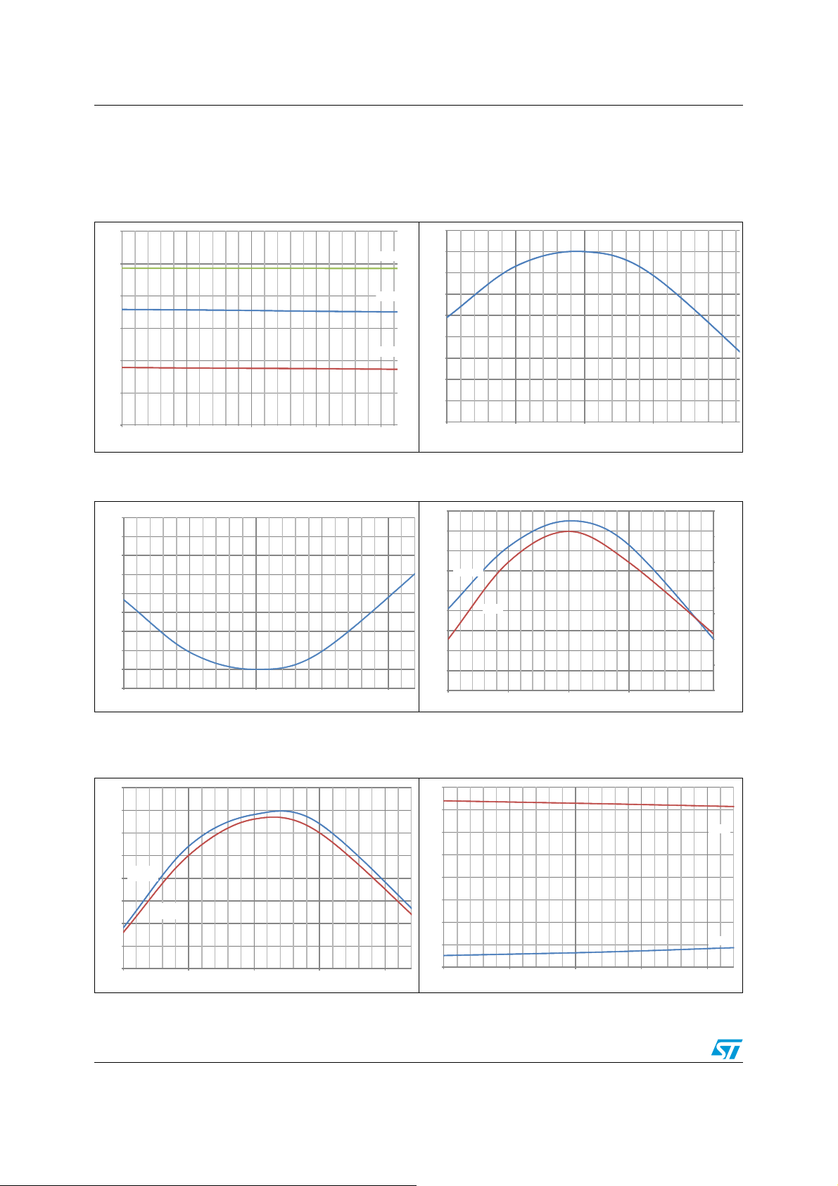
6 Typical electrical characteristics
Figure 4. VCC thresholds vs temperature Figure 5. Frequencies vs temperature
20
18
16
14
VCC Voltage
12
10
8
-25 0 25 50 75
Temperature [ C]
Vz
VCC(on)
VCC(off)
Figure 6. Times vs temperature Figure 7. FPRE resistance converter
1.04
1.035
1.03
1.025
1.02
1.015
1.01
Time intervals [normalized ]
1.005
1
0.995
-25 0 25 50 75
Temperature [ C]
1.005
1
0.995
0.99
0.985
0.98
Normalized Frequency
0.975
0.97
0.965
0.96
-25 0 25 50 75
Temper at ur e [ C]
temperature behavior
203
202
201
200
IFPRE
199
198
IFPRE [uA]
197
196
195
194
Vref
-25 0 25 50 75
Temperature [ C]
5.01
5.005
5
4.995
4.99
4.985
4.98
4.975
Vref (V)
Figure 8. IEOL vs temperature Figure 9. LSG and HSG output voltage vs
temperature (driver's current:
9.45
9.4
9.35
9.3
IEOL
9.25
(source)
9.2
IEOL (absolute value) [uA]
9.15
9.1
9.05
IEOL
(sink )
-25 0 25 50 75
Temperature [ C]
16
14
12
10
8
Vout_driver [V]
6
4
2
0
-25 0 25 50 75
14/19 Doc ID 16998 Rev 3
300mA)
Temperature [ C]
VOH
VOL

L6520, L6521 Application examples
7 Application examples
Figure 10. BJT application example
&YFF
5SUH
)35(
(2/
+%&6
3:0BGHW
9&&
+6'
/6'
*1'
5
287
Figure 11. MOSFET application example
&YFF
5VWXS
5
5VWXS
287
+9
&FS
+6
&
%/2&.
/
/6
5
(
'='=
5
+%&6
5
(
5(6
&
5(6
+9
5SUH
)35(
(2/
+%&6
3:0BGHW
&FS
+6
9&&
+6'
/6'
*1'
5
287
5
287
/6
5
(
'='=
5
+%&6
5
(
Doc ID 16998 Rev 3 15/19
&
%/2&.
/
5(6
&
5(6

Package mechanical data L6520, L6521
8 Package mechanical data
In order to meet environmental requirements, ST offers these devices in different grades of
ECOPACK
®
packages, depending on their level of environmental compliance. ECOPACK®
specifications, grade definitions and product status are available at: www.st.com.
ECOPACK is an ST trademark.
Table 8. SO-8 mechanical data
Dim.
Min Typ Max Min Typ Max
A 1.35 1.75 0.053 0.069
A1 0.10 0.25 0.004 0.010
A2 1.10 1.65 0.043 0.065
B 0.33 0.51 0.013 0.020
C 0.19 0.25 0.007 0.010
(1)
D
4.80 5.00 0.189 0.197
E 3.80 4.00 0.15 0.157
e 1.27 0.050
H 5.80 6.20 0.228 0.244
h 0.25 0.50 0.010 0.020
L 0.40 1.27 0.016 0.050
k 0° (min.), 8° (max.)
ddd 0.10 0.004
1. Dimensions D does not include mold flash, protrusions or gate burrs. Mold flash, potrusions or gate burrs
shall not exceed 0.15mm (.006inch) in total (both side).
mm. inch
16/19 Doc ID 16998 Rev 3

L6520, L6521 Package mechanical data
Figure 12. Package dimensions
Doc ID 16998 Rev 3 17/19

Revision history L6520, L6521
9 Revision history
Table 9. Document revision history
Date Revision Changes
19-Jan-2010 1 Initial release
Added: L6521 option, Section 6: Typical electrical characteristics
08-Feb-2011 2
09-Mar-2011 3 Datasheet updated from preliminary data to final datasheet
Updated: Coverpage, Figure 1, Table 4, Table 5, Section 1, Figure 3,
Table 7, Figure 10, Figure 11
18/19 Doc ID 16998 Rev 3

L6520, L6521
Please Read Carefully:
Information in this document is provided solely in connection with ST products. STMicroelectronics NV and its subsidiaries (“ST”) reserve the
right to make changes, corrections, modifications or improvements, to this document, and the products and services described herein at any
time, without notice.
All ST products are sold pursuant to ST’s terms and conditions of sale.
Purchasers are solely responsible for the choice, selection and use of the ST products and services described herein, and ST assumes no
liability whatsoever relating to the choice, selection or use of the ST products and services described herein.
No license, express or implied, by estoppel or otherwise, to any intellectual property rights is granted under this document. If any part of this
document refers to any third party products or services it shall not be deemed a license grant by ST for the use of such third party products
or services, or any intellectual property contained therein or considered as a warranty covering the use in any manner whatsoever of such
third party products or services or any intellectual property contained therein.
UNLESS OTHERWISE SET FORTH IN ST’S TERMS AND CONDITIONS OF SALE ST DISCLAIMS ANY EXPRESS OR IMPLIED
WARRANTY WITH RESPECT TO THE USE AND/OR SALE OF ST PRODUCTS INCLUDING WITHOUT LIMITATION IMPLIED
WARRANTIES OF MERCHANTABILITY, FITNESS FOR A PARTICULAR PURPOSE (AND THEIR EQUIVALENTS UNDER THE LAWS
OF ANY JURISDICTION), OR INFRINGEMENT OF ANY PATENT, COPYRIGHT OR OTHER INTELLECTUAL PROPERTY RIGHT.
UNLESS EXPRESSLY APPROVED IN WRITING BY AN AUTHORIZED ST REPRESENTATIVE, ST PRODUCTS ARE NOT
RECOMMENDED, AUTHORIZED OR WARRANTED FOR USE IN MILITARY, AIR CRAFT, SPACE, LIFE SAVING, OR LIFE SUSTAINING
APPLICATIONS, NOR IN PRODUCTS OR SYSTEMS WHERE FAILURE OR MALFUNCTION MAY RESULT IN PERSONAL INJURY,
DEATH, OR SEVERE PROPERTY OR ENVIRONMENTAL DAMAGE. ST PRODUCTS WHICH ARE NOT SPECIFIED AS "AUTOMOTIVE
GRADE" MAY ONLY BE USED IN AUTOMOTIVE APPLICATIONS AT USER’S OWN RISK.
Resale of ST products with provisions different from the statements and/or technical features set forth in this document shall immediately void
any warranty granted by ST for the ST product or service described herein and shall not create or extend in any manner whatsoever, any
liability of ST.
ST and the ST logo are trademarks or registered trademarks of ST in various countries.
Information in this document supersedes and replaces all information previously supplied.
The ST logo is a registered trademark of STMicroelectronics. All other names are the property of their respective owners.
© 2011 STMicroelectronics - All rights reserved
STMicroelectronics group of companies
Australia - Belgium - Brazil - Canada - China - Czech Republic - Finland - France - Germany - Hong Kong - India - Israel - Italy - Japan -
Malaysia - Malta - Morocco - Philippines - Singapore - Spain - Sweden - Switzerland - United Kingdom - United States of America
www.st.com
Doc ID 16998 Rev 3 19/19
 Loading...