

Page 1
Fi
查询L6388D013TR供应商
L6388
HIGH-VOLTAGE HIGH AND LOW SIDE DRIVER
1 FEATURES
■ HIGH VOLTAGE RAIL UP TO 600 V
■ dV/dt IMMUNITY ± 50 V/nsec IN FULL
TEMPERATURE RANGE
■ DRIVER CURRENT CAPABILITY:400 mA
SOURCE,650 mA SINK
■ SWITCHING TIMES 70/40 nsec RISE/FALL
WITH 1nF LOAD
■ 3.3V, 5V, 15V CMOS/TTL INPUTS
COMPARATORS WITH HYSTERESYS AND
PULL DOWN
■ INTERNAL BOOTSTRAP DIODE
■ OUTPUTS IN PHASE WITH INPUTS
■ DEAD TIME AND INTERLOCKING FUNCTION
2 DESCRIPTION
The L6388 is an high-voltage device, manufactured with the BCD"OFF-LINE" technology.
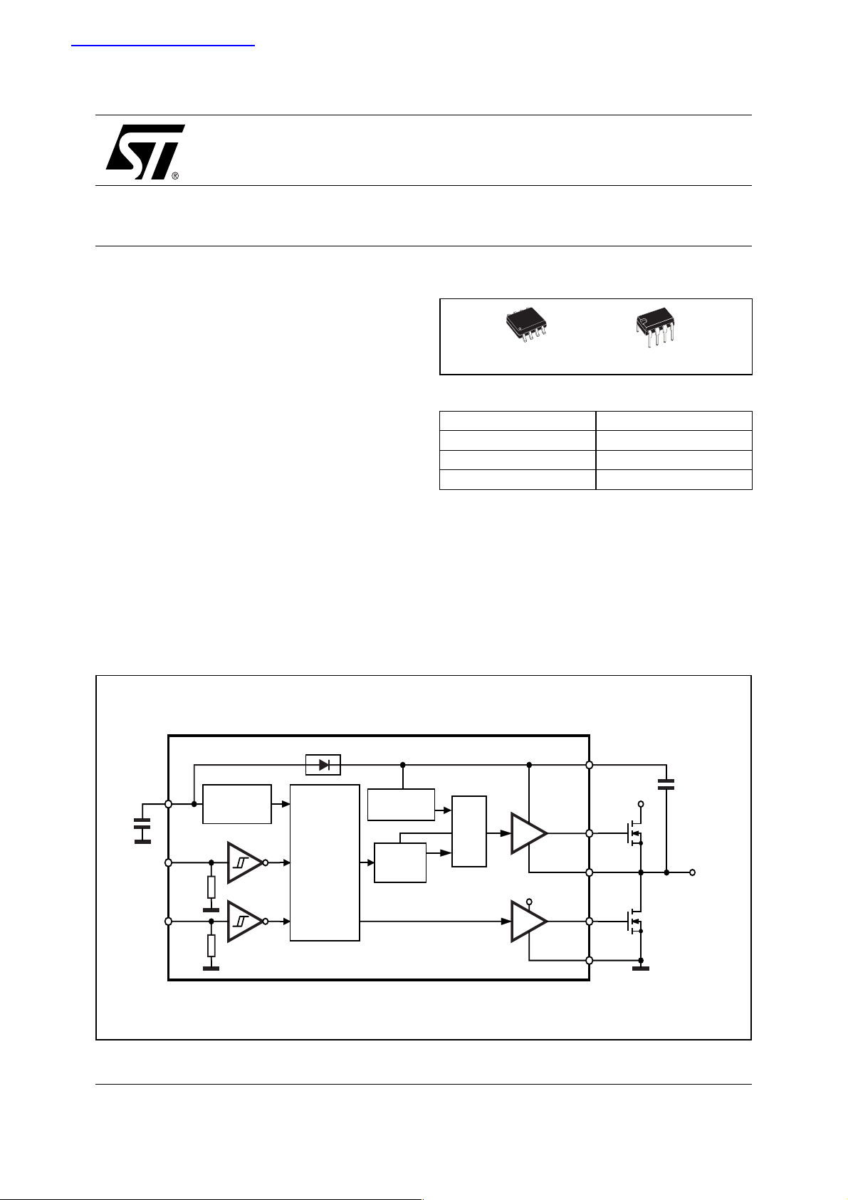
Figure 2. Block Diagram
gure 1. Package
SO8
DIP8
Table 1. Order Codes
Part Number Package
L6388 DIP8
L6388D SO8
L6388D013TR SO8 in Tape & Reel
It has a Driver structure that enables to drive independent referenced N Channel Power MOS or IGBT. The Upper (Floating) Section is enabled to
work with voltage Rail up to 600V.
The Logic Inputs are CMOS/TTL compatible for
ease of interfacing with controlling devices.
May 2005
V
CC
HIN
LIN
3
2
1
UV
DETECTION
BOOTSTRAP DRIVER
DETECTION
LOGIC
SHOOT
THROUGH
PREVENTION
UV
LEVEL
SHIFTER
R
R
S
LVG
DRIVER
V
CC
HVG
DRIVER
Vboot
8
H.V.
HVG
7
OUT
6
LVG
5
GND
4
Cboot
TO LOAD
Rev. 2
1/11
Page 2
L6388
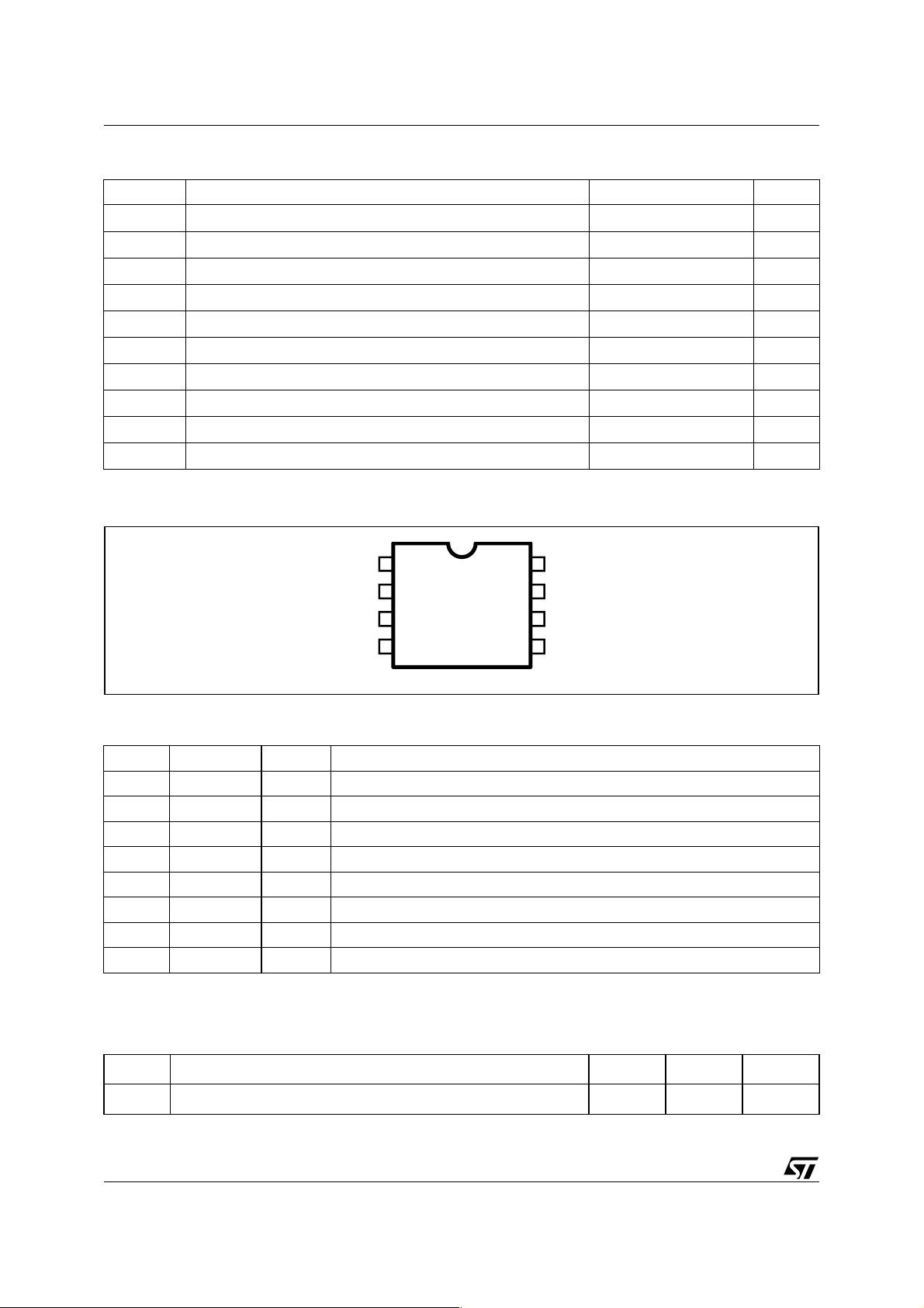
Table 2. Absolute Maximum Rating
Symbol Parameter Value Unit
V
out
V
cc
V
boot
V
hvg
V
lvg
V
dV
out
P
tot
T
T
stg
Note: ESD immunity for pins 6, 7 and 8 is guaranteed up to 900V (Human Body Model)
Output Voltage -3 to V
Supply Voltage - 0.3 to +18 V
Floating Supply Voltage - 1 to 618 V
High Side Gate Output Voltage - 1 to V
Low Side Gate Output Voltage -0.3 to Vcc +0.3 V
Logic Input Voltage -0.3 to Vcc +0.3 V
i
/dt Allowed Output Slew Rate 50 V/ns
Total Power Dissipation (Tj = 85°C) 750 mW
Junction Temperature 150 °C
j
Storage Temperature -50 to 150 °C
Figure 3. Pin Connection (Top view)
- 18 V
boot
boot
V
LIN
HIN
V
CC
GND
1
2
3
4 LVG
D97IN517A
8
7
6
5
V
boot
HVG
OUT
Table 3. Pin Description
N. Name Type Function
1 LIN I Low Side Driver Logic Input
2 HIN I High Side Driver Logic Input
3 Vcc I Low Voltage Power Supply
4 GND Ground
5 LVG (*) O Low Side Driver Output
6 OUT O High Side Driver Floating Reference
7 HVG (*) O High Side Driver Output
8 Vboot Bootstrap Supply Voltage
(*) The circuit guarantees 0.3V maximum on the pin (@ Isink = 10mA). This allows to omit the "bleeder" resistor connected between the gate
and the source of the external MOSFET normally used to hold the pin low.
Table 4. Thermal Data
Symbol Parameter SO8 Minidip Unit
R
2/11
th j-amb
Thermal Resistance Junction to Ambient 150 100 °C/W
Page 3
L6388
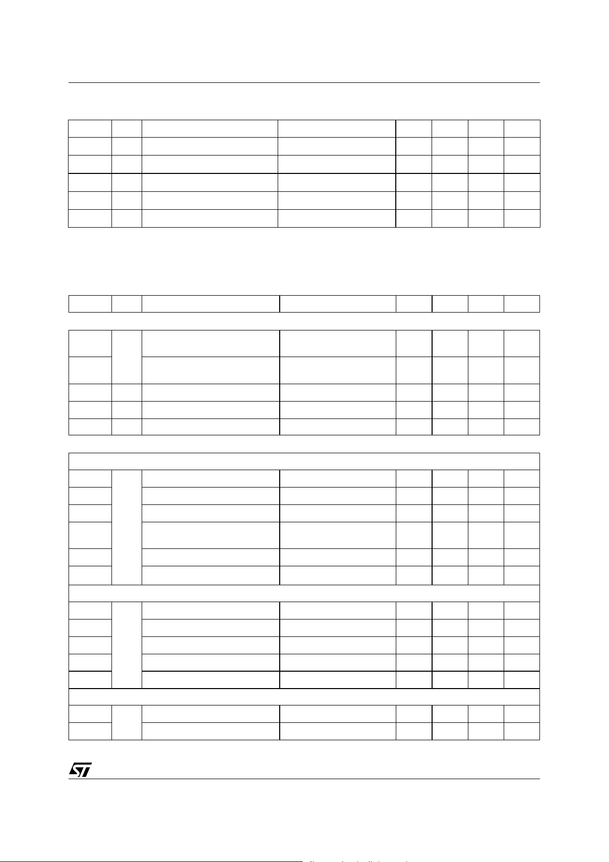
Table 5. Recommended Operating Conditions
Symbol Pin Parameter Test Condition Min. Typ. Max. Unit
V
out
V
BS
f
sw
V
cc
T
j
Note 1: If the condition Vboot - Vout < 18V is guaranteed, Vout can range from -3 to 580V
(*): VBS = Vboot - Vout
6 Output Voltage Note 1 580 V
(*) 8 Floating Supply Voltage Note 1 17 V
Switching Frequency HVG,LVG load CL = 1nF 400 kHz
3 Supply Voltage 17 V
Junction Temperature -45 125 °C
Table 6.
(V
cc
Electrical Characteristics
= 15V; Tj = 25°C)
Symbol Pin Parameter Test Condition Min. Typ. Max. Unit
AC OPERATION
t
t
DT 7,5 Dead Time 220 320 420 ns
1 vs 5
on
off
High/Low Side Driver Turn-On
2 vs 7
Propagation Delay
High/Low Side Driver Turn-Off
V
= 0V 225 300 ns
out
V
= 0V 160 220 ns
out
Propagation Delay
t
t
7,5 Rise Time CL = 1000pF 70 100 ns
r
7,5 Fall Time CL = 1000pF 40 80 ns
f
DC OPERATION
Low Supply Voltage Section
V
ccth1
V
ccth2
V
cchys
I
qccu
I
qcc
R
dson
Bootstrapped Supply Voltage Section
V
BSth1
V
BSth2
V
BShys
IQ
BS
ILK High Voltage Leakage Current V
High/Low Side Driver
I
so
I
si
3Vcc UV Turn On Threshold 9.1 9.6 10.1 V
Vcc UV Turn Off Threshold 7.9 8.3 8.8 V
Vcc UV Hysteresis 0.9 V
Undervoltage Quiescent Supply
Vcc ≤ 9V 250 330 µA
Current
Quiescent Current Vcc = 15V 350 450 µA
Bootstrap Driver on Resistance
V
cc
125 Ω
(**)
8VBS UV Turn On Threshold 8.5 9.5 10.5 V
VBS UV Turn Off Threshold 7.2 8.2 9.2 V
VBS UV Hysteresis 0.9 V
VBS Quiescent Current HVG ON 250 µA
= V
hvg
out
= V
= 600V 10 µA
boot
5,7 Source Short Circuit Current VIN = Vih (tp < 10µs) 300 400 mA
Sink Short Circuit Current VIN = Vil (tp < 10µs) 500 650 mA
3/11
Page 4
L6388
Table 6.
Electrical Characteristics (continued)
(Vcc = 15V; Tj = 25°C)
Symbol Pin Parameter Test Condition Min. Typ. Max. Unit
Logic Inputs
V
V
I
ih
I
(**) RDSON is tested in the following way:
where I1 is pin 8 current when V
1, 2 Low Level Logic Input Voltage 1.1 V
il
ih
High Level Logic Input Voltage 1.8 V
High Level Logic Input Current VIN = 15V 20 70 µA
il
Low Level Logic Input Current VIN = 0V -1 µA
VCCV
CBOOT
= V
R
DSON
CBOOT1
--------------------------------------------------------------------------------------------------------------=
I
1VCCVCCBOOT1
, I2 when V
CBOOT
–()VCCV
CBOOT1
,()I2– VCCV
= V
CBOOT2
–()–
CBOOT2
,()
CCBOOT2
.
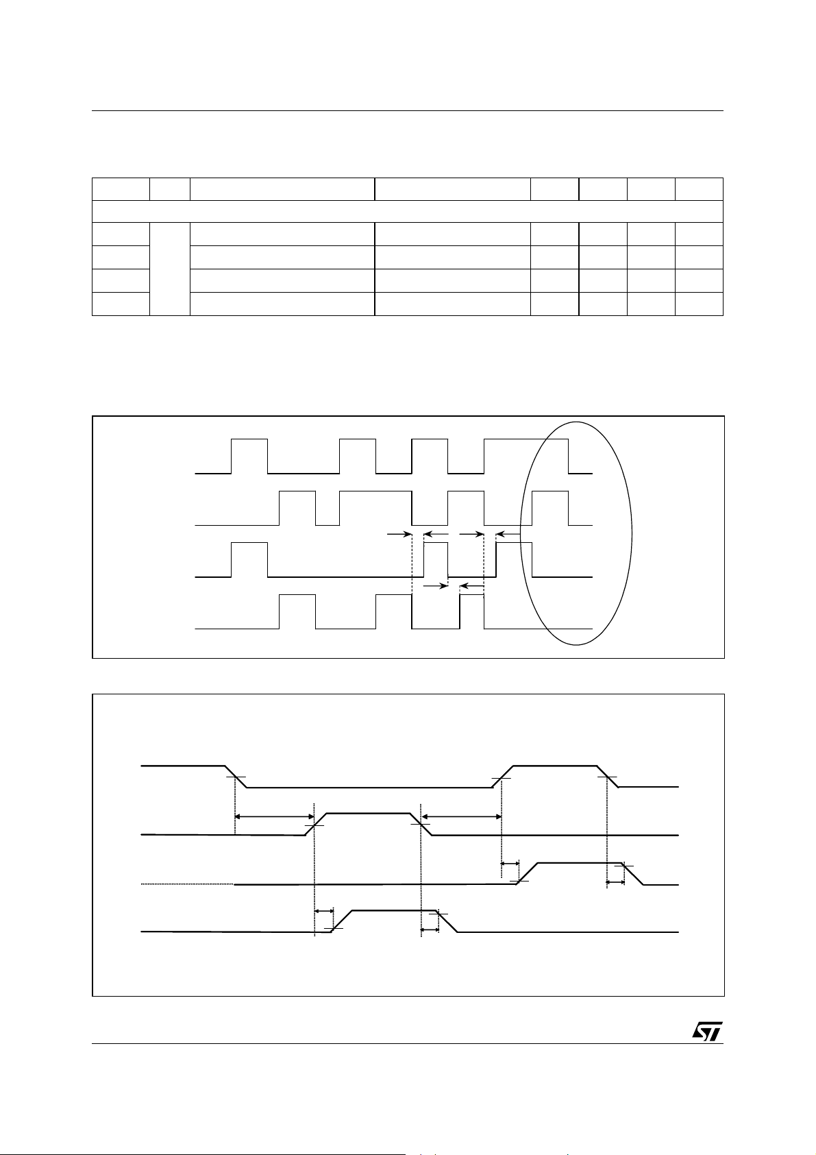
Figure 4. Dead Time Waveforms Definitions
LIN
HIN
DT DT
LVG
HVG
Figure 5. Propagation Delay Waveform Definitions
LIN
LIN
50%
50%50%
> DT
HIN
HIN
LVG
LVG
HVG
HVG
> DT
50% 50%
50% 50%50%
ton
ton
10%
10%
toff
toff
DT
> DT
> DT
90%
90%
50% 50%
50% 50%50%
ton
ton
10%
10%
Interlocking function
90%
90%
toff
toff
4/11
Page 5
L6388
3 INPUT LOGIC
Input logic is provided with an interlocking circuitry which avoids the two outputs (LVG, HVG) to be active at the
same time when both the logic input pins (LIN, HIN) are at a high logic level. In addition, to prevent cross conduction of the external MOSFETs, after each output is turned-off the other output cannot be turned-on before a
certain amount of time (DT) (see Figure 4).
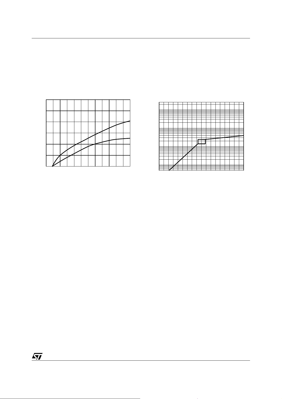
Figure 6. Typical Rise and Fall Times vs. Load
Capacitance
time
(nsec)
250
200
150
100
50
0
0 1 2 3 4 5 C (nF)
For both high and low side buffers @25˚C Tamb
D99IN1054
T
r
T
f
Figure 7. Quiescent Current vs. Supply
Voltage
Iq
(µA)
10
10
10
10
4
3
2
246810121416V
0
D99IN1055
(V)
S
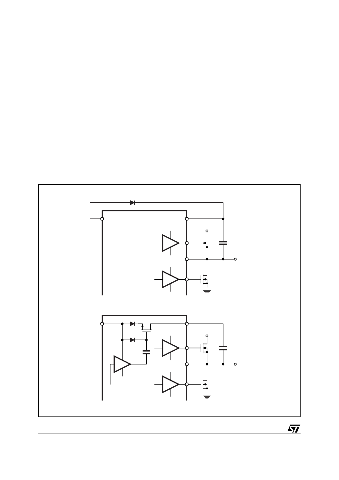
3.1 BOOTSTRAP DRIVER
A bootstrap circuitry is needed to supply the high voltage section. This function is normally accomplished by a
high voltage fast recovery diode (fig. 8a). In the L6388 a patented integrated structure replaces the external diode. It is realized by a high voltage DMOS, driven synchronously with the low side driver (LVG), with in series
a diode, as shown in fig. 8b
An internal charge pump (fig. 8b) provides the DMOS driving voltage .
The diode connected in series to the DMOS has been added to avoid undesirable turn on of it.
3.2 CBOOT selection and charging
To choose the proper C
C
is related to the MOS total gate charge :
EXT
The ratio between the capacitors C
value the external MOS can be seen as an equivalent capacitor. This capacitor
BOOT
Q
-------------- -=
V
gate
gate
EXT
and C
C
EXT
is proportional to the cyclical voltage loss .
BOOT
It has to be:
CBOOT>>>CEXT
e.g.: if Q
is 30nC and V
gate
is 10V, C
gate
is 3nF. With C
EXT
= 100nF the drop would be 300mV.
BOOT
If HVG has to be supplied for a long time, the CBOOT selection has to take into account also the leakage losses.
e.g.: HVG steady state consumption is lower than 200
C
. This charge on a 1µF capacitor means a voltage drop of 1V.
EXT
µ
A, so if HVG TON is 5ms, CBOOT has to supply 1µC to
The internal bootstrap driver gives great advantages: the external fast recovery diode can be avoided (it usually
has great leakage current). This structure can work only if V
the LVG is on. The charging time (T
charge
) of the C
BOOT
is close to GND (or lower) and in the meanwhile
OUT
is the time in which both conditions are fulfilled and it
5/11
Page 6
L6388
has to be long enough to charge the capacitor.
The bootstrap driver introduces a voltage drop due to the DMOS RDSON (typical value: 125 Ohm). At low fre-
quency this drop can be neglected. Anyway increasing the frequency it must be taken in to account.
The following equation is useful to compute the drop on the bootstrap DMOS:
Q
V
→
drop
dson
where Q
and T
charge
==
V
dropIch eargRdson
is the gate charge of the external power MOS, R
gate
is the charging time of the bootstrap capacitor.
For example: using a power MOS with a total gate charge of 30nC the drop on the bootstrap DMOS is about
1V, if the T
is 5µs. In fact:
charge
V
drop
30nC
-------------- - 125 Ω 0.8V∼⋅=
5µs
gate
------------------- - R
T
ch earg
dson
is the on resistance of the bootstrap DMOS,
has to be taken into account when the voltage drop on C
V
drop
is calculated: if this drop is too high, or the
BOOT
circuit topology doesn't allow a sufficient charging time, an external diode can be used.
Figure 8. Bootstrap Driver.
D
BOOT
V
S
HVG
LVG
V
V
BOOT
OUT
H.V.
C
BOOT
TO LOAD
a
V
V
S
BOOT
H.V.
6/11
b
HVG
LVG
C
BOOT
V
OUT
TO LOAD
Page 7
L6388
)
)
)
)
)
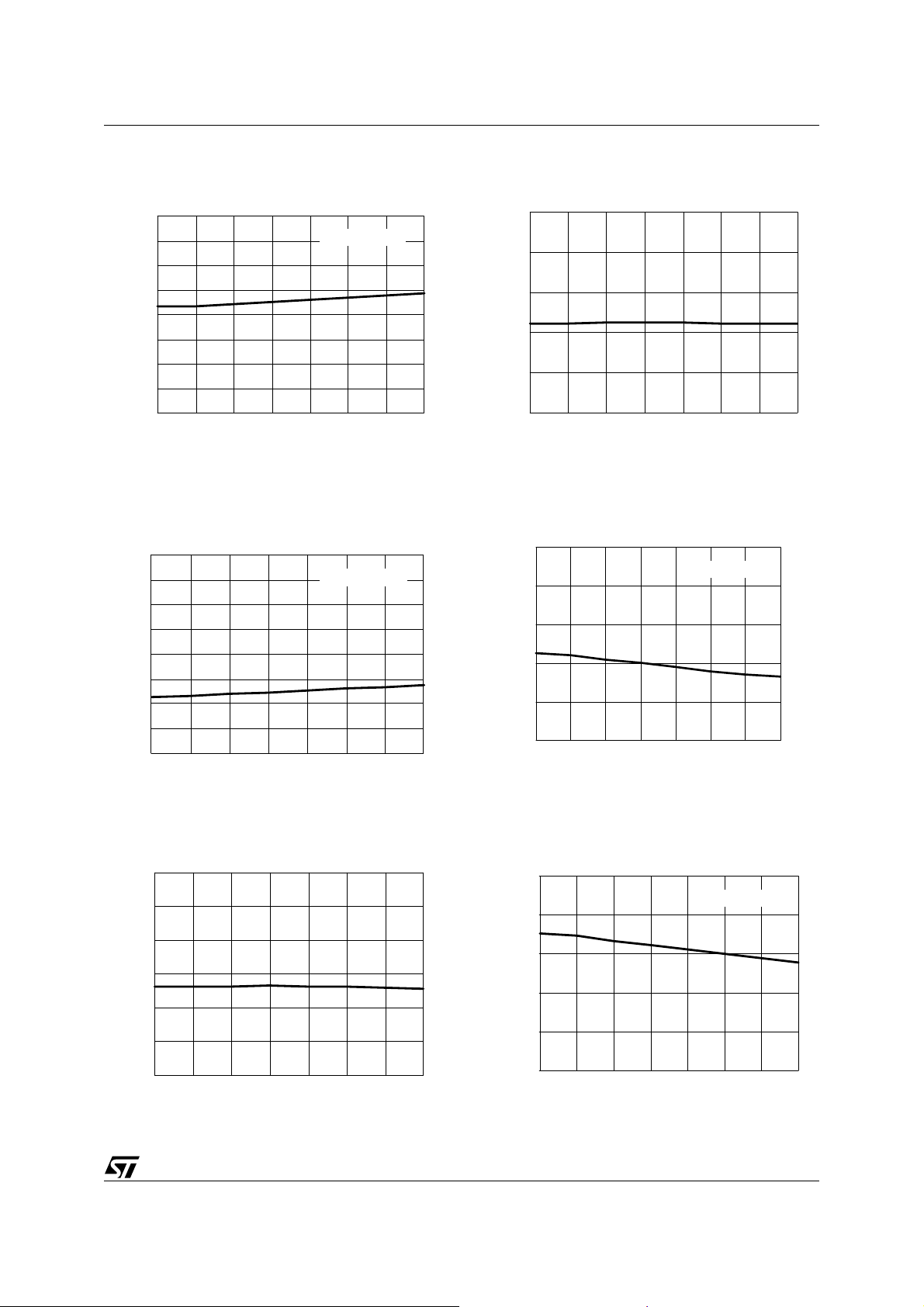
Figure 9. V
UV Turn On Threshold vs.
BOOT
Temperature
13
12
11
Typ.
10
(V)
9
BSth1
8
V
7
6
5
-45 -25 0 25 50 75 100 125
Tj (˚C
Figure 10. V
UV Turn Off Threshold vs.
BOOT
@ Vcc = 15V
Temperature
14
13
12
11
(V)
10
9
BSth2
V
8
Typ.
7
6
-45 -25 0 25 50 75 100 125
@ Vcc = 15V
Figure 12. V
UV Turn Off Threshold vs.
CC
Temperature
11
10
9
Typ.
8
Vccth2(V)
7
6
-45 -25 0 25 50 75 100 125
Tj (˚C
Figure 13. Output Source Current vs.
Temperature
1000
@ Vcc = 15V
800
600
Typ.
400
current (mA)
200
0
-45-25 0 255075100125
Tj (˚C
Figure 11. V
UV Turn On Threshold vs.
CC
Temperature
13
12
11
10
Typ.
Vccth1(V)
9
8
7
-45 -25 0 25 50 75 100 125
Tj (˚C
Figure 14. Output Sink Current vs.
Temperature
1000
@ Vcc = 15V
800
600
Typ.
400
current (mA)
200
0
-45 -25 0 25 50 75 100 125
Tj (˚C
7/11
Page 8
L6388
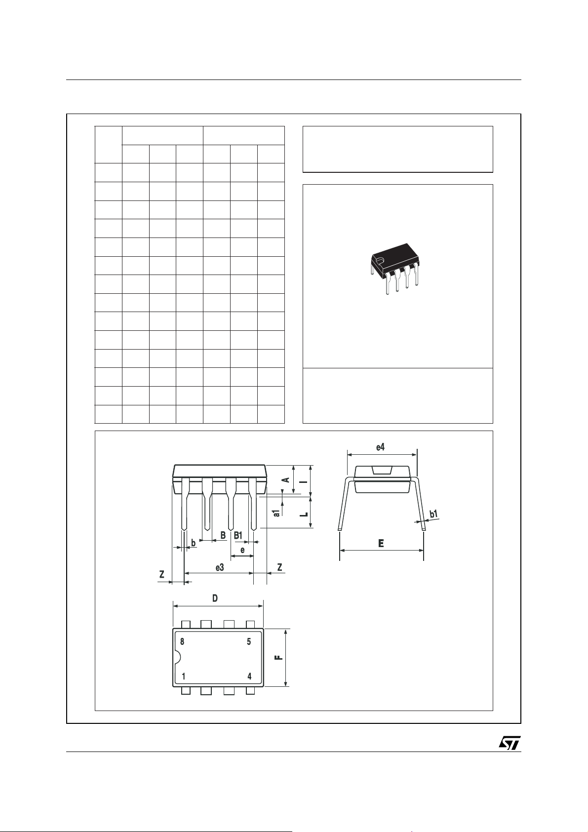
Figure 15. DIP8 Mechanical Data & Package Dimensions
DIM.
mm inch
MIN. TYP. MAX. MIN. TYP. MAX.
A3.32 0.131
a1 0.51 0.020
B 1.15 1.65 0.045 0.065
b 0.356 0.55 0.014 0.022
b1 0.204 0.304 0.008 0.012
D 10.92 0.430
E 7.95 9.75 0.313 0.384
e2.54 0.100
e3 7.62 0.300
e4 7.62 0.300
F 6.6 0.260
I 5.08 0.200
L 3.18 3.81 0.125 0.150
Z 1.52 0.060
OUTLINE AND
MECHANICAL DATA
DIP-8
8/11
Page 9
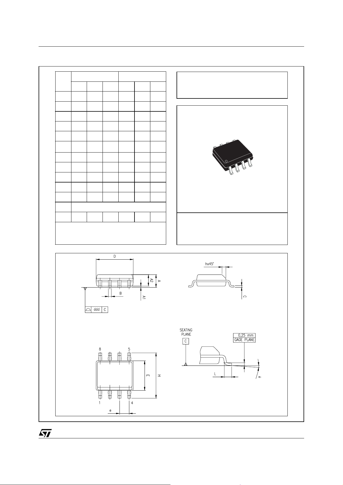
Figure 16. SO8 Mechanical Data & Package Dimensions
L6388
DIM.
A 1.35 1.75 0.053 0.069
A1 0.10 0.25 0.004 0.010
A2 1.10 1.65 0.043 0.065
B 0.33 0.51 0.013 0.020
C 0.19 0.25 0.007 0.010
(1)
D
E 3.80 4.00 0.15 0.157
e 1.27 0.050
H 5.80 6.20 0.228 0.244
h 0.25 0.50 0.010 0.020
L 0.40 1.27 0.016 0.050
k 0˚ (min.), 8˚ (max.)
ddd 0.10 0.004
Note: (1) Dimensions D does not include mold fla sh, protru-
mm inch
MIN. TYP. MAX. MIN. TYP. MAX.
4.80 5.00 0.189 0.197
sions or gate burrs.
Mold flash, potrusions or gate burrs sh all not exceed
0.15mm (.006inch) in total (both side).
OUTLINE AND
MECHANICAL DATA
SO-8
0016023 C
9/11
Page 10
L6388
Table 7. Revision History
Date Revision Description of Changes
January 2005 1 First Issue
May 2005 2 Changed from Preliminary Data to Final
10/11
Page 11

L6388
Information furnished is believed to be accurate and reliable. However, STMicroelectronics assumes no responsibility for the consequences
of use of such information nor for any infringement of patents or other rights of third parties which may result from its use. No license is granted
by implication or otherwise under any patent or patent rights of STMicroelectronics. Specifications mentioned in this publication are subject
to change without notice. This publication supersedes and replaces all information previously supplied. STMicroelectronics products are not
authorized for use as critical components in life support devices or systems without express written approval of STMicroelectronics.
The ST logo is a registered trademark of STMicroelectronics.
All other names are the property of their respective owners
© 2005 STMicroelectronics - All rights reserved
Australia - Belgium - Brazil - Canada - China - Czech Republic - Finland - France - Germany - Hong Kong - India - Israel - Italy - Japan -
Malaysia - Malta - Morocco - Singapore - Spain - Sweden - Switzerland - United Kingdom - United States of America
STMicroelectronics group of companies
www.st.com
11/11
 Loading...