

Page 1
CURRENTCONTROLLERFOR STEPPING MOTORS
DESCRI P TI ON
The L6506/Dis a linearintegratedcircuit designed
to senseand controlthecurrentinsteppingmotors
and similardevices.Whenusedin conjunctionwith
the L293, L298, L7150,L6114/L6115,the chip set
formsa constantcurrentdrive foran inductiveload
andperformsalltheinterfacefunctionfromthe control logic thruthe powerstage.
Two or more devices may be synchronized using
thesyncpin.In thismodeof operationtheoscillator
in themasterchipsetstheoperatingfrequencyinall
chips.
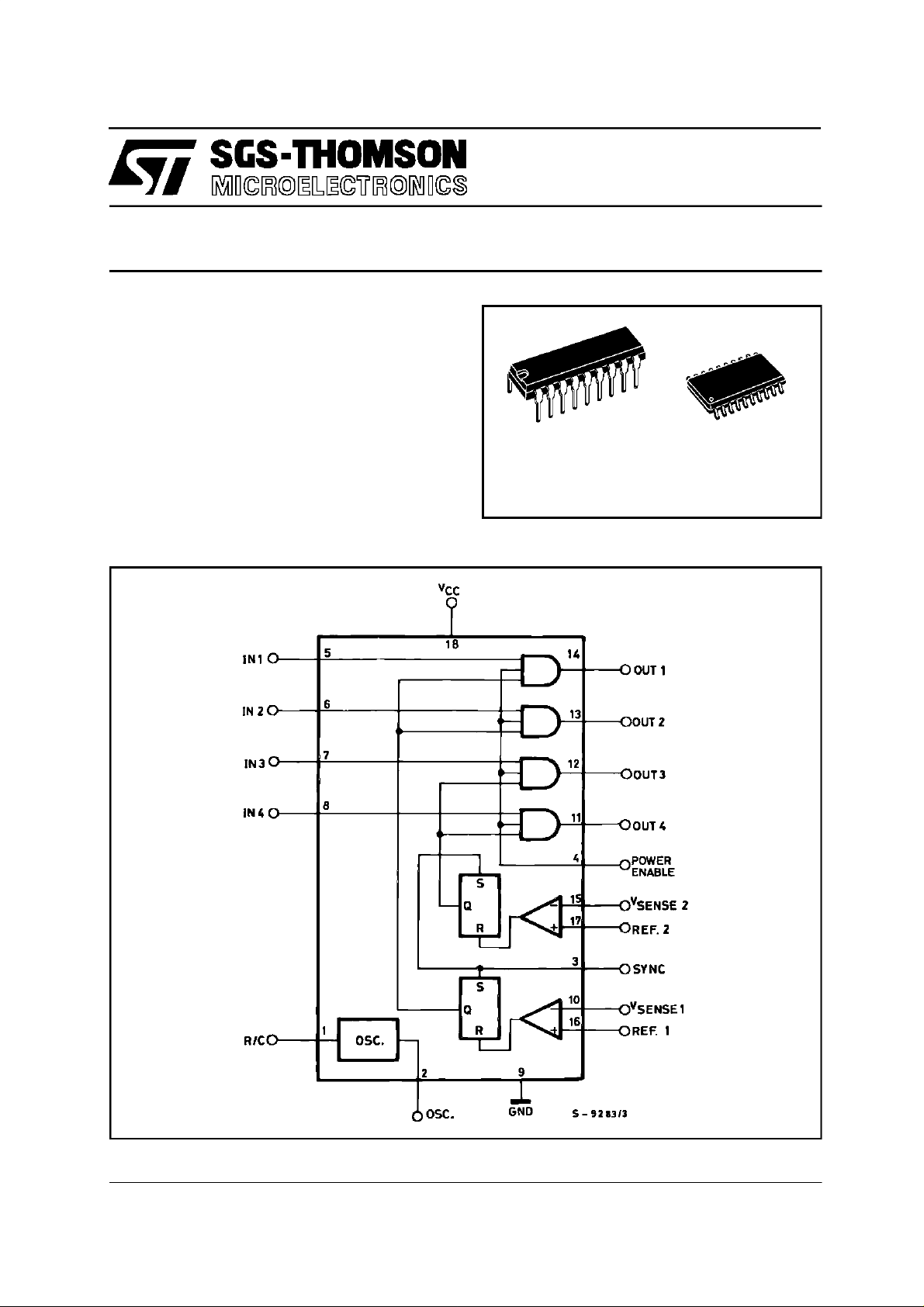
BLOCK DIAGRAM (pin’s number referred to DIP-18)
L6506
L6506D
DIP18 SO20
ORDERING NUMBERS:
L6506 L6506D
June 1997
1/8
Page 2
L6506 -L6506D
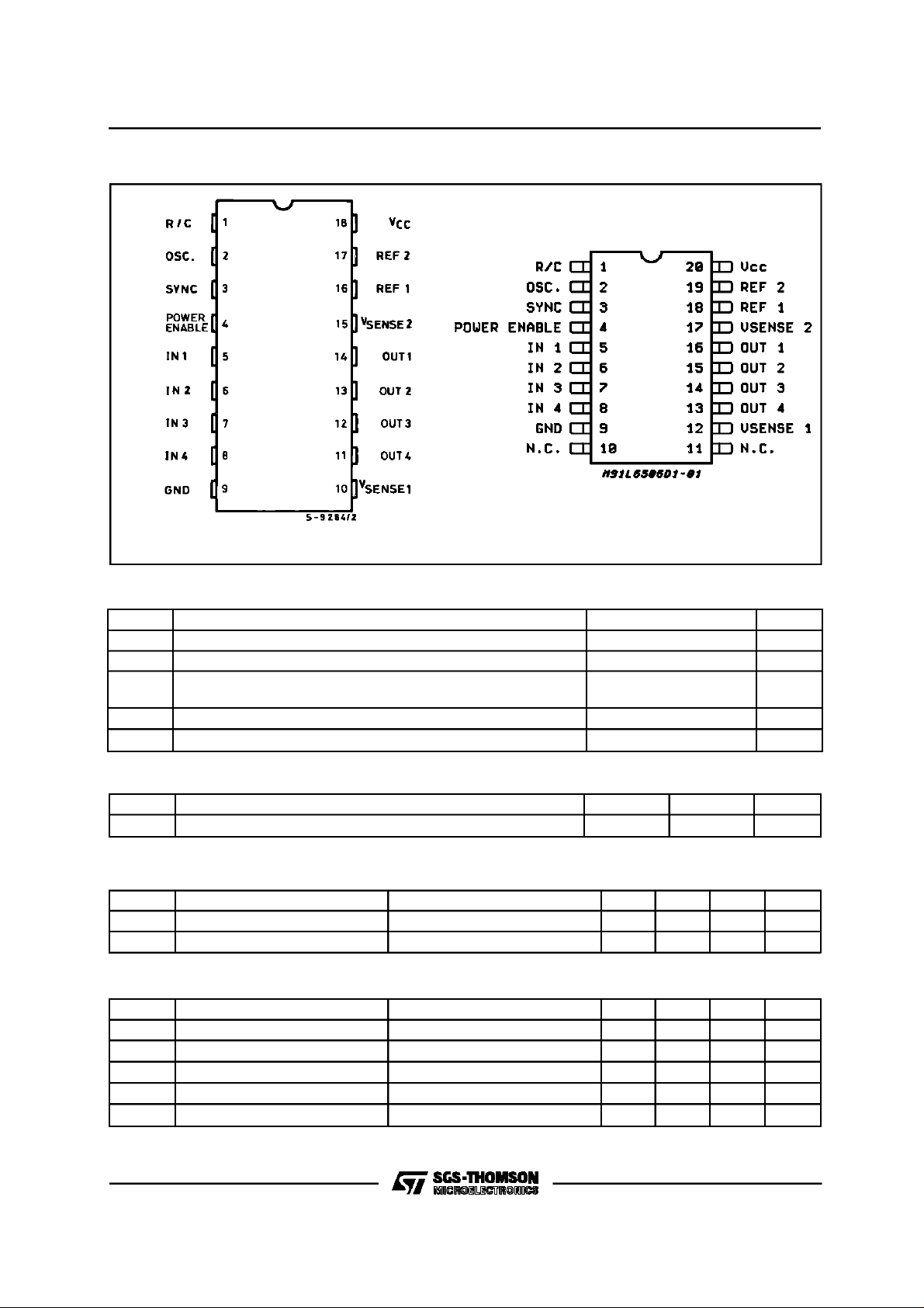
PI N CONNE CTI ONS (top view)
DIP18 SO20
ABSOLUTEMAXIMUM RATINGS
Symbol Parameter Val u e Uni t
V
V
P
T
T
Supply Voltage 10 V
CC
Input Signals 7 V
i
Total Power Dissipation(T
tot
=70°C) for DIP18
amb
Total Power Dissipation(Tamb =70ÉC) for SO20
JunctionTemperature 150
j
Storage Temperature -40 to 150
stg
1
0.8
THERMAL DATA
Symb o l Parameter DIP 18 SO 20 Uni t
R
thj-amb
ELECTRICAL CHARACTERESTICS (VCC= 5.0V,T
Thermal ResistanceJunction-ambient Max. 80 100
=25°C; unlessotherwisenoted)
amb
C/W
°
Symb o l Parameter Test Cond itions Mi n . Typ . Max. Unit
V
I
SupplyVoltage 4.5 7 V
CC
QuiescentSupplyCurrent VCC=7V 25 mA
CC
COMPARATOR SECTION
Symb o l Parameter Test Cond itions Mi n . Typ . Max. Unit
V
V
I
I
Input Voltage Range V
IN
Input Offset Voltage VIN= 1.4V
IO
Input Offset Current
IO
Input Bias Current 1 µ
IB
Response time V
Inputs –0.3 3 V
sense
±5.0
±200
REF
= 1.4V V
= 0 to 5V 0.8 1.5
SENS
W
W
C
°
°C
mV
nA
µ
A
s
2/8
Page 3
L65 06 - L6506D
ELECTRICAL CHARACTERISTICS(continued)
COMPARATOR SECTIONPERFORMANCE(OverOperatingTemperatureRange)
Symbol Parameter Test Condtions Min. Typ. Max. Unit
V
Input Offset Voltage VIN= 1.4V
IO
Input Offset Curent
I
IO
±
±
500
20
mV
nA
LOGICSECTION
Symbol Parameter Test Condtions Min. Typ. Max. Unit
V
V
V
Input High Voltage 2 V
IH
Input Low Voltage 0.8 V
V
IL
Output High Voltage VCC= 4.75V
OH
Ouptut Low Voltage VCC= 4.75V
OL
Ouput Source Current - Outputs
I
OH
1-4
(OverOperatingTemperatureRange -TTL compatibleinputs& outputs)
2 3.5 V
= 400µA
I
OH
0.25 0.4 V
= 4mA
I
OH
VCC= 4.75V 2.75 mA
s
OSCILLATOR
Symbol Parameter Test Condtions Min. Typ. Max. Unit
f
V
V
Frequency Range 5 70 KHz
osc
Lower Threshold Voltage 0.33 V
thL
Higher Threshold Voltage 0.66 V
thH
Internal Discharge Resistor 0.7 1 1.3
R
i
CC
CC
CIRCUIT OP ERATION
TheL6506isintendedfor use withdual bridgedrivers,suchasthe L298,quaddarlingtonarrays,such
as the L7150, quad DMOS array such as L6114L6115,ordiscretepowertransistorstodrivestepper
motorsandothersimilarloads.Themainfunctionof
thedeviceistosenseandcontrolthecurrentineach
of theload windings.
Acommonon-chiposcillatordrivesthedualchopper
andsetsthe operatingfrequencyforthepulsewidth
modulateddrive.The RCnetworkon pin1 setsthe
operatingfrequencywhichis givenby the equation
:
f = forR > 10 K
1
0.69 RC
The oscillator provides pulses to set the two flipflopswhichin turncausethe outputsto activatethe
drive.Whenthecurrentintheloadwindingreaches
theprogrammedpeakvalue,thevoltageacrossthe
senseresistor (R
) is equal to V
sense
and the cor-
ref
respondingcomparatorresetsits flip-flopinterruptingthedrivecurrentuntilthenextoscillatorpulseoccurs. The peak current in each winding is programmedby selectingthe valueofthe senseresis-
tor and V
. Sinceseparateinputsare providedfor
ref
each chopper, each of the loads may be programmed independentlyallowing the device to be
used to implement microstepping of the motor.
LowerthresholdofL6506’soscillatoris 1/3V
per thresholdis 2/3 V
sistoris 1 KΩ ±
30%.
and internal dischargere-
CC
CC
Ground noise problems in multiple configurations
can be avoided by synchronizing the oscillators.
This may be done by connecting the sync pins of
eachof the deviceswith the oscillatoroutput of the
masterdeviceandconnectingtheR/Cpinoftheunusedoscillatorsto ground.
Theequationsfor the activetime of thesync pulse
(T2),the inactivetimeof thesyncsignal(T1)andthe
dutycyclecanbefoundbylookingatthefigure1 and
are:
R1R
T2 = 0.69C1 (1)
R1 + R
IN
IN
T1 = 0.69 R1C1 (2)
DC= (3)
T2
T1 + T2
V
V
V
kΩ
.Up-
3/8
Page 4

L6506 -L6506D
By substituting equations1 and 2 into equation 3
and solving for the value of R1 the followingequationsfor theexternal componentscan bederived :
R1 = ( –2) R
1
DC
C1 = (5)
0.69R1
IN
T1
(4)
Figure1 : OscillatorCircuitandWaveforms.
Lookingat equation1 itcan easilybe seen thatthe
minimumpulsewidthof T2willoccurwhenthevalue
of R1 is at its minimum and the valueof R1 at its
maximum. Therefore, when evaluatingequation 4
the minimum value for R1 of 700Ω (1KΩ –30%)
should be used to guarantee the required pulse
width.
APPL ICATI ONS INFO RMATION
Thecircuits shown infigure2 use theL6506 toimplementconstantcurrentdrivesforsteppermotors.
Figure 2 shows the L6506 used with the L298 to
drivea 2 phasebipolarmotor. Thepeakcurrentcan
be calculatedusingthe equation:
V
I
peak
ref
=
R
sense
The circuit of Fig.2 can be used in applicationsrequiring different peak and hold current values by
modifyingthe referencevoltage.
TheL6506maybeusedtoimplementeitherfullstep
or half step drives. In the case of 2 phase bipolar
stepper motor applications, if a half step drive is
used,thebridge requiresan additionalinput todisablethe power stageduringthe half step.Ifusedin
conjunctionwith the L298the enableinputsmaybe
usedfor this purpose.
Forquad darlingtonarrayin 4 phaseunipolarmotor
applications half step may be implemented using
the 4 phaseinputs.
The L6506 may also be used to implement microsteppingof either bipolaror unipolarmotors.
4/8
Page 5

L65 06 - L6506D
Figure2 : ApplicationCircuit BipolarStepperMotorDriver.(pin’s numberreferredto DIP18)
5/8
Page 6

L6506 -L6506D
DIP18PACKAGE MECHANICAL DATA
DIM.
MIN. TYP. MAX. MIN. TYP. MAX.
a1 0.254 0.010
B 1.39 1.65 0.055 0.065
b 0.46 0.018
b1 0.25 0.010
D 23.24 0.915
E 8.5 0.335
e 2.54 0.100
e3 20.32 0.800
F 7.1 0.280
I 3.93 0.155
L 3.3 0.130
Z 1.27 1.59 0.050 0.063
mm inch
6/8
Page 7

SO20PACKAGEMECHANICAL DATA
L65 06 - L6506D
DIM.
MIN. TYP. MAX. MIN. TYP. MAX.
A 2.65 0.104
a1 0.1 0.3 0.004 0.012
a2 2.45 0.096
b 0.35 0.49 0.014 0.019
b1 0.23 0.32 0.009 0.013
C 0.5 0.020
c1 45 (typ.)
D 12.6 13.0 0.496 0.512
E 10 10.65 0.394 0.419
e 1.27 0.050
e3 11.43 0.450
F 7.4 7.6 0.291 0.299
L 0.5 1.27 0.020 0.050
M 0.75 0.030
S 8 (max.)
mm inch
7/8
Page 8

L6506 -L6506D
Information furnished is believed to be accurate and reliable. However, SGS-THOMSON Microelectronics assumes no responsibility for
the consequences of use of such information nor for any infringement of patents or other rights of third parties which may result from its
use. No license is granted by implication or otherwise under any patent or patent rights of SGS-THOMSON Microelectronics. Specification
mentioned in this publication are subject to change without notice. This publication supersedes and replaces all information previously
supplied. SGS-THOMSON Microelectronics products are not authorized for use as critical components in life support devices or systems
withoutexpress written approval of SGS-THOMSON Microelectronics.
Australia - Brazil - Canada - China - France - Germany - Hong Kong - Italy - Japan - Korea - Malaysia - Malta - Morocco -
The Netherlands - Singapore - Spain - Sweden - Switzerland - Taiwan - Thailand - United Kingdom - U.S.A.
1997 SGS-THOMSON Microelectronics – Printed in Italy – All Rights Reserved
SGS-THOMSON Microelectronics GROUP OF COMPANIES
8/8
 Loading...