

Page 1
Dual 13x16 Matrix Head Ink Jet Driver
PQFP100
Features
■ DRIVES TWO 13X16 MATRIX HEADS
■ HEAD TEMPERATURE SENSING
■ POWER UP SYSTEM
■ ELECTRICAL NOZZLE CHECK
■ 8 BIT A/D
■ 5 BIT D/A
■ ± 4KV ESD PROTECTED OUTPUTS
Description
L6452 is a device designed to drive two 13x16
matrix ink jet print heads in printer applications.
The output stage is able to source simultaneously
400 mA on each of the 16 power lines (columns)
with a duty cycle of 33% in normal printing and
66% in head pre-heating. On the address lines
(rows), the load is only capacitive (MOS FET
driving capability). The driver can control two print
heads, but only one is active at a time. The
address scanning counter is included and can be
disabled to allow a different scanning scheme.
L6452
In order to avoid output activation during the
supply transient, an internal power-up system is
implemented.
As supporting function, L6452 is capable of
sensing the head silicon temperature and to
electrically check each nozzle.
The device is also integrating a thermal
protection
.
Order codes
Part number Op. Temp range, ° CPackage Packing
E-L6452 0 to 70 PQFP100 Tray
L6452DIE8 0 to 70 DIE --
Rev 2
February 2006 1/22
www.st.com
22
Page 2

Contents L6452
Contents
1 Block diagrams . . . . . . . . . . . . . . . . . . . . . . . . . . . . . . . . . . . . . . . . . . . . . . . 3
2 Pin description . . . . . . . . . . . . . . . . . . . . . . . . . . . . . . . . . . . . . . . . . . . . . . . . 5
3 Electrical specifications . . . . . . . . . . . . . . . . . . . . . . . . . . . . . . . . . . . . . . . . 8
3.1 Absolute maximum ratings . . . . . . . . . . . . . . . . . . . . . . . . . . . . . . . . . . . . . . . 8
3.2 DC Electrical characteristics . . . . . . . . . . . . . . . . . . . . . . . . . . . . . . . . . . . . . . 8
3.3 Counter Truth Table . . . . . . . . . . . . . . . . . . . . . . . . . . . . . . . . . . . . . . . . . . . . 12
3.4 Decoder Truth Table . . . . . . . . . . . . . . . . . . . . . . . . . . . . . . . . . . . . . . . . . . . 13
4 Print Head Temperature Control Part . . . . . . . . . . . . . . . . . . . . . . . . . . . . 14
4.1 Introduction . . . . . . . . . . . . . . . . . . . . . . . . . . . . . . . . . . . . . . . . . . . . . . . . . . 14
4.2 Print Head Block Diagram (Figure 5.) . . . . . . . . . . . . . . . . . . . . . . . . . . . . . . 14
5 Package information . . . . . . . . . . . . . . . . . . . . . . . . . . . . . . . . . . . . . . . . . . 20
6 Revision history . . . . . . . . . . . . . . . . . . . . . . . . . . . . . . . . . . . . . . . . . . . . . . 21
2/22
Page 3
L6452 Block diagrams
PRINT HEAD
DRIVER
PRINT HEAD
TEMPERATURE
CONTROL
POWER &
LOGICAL
SUPPLIES
CONTROL
LINES
A/D & PRINT HEAD
TEMPERATURE
CONTROL LINES
ANALOG
INPUTS
PRINT HEAD
A
PRINT HEAD
B
D97IN523
13 ADDRESS LINES
CHANNEL B
16 POWER LINES
13 ADDRESS LINES
CHANNEL A
NCEN
TRIGGER
LONGPULSE
SHORTPULSE
DATA BIT 15
DATA BIT 1
DATA BIT 0
1
0
NCOUT
OUTPUT15
OUTPUT1
OUTPUT0
Va
D97IN525B
1.25mA
FROM 16 BIT
DATA LATCH
1 Block diagrams
Figure 1. Block diagram
Figure 2. Block Diagram: Power Line Output Stage.
3/22
Page 4
16 BIT SERIAL
INPUT &
PARALLEL
OUTPUT
16 BIT LATCH
16 POWER
OUTPUT
STAGES
OUTPUT0
OUTPUT1
OUTPUT2
OUTPUT3
OUTPUT4
OUTPUT5
OUTPUT6
OUTPUT7
OUTPUT8
OUTPUT9
OUTPUT10
OUTPUT11
OUTPUT12
OUTPUT13
OUTPUT14
OUTPUT15
NCOUT
SDI
SDC
LATCHCLEAR
LATCHDATA
NCEN
LONGPULSE
SHORTPULSE
SELECTOR
4 to 13 LINES
DECODER
13 MOS
DRIVERS
CHANNEL A
HSA1
ENIC
S3
UPC/S2
RESC/S1
CLKC/S0
HSA2
HSA3
HSA4
HSA5
HSA6
HSA7
HSA8
HSA9
HSA10
HSA11
HSA12
HSA13
13 MOS
DRIVERS
CHANNEL B
HSB1
HSB2
HSB3
HSB4
HSB5
HSB6
HSB7
HSB8
HSB9
HSB10
HSB11
HSB12
HSB13
C0
C1
C2
C3
0 to 13
UP/DOWN
COUNTER
CHSEL
ENCH
D97IN524A
Block diagrams L6452
Figure 3. Block Diagram: Nozzle activation part
4/22
Page 5
L6452 Pin description
1
2
3
5
6
4
7
8
9
10
361137 38 39 40 41
95 94 93 929091 89 88 87 86 85
70
69
68
66
65
67
75
74
73
71
72
OUTPUT13
OUTPUT14
POWGND
OUTPUT15
CRLATCH
V
C
OUTPUT10
V
C
OUTPUT11
V
C
OUTPUT12
RESET
CONVSTART
ADCK
NCOUT
ADDATA
CH0BUF
ANALOGND
ADCGND
V
a
VREF
CH5
RXA
RXB
REXT
CSGND
V
a
VDDVSTEP-UP
STEPUPBOOST
STEPUPGND
CLKC/S0
ENCH
HSA4
HSA5
HSA6
HSA8
HSA9
HSA7
ENIC
GND
HSA1
HSA3
HSA2
D97IN489C
96
VXA
97
VXB
98
ONENABLE
99
CRCLOCK
100
CRDATA
LATCHDATA
SDI
SDC
LONGPULSE
31 32 33 34 35
64
63
61
60
62
HSA10
HSA11
HSA13
V
r
HSA12
12
13
14
15
16
OUTPUT7
POWGND
OUTPUT8
OUTPUT9
V
C
17
18
19
20
V
C
OUTPUT5
OUTPUT6
V
C
21
22
23
24
25
OUTPUT1
OUTPUT2
V
C
OUTPUT4
OUTPUT3
59
57
56
58
HSB13
HSB11
HSB10
HSB12
HSB9
HSB8
HSB6
HSB5
HSB7
45 46 47 48 49
50
84 838182
CH4
CH3
CH1
CH2
RESC/S1
UPC/S2
CHSEL
S3
42 43 44
26
27
28
29
30
NCEN
LATCHCLEAR
OUTPUT0
V
C
POWGND
55
54
52
51
53
HSB4
HSB3
HSB1
GND
HSB2
80
79
78
76
77
2 Pin description
Figure 4. Pin connection (Top view)
Table 1. Pin function
Pin # Name Function
1 CRlatch
2, 5, 6, 8, 9,
11, 12, 14,
16, 18, 19,
21, 22, 24,
25, 28
Output15...0
A rising edge transfer the information from CR shift register into the
control register latching the data on the falling edge
High side DMOS outputs. To be active, ShortPulse and/or LongPulse
and NcEn must have a low level
5/22
Page 6
Pin description L6452
Table 1. Pin function - continued
Pin # Name Function
3, 7, 10, 13,
17, 20, 23,
26
4, 15, 27,
51, 79, 92
29 LatchClear A high level resets all bit in the latch
30 NcEn
Vc
GND logic and power ground
Outputs Power Supply
A high level enables the internal current sources and disables all
DMOS outputs. To be active, the internal current sources must have
their corresponding bit set in the 16 bit latch and
set to low level. This function is called Nozzle Check Enable.
LongPulse must be
31 LatchData
32 SDI Serial data input of the shift register
33 SDC
34 LongPulse
35 ShortPulse
36 Reset A low level disables all functions and clears all registers
37 ConvStart A high level enables the A/D to start the new conversion
38 ADCK
39 NCOut
40 CH0buf Analog output signal (CH0 buffered)
41 ADDATA A/D serial data output
42 AnalogGND Analog ground connection
43 ADCGND Ground of internal ADC
A rising edge latches the 16 bit stored in the shift register in the 16 bit
latch
The data bit presented to the SDI pin is stored into the register on the
rising edge of this pin
A low level activates all outputs having their corresponding bit in the
16 bit latch set (this pin has an internal pull-up resistor)
A low level activates all outputs having their corresponding bit in the
16 bit latch reset (this pin has an internal pull-up resistor)
A/D clock signal; the ADDATA signal are valid on the falling edge of
this pin
If NcEn is high this output provides a high level when the open load is
detected on the output. If NcEn is low this output provides a high level
when a short circuit is detected on HSA/B output
44, 90 Va Power supply
45 Vref Reference voltage generator
46 to 50 CH5..CH1 A/D input signals
52 to 64 HSB1..HSB13 Head selector address output channel B
65 Vr Head Select Power Supply
66 to 78 HSA13..HSA1 Head selector address output channel A
Enable Internal Counter:
80 EnlC
6/22
A high level enables the counter and the internal decoder will activate
of the HSx outputs according to the counter’s outputs. Signal S0
becomes ClkC and S1 becomes ResC
Page 7
L6452 Pin description
Table 1. Pin function - continued
Pin # Name Function
81 ChSel
82 S3 Decoder input signals when EnIC is low
83 UpC/S2
84 ResC/S1
85 EnCh
86 ClkC/S0
87 StepUpGND Ground of step up block
88 StepUpBoost Boost voltage
89 VstepUp Driving voltage of power DMOS stage
91 VDD 5V logic supply
93 Rext
Channel Select:
A low level enables channel A and a high level enables channel B
UpCount/S2:
A high level enables the internal counter to up counting. A low level
enables down counting depending on EnlC value it becomes S2.
Reset Count/S1:
A low level resets the internal counter depending on EnlC value it
becomes S1.
Enable Channel:
A low level enables the selected channel (this input has an internal
pull up resistor)
A high level clocks the internal counter depending on EnlC value it
becomes S0.
An external resistor connected to ground fixes the internal current
source value
94, 95 RxB, RxA Current source outputs
96, 97 VxA, VxB RxA, RxB voltage after an optional external filter
98 OnEnable
99 CRclock
100 CRdata Control register serial data input
A low level enables the current source generator according the A/B
and ON/
Data on pin CRdata are stored into the register on the rising edge of
this pin
OFF control register bit
7/22
Page 8

Electrical specifications L6452
3 Electrical specifications
3.1 Absolute maximum ratings
Table 2. Absolute maximum ratings
Symbol Parameter Value Unit
V
c
V
r
Power line supply voltage 14 V
Address line supply voltage 14 V
Va Analog supply voltage 14 V
V
dd
V
step_up
ESD
V
in
I
out
T
j
T
amb
T
stg
(1) All the pins connected to the pen passed ESD Contact Electrostatic Discharge @ ±4kV (150pF, 330Ohm source).
Logic supply voltage 6 V
Driving voltage of power DMOS stage 28 V
In accordance with IEC 1000-4-2
Logic input voltage range
(1)
±4 kV
-0.3 to V
dd
+ 0.3
Output continuous current 0.5 A
Junction temperature 150 °C
Operating temperature range 0 to 70 °C
Storage temperature range -55 to 150 °C
3.2 DC Electrical characteristics
Table 3. DC Electrical characteristics (Tj = 25°C)
Symbol Parameter Test Condition Min. Typ. Max. Unit
V
V
c
V
r
V
a
V
dd
I
cs
I
rs
I
as
I
c
I
r
I
a
Power Line Supply voltage
Address line supply voltage
Analog supply voltage
Logic supply voltage 4.5 5 5.5 V
Vc sleep supply current
Vr sleep supply current
Va sleep supply current
Vc supply current
Vr supply current
Va supply current I
(1)
(1)
(1)
OnEnable
= 3mA
Rext
8/22
= 1 Reset = 0
10.5
11.5 12.5 V
(2)
10.5 11.5 12.5 V
10.5 11.5 12.5 V
1 mA
0.3 mA
3 mA
1.5 mA
0.6 mA
13 mA
Page 9

L6452 Electrical specifications
ccs
V
ref
2R
ext
---------------
4⋅=
Table 3. DC Electrical characteristics (Tj = 25°C) - continued
Symbol Parameter Test Condition Min. Typ. Max. Unit
V
I
refext
I
ΔI
ccs/Iccs
V
ampout
I
ccs
dd
ref
Vdd supply current
Reference Voltage
sleep or normal condition 5 mA
= 5 to 55°C
T
amb
4.85 5 5.15 V
Reference current (external) 7 mA
Programmed constant current 12 13.5 mA
Constant current regulation
Output voltage of integrated
=11V T
V
a
= 5 to 55°C
amb
0.33 %
(3)
e
amplifier
V
V
cm
Operating input voltage at pins
= 5V g1=1.2 g2 = 3
ref
Vxa and Vxb
g1 Amp. A1 Voltage gain 1.188 1.2 1.212
g2 Amp.A2 Voltage gain 2.95 3.02 3.10
V
step-up
Driving Voltage of power
DMOS
Vc +11
A/D CONVERTER
V
A/D in
A/D input voltage
Selected Channel:
CH1 to CH5
Selected Ch=CH0
0
(3)
e
Va-1 V
7 V
V
Vref
Vref V V
I
exch
A/D input current
OFFSET VOLTAGE GENERATION / DAC
V
V
K
offset
step
dac
Offset Voltage
Voltage increment (1LSB)
Voffset/Vref Any step N ≥ 4 ±3 %
A/D CONVERTER TIMINGS
T
T
T
F
T
cscks
csckh
ckout
T
csz
adck
cslow
ConvStart set up time 200 ns
ConvStart hold time 200 ns
Falling edge of clock to data
out valid delay
ConvStart falling edge to
output in Hi-Z delay
Clock frequency 250 KHz
Conv. Start low level time 5.6 μs
Input CH1 to CH5
selected or not
= 5V
V
ref
Vref= 5V
C
≤ 20pF
load
2.5 + e
(3)
±1 μA
7.34 V
156 mV
200 ns
200 ns
9/22
Page 10

Electrical specifications L6452
Table 3. DC Electrical characteristics (Tj = 25°C) - continued
Symbol Parameter Test Condition Min. Typ. Max. Unit
T
acqth
T
acqpr
Theoretical acquisition time
Real acquisition time
f
= 250 kHz
adck
= 250 kHz
f
adck
32.4 μs
36 μs
DIGITAL INTERFACE INPUT
V
V
Vhys
inp
inm
Iin
Schmitt Trigger positive-going
Threshold
Schmitt Trigger negative-going
Threshold
1/3V
dd
2/3V
dd
Schmitt Trigger Hysteresis 0.1 0.3 1 V
Input Current (Vin=0; Vdd=5)
(4)
50 150 300 μA
CR LATCH TIMINGS
T
T
t
T
ls
lhigh
lconv
store
Latch set up time 100 ns
Latch high time 100 ns
Latch data valid to A/D input
valid delay
Selected channel:
CH1..CH5
CH0
4
7
Latching data time 200 ns
Note: The control register (driving signals CRdata, CRclock) is accessed with the same timing
specifications as the data 16 bit shift register (signals SDI, SDC)
V
V
μs
μs
SHIFT REGISTER AND LATCH TIMING
T
a
T
b
T
c
T
d
T
e
T
f
T
g
Set up time 35 ns
Hold time 35 ns
Serial clock low time 35 ns
Serial clock high time 35 ns
Serial clock period 125 ns
Latch set up time 100 ns
Latch data high time 100 ns
NcEn setup time with respect
T
set
to LongPulse (or ShortPulse)
Asserted
NcEn hold time with respect to
T
hold
LongPulse
(or ShortPulse)
Asserted
T
lp
T
pl
Set-up time from latch to Pulse
(short and long)
Time from Pulse deassertion to
new data latching
160 ns
0ns
125 ns
125 ns
10/22
Page 11

L6452 Electrical specifications
Table 3. DC Electrical characteristics (Tj = 25°C) - continued
Symbol Parameter Test Condition Min. Typ. Max. Unit
OUTPUTS ELECTRICAL CHARACTERISTICS
R
ds(ON)
T
T
R
I
out
pdr
pd
pon
Output Current (outputs 0..15)
On Resistance
Power output Turn on Time
Toff delay time
Open Nozzle Check 0.5 1 2 kΩ
HEAD ADDRESS SELECTOR OUTPUT
UpC/S2, ResC/S1, ChSel,
T
h
ClkC/S0 and EnIC set-up time
with respect to EnCh
UpC/S2, ResC/S1, ChSel,
T
k
ClkC/S0 and EnIC hold time
with respect to EnCh
T
T
UpC/S2 with respect to hold
j
time ClkC/S0
UpC/S2 with respect to setup
i
time ClkC/S0
DC=33%;
preheating DC=66%
= 25°C
T
j
From 50% LongPulse
to 90%
power output rising edge Load =
30 Ohm in parallel with 1.5nF
From 50% LongPulse
to 90%
power output falling edge Load =
30 Ohm in parallel with 1.5nF
400 mA
1.3 Ω
160 ns
100 ns
150 ns
50 ns
200 ns
100 ns
T
m
T
n
T
o
f
clk-counter
Clk
T
on
Enable input to active output
delay time
Clock to active output delay
time
Disable input to inactive output
delay time
Counter Clock Frequency 1 MHz
Clock duty cycle 10 90 %
dc
Address Turn on time
From 50% ClkC/S0 or selector
signal to 90% of the address
T
off
(1) The three supply voltage are independent inside the specified value;
(2) The Min. value for V
guaranteed within spec limit of the above DC ELECTRICAL CHARACTERISTICS table.
(3) e = 2 · V
(4) This applies to input pins having an internal pull-up (ENCH, LONGPULSE, SHORTPULSE)
Address Turn off time 325 ns
power line has been verified down to 4V in application lab.; nevertheless the parameters are
c
step
output variation Load: see Figure
11.
11/22
100 ns
150 ns
100 ns
325 ns
Page 12

Electrical specifications L6452
3.3 Counter Truth Table
EnIC = 1
UpC/S2 = 1
ResC/S1 = 1
Clock Counter C3 C2 C1 C0
0 0 0 0 0
0 0 0 1
0 0 1 1
0 0 1 0
0 1 1 0
0 1 1 1
0 1 0 1
0 1 0 0
11 0 0
11 0 1
11 1 1
11 1 0
10 1 0
10 0 0
0 0 0 0
EnIC = 1
UpC/S2 = 0
ResC/S1 = 1
Clock Counter C3 C2 C1 C0
0 0 0 0 0
1 0 0 0
1 0 1 0
1 1 1 0
1 1 1 1
1 1 0 1
1 1 0 0
0 1 0 0
0 1 0 1
0 1 1 1
0 1 1 0
0 0 1 0
0 0 1 1
0 0 0 1
0 0 0 0
12/22
Page 13

L6452 Electrical specifications
3.4 Decoder Truth Table
OUTPUTS (HS)
ACTIVE
All inactive 0 0 0 0
1 0 0 0 1
2 0 0 1 1
3 0 0 1 0
4 0 1 1 0
5 0 1 1 1
6 0 1 0 1
7 0 1 0 0
8 1 1 0 0
9 1 1 0 1
10 1 1 1 1
11 1 1 1 0
12 1 0 1 0
13 1 0 0 0
All inactive 1 0 0 1
All inactive 1 0 1 1
C3* C2* C1* C0*
* C3 = S3, C2 = S2, C1 = S1, C0 = S0, when EnIC = 0
This table is valid for both Channel A and Channel B and when EnCh is set to low level.
13/22
Page 14

Print Head Temperature Control Part L6452
CCS
V
ref
4⋅
2R
ext
⋅
----------------------=
4 Print Head Temperature Control Part
4.1 Introduction
For quality printing, it is necessary to know and control the temperature of the print head. Thus,
the latter has a built - in aluminium resistor, whose value changes slightly with the temperature.
The temperature determination is done by injecting a constant current in the resistor, and
measuring the voltage drop across it. Since high - end printers have two heads, it must also be
possible to switch quickly the measurement process from one to the other. The function is
foreseen to be integrated into the head driver, and is described hereafter.
4.2 Print Head Block Diagram (Figure 5.)
At first we have a constant current source, which can be disabled by an external pin (OnEnable)
or by a control register, described later. The value of the current can be programmed by an
external resistor, and is given by:
This current is injected either into the resistor of the head A (Ralu. A) or B (Ralu. B), depending
of the switch SW3. The resistors are grounded, and the voltage at their << hot >> side (Vx) is
re-entered via the pins VxA and VxB. Using separate pins from RxA and RxB permits to be
more flexible, and a filter can eventually be added as shown in the drawing.
The voltage Vx is amplified by A1 and A2, and then converted in a digital value. To be
compatible with the input range of the A/D converter, it is necessary to subtract an offset
voltage Voffset from Vx. Moreover, as the initial value of the aluminum resistor is very
imprecise. Voffset must be adjustable; this is done by means of a 5 bit - D/A converter, giving 32
different values. Finally, the voltage at the input of the A/D converter is:
V
= g1 · g2 · VX - g2 × V
CH0
OFFSET
or
V
= g1 · g2 · Ralu · I
CH0
V
OFFSET
= V
The reference voltage generator (V
/2 + N · V
REF
) is integrated, and used for the current source and both
REF
- g2 · V
CCS
/32 N = 0, 1, ...31
REF
OFFSET
;
the A/D and D/A converters. In this way, the system performance is independent from the
precision of V
; this one should, however, be stable. Vref is also available on pin #45, and
REF
can be used for low consumption purposes. (The external sinked current has to be a DC
current).
The system is under control of a 10 bit register, CR. CR is accessed serially and has a
transparent latch, which can be used or not (by trying the latch signal CR latch to V
CC
).
14/22
Page 15

L6452 Print Head Temperature Control Part
REF
VOLT
VREF
+
g1
A1
g2
A
VREF/2
VREF OUT
Va
D/A 5 BIT
A/B ON/OFF DA4 DA3 DA2 DA1 DA0 ADDR2 ADDR1 ADDR0
D
VREF
CONTROL
REGISTER
LATCH 10 BIT
SHIFT REG. 10 BIT
CRLATCH
CRCLOCK
CRDATA
A
B
D
C
VREF
A2
Vx
SW1
SW2
SW3
CH0+
-
CH1
CH2
CH3
CH4
CH5
ADDATA
ADCK
CONVSTART
A/D
INPUTS
CH0BUF
REXT
ONENABLE
RXA, RXB VXA, VXB
RALU BRALU A
ANALOG GND
Note; the analog ground is separated from the digital ground of the remaining part of the driver
D97IN533C
HIGH-SIDE
CONSTANT
CURRENT
SOURCE
VOFFSET
A/B ON/OFF DA4 DA3 DA2 DA1 DA0 ADDR2 ADDR1 ADDR0
D/A INPUTS FOR OFFSET
COMPENSATION
D97IN534B
CR9 CR8 CR7 CR6 CR5 CR4 CR3 CR2 CR1 CR0
CHANNEL SELECTION
A/D INPUT
SHIFT DIRECTION
SELECTION OF RESISTOR A
(A/B = 0) or B
(A/B = 0) for
TEMPERATURE MEASUREMENT
SWITCHES THE CURRENT SOURCE ON or OFF;
LINKED WITH ONENABLE INPUT PIN
ON/OFF ONENABLE ACTION
0
1
0
1
1
1
0
0
OFF
OFF
OFF
ON
ADDR2 CHANNEL ADDRESS CH0BUF
0
0
0
0
0 (INTERNAL)
1 (EXTERNAL)
2 (EXTERNAL)
3 (EXTERNAL)
A
B
B
B
ONE INTERNAL CHANNEL
(VX MEASUREMENT)
FIVE UNCOMMITTED, GENRAL-PURPOSE
EXTERNAL CHANNELS
ADDR1
0
0
1
1
ADDR0
0
1
0
1
1
1
0
0
0
1
4 (EXTERNAL)
5 (EXTERNAL)
B
B
C
D
DA0 = LSB
DA4 = MSB
POSITIVE LOGIC
110 6
111 7
Figure 5. Print Head Block Diagram
Figure 6. Control Register details.
15/22
Page 16

Print Head Temperature Control Part L6452
t
lconv
t
lhigh
t
store
t
ls
CONVSTART
CRLATCH
CRCLOCK
CRDATA
D97IN535B
DA0 ADDR2 ADDR1 ADDR0
t
csx
t
cscks
ADCK
ADDATA
D97IN536
65 4 27310 HIGH IMPEDANCE
CONVSTART
HIGH IMPEDANCE
t
csckh
t
ckout
50% 50%
90% 90%
LONGPULSE or
SHORTPULSE
POWER OUTPUT
D97IN526Bt
pdr
t
pd (*)
(*) tpd does not include the falling edge time because this is strictly dependent on the RC load.
+
-
INTERNAL
REFERENCE
1
0
NCEN
V
POWER
V
LOGIC
NOZZLE CHECK
OUTPUT
FROM THE COMMON CONNECTION
OF ANALOG MULTIPLEXERS
HSA/B SHORT CIRCUIT DETECTION
D97IN527A
Figure 7. CR Latch Timings
Figure 8. A/D Converter Timings
Figure 9. Power Output Timing
Figure 10. Trigger of Nozzle Check Signal
16/22
Page 17

L6452 Print Head Temperature Control Part
HS OUTPUT
200Ω
A
250pF
t
o
t
k
t
i
t
j
t
h
t
m
t
n
HSA1 : 13 or
HSB1 : 13
EnCh
ClkC/S0
EnIC
ChSel
ResC/S1
UpC/S2
D97IN529B
Figure 11. Address load reference
Figure 12. Mode Counter
17/22
Page 18

Print Head Temperature Control Part L6452
t
o
t
k
t
h
t
m
t
n
HSA1 : 13 or
HSB1 : 13
EnCh
EnIC
ChSel
Sel 0:3
D97IN530A
D15 D14 D13 D12 D11 D10 D9 D8 D7 D6 D5 D4 D3 D2 D1D0D0
SDI
SDC
LATCHDATA
LONGPULSE
SHORTPULSE
OUTPUT *
OUTPUT **
* THE CORRESPONDING DATA BIT IS SET
** THE CORRESPONDING DATA BIT IS RESET
D97IN531C
t
pl
t
lp
Figure 13. Mode Selelector
Figure 14. Sequence of Shift Register Data Loading
18/22
Page 19

L6452 Print Head Temperature Control Part
t
c
t
g
LATCHDATA
SDCK
SDI
D97IN532A
t
a
t
b
t
d
t
e
t
f
Figure 15. Latch Timing
19/22
Page 20
Package information L6452
PQFP100
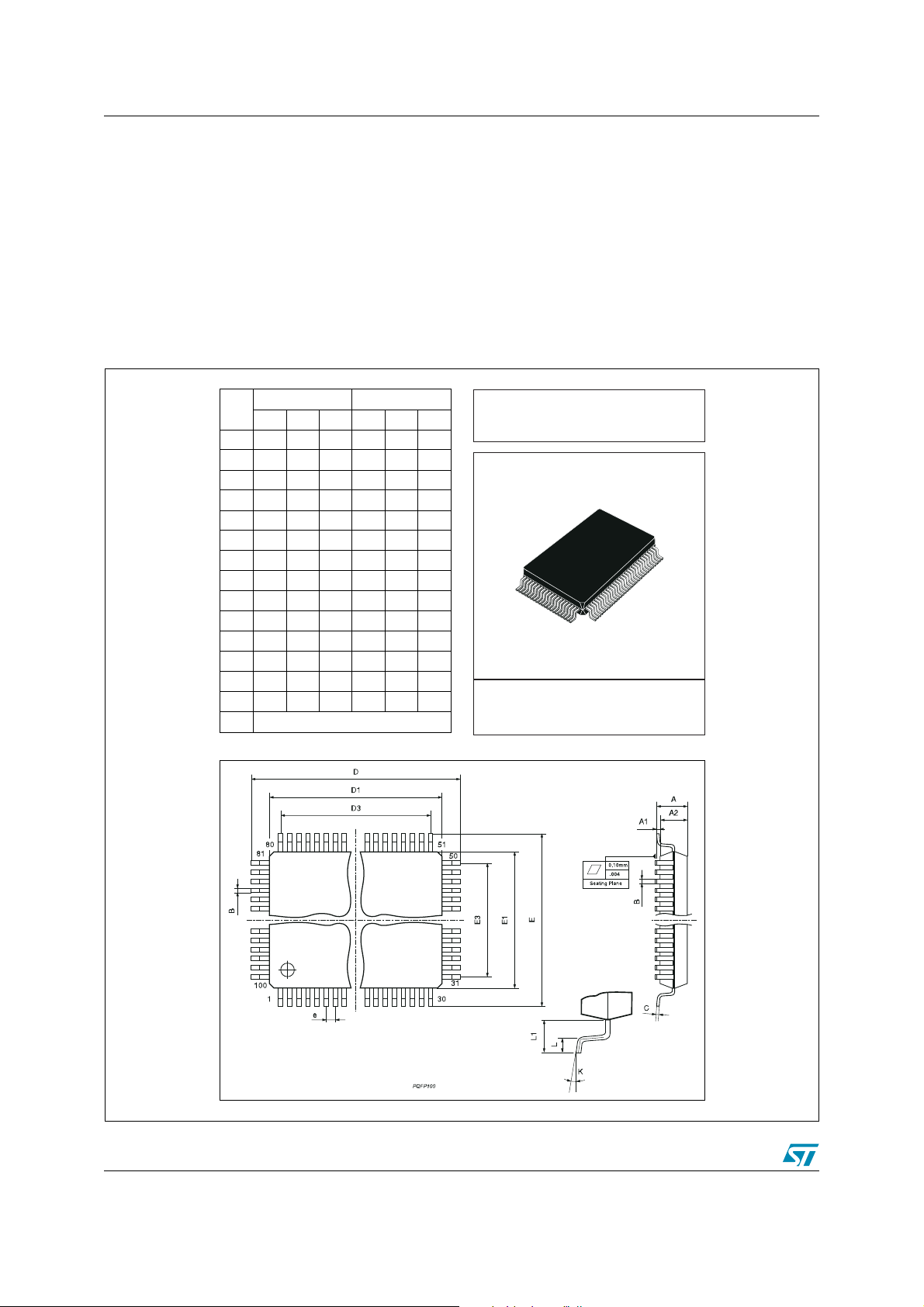
DIM.
mm inch
MIN. TYP. MAX. MIN. TYP. MAX.
A 3.40 0.134
A1 0.25 0.010
A2 2.55 2.80 3.05 0.100 0.110 0.120
B 0.22 0.38 0.0087 0.015
C 0.13 0.23 0.005 0.009
D 22.95 23.20 23.45 0.903 0.913 0.923
D1 19.90 20.00 20.10 0.783 0.787 0.791
D3 18.85 0.742
e 0.65 0.026
E 16.95 17.20 17.45 0.667 0.677 0.687
E1 13.90 14.00 14.10 0.547 0.551 0.555
E3 12.35 0.486
L 0.65 0.80 0.95 0.026 0.031 0.037
L1 1.60 0.063
K
0°
(min.), 7°(max.)
OUTLINE AND
MECHANICAL DATA
5 Package information
In order to meet environmental requirements, ST offers these devices in ECOPACK® packages.
These packages have a Lead-free second level interconnect. The category of second Level
Interconnect is marked on the package and on the inner box label, in compliance with JEDEC
Standard JESD97. The maximum ratings related to soldering conditions are also marked on
the inner box label.
ECOPACK is an ST trademark. ECOPACK specifications are available at: www.st.com.
Figure 16. PQFP100 Mechanical Data & Package Dimensions
20/22
Page 21

L6452 Revision history
6 Revision history
Date Revision Changes
15-Mar-1999 1 Initial release.
Modified Electrical Specification and any Time Diagrams.
Modified pin and signal names through out the spec.
06-Feb-2006 2
Modified Ta ble 1 Pin function pins 83, 84 & 86.
Added ESD parameter in the Ta ble 2 Absolute maximum ratings.
, T
Modified Ta ble 3 : T
Modified Figure 14.
set
hold
and R
parameters.
pon
21/22
Page 22

L6452
Please Read Carefully:
Information in this document is provided solely in connection with ST products. STMicroelectronics NV and its subsidiaries (“ST”) reserve the
right to make changes, corrections, modifications or improvements, to this document, and the products and services described herein at any
time, without notice.
All ST products are sold pursuant to ST’s terms and conditions of sale.
Purchasers are solely responsible for the choice, selection and use of the ST products and services described herein, and ST assumes no
liability whatsoever relating to the choice, selection or use of the ST products and services described herein.
No license, express or implied, by estoppel or otherwise, to any intellectual property rights is granted under this document. If any part of this
document refers to any third party products or services it shall not be deemed a license grant by ST for the use of such third party products
or services, or any intellectual property contained therein or considered as a warranty covering the use in any manner whatsoever of such
third party products or services or any intellectual property contained therein.
UNLESS OTHERWISE SET FORTH IN ST’S TERMS AND CONDITIONS OF SALE ST DISCLAIMS ANY EXPRESS OR IMPLIED
WARRANTY WITH RESPECT TO THE USE AND/OR SALE OF ST PRODUCTS INCLUDING WITHOUT LIMITATION IMPLIED
WARRANTIES OF MERCHANTABILITY, FITNESS FOR A PARTICULAR PURPOSE (AND THEIR EQUIVALENTS UNDER THE LAWS
OF ANY JURISDICTION), OR INFRINGEMENT OF ANY PATENT, COPYRIGHT OR OTHER INTELLECTUAL PROPERTY RIGHT.
UNLESS EXPRESSLY APPROVED IN WRITING BY AN AUTHORIZE REPRESENTATIVE OF ST, ST PRODUCTS ARE NOT DESIGNED,
AUTHORIZED OR WARRANTED FOR USE IN MILITARY, AIR CRAFT, SPACE, LIFE SAVING, OR LIFE SUSTAINING APPLICATIONS,
NOR IN PRODUCTS OR SYSTEMS, WHERE FAILURE OR MALFUNCTION MAY RESULT IN PERSONAL INJURY, DEATH, OR
SEVERE PROPERTY OR ENVIRONMENTAL DAMAGE.
Resale of ST products with provisions different from the statements and/or technical features set forth in this document shall immediately void
any warranty granted by ST for the ST product or service described herein and shall not create or extend in any manner whatsoever, any
liability of ST.
ST and the ST logo are trademarks or registered trademarks of ST in various countries.
Information in this document supersedes and replaces all information previously supplied.
The ST logo is a registered trademark of STMicroelectronics. All other names are the property of their respective owners.
© 2006 STMicroelectronics - All rights reserved
STMicroelectronics group of companies
Australia - Belgium - Brazil - Canada - China - Czech Republic - Finland - France - Germany - Hong Kong - India - Israel - Italy - Japan -
Malaysia - Malta - Morocco - Singapore - Spain - Sweden - Switzerland - United Kingdom - United States of America
www.st.com
22/22
 Loading...