

High-voltage high and low side driver
Features
■ High voltage rail up to 600V
■ dV/dt immunity ±50V/nsec in full temperature
range
■ Driver current capability:
– 400mA source,
– 650mA sink
■ Switching times 50/30 nsec rise/fall with 1nF
load
■ CMOS/TTL Schmitt trigger inputs with
hysteresis and pull down
■ Under voltage lock out on lower and upper
driving section
■ Internal bootstrap diode
■ Outputs in phase with inputs
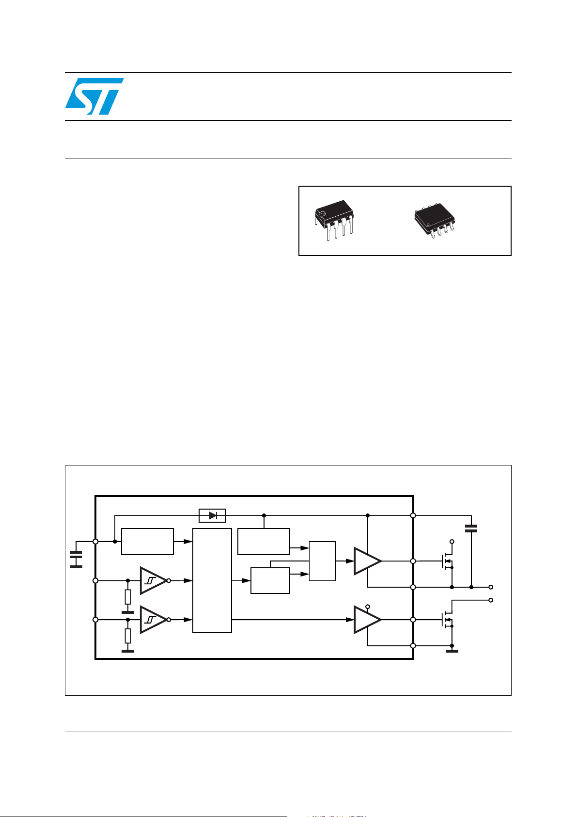
L6385E
DIP-8 SO-8
Description
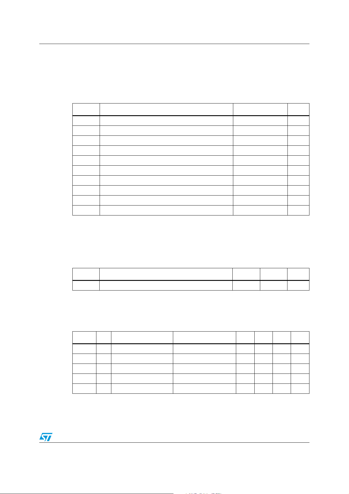
The L6385E is an high-voltage device,
manufactured with the BCD"OFF-LINE"
technology. It has an Half - Bridge Driver structure
that enables to drive independent referenced N
Channel Power MOS or IGBT. The High Side
(Floating) Section is enabled to work with voltage
Rail up to 600V. The Logic Inputs are CMOS/TTL
compatible for ease of interfacing with controlling
devices.
Figure 1. Block diagram
V
CC
HIN
LIN
3
2
1
UV
DETECTION
BOOTSTRAP DRIVER
LOGIC
UV
DETECTION
LEVEL
SHIFTER
R
R
S
LVG
DRIVER
V
CC
HVG
DRIVER
D97IN514B
Vboot
8
H.V.
HVG
7
OUT
6
LVG
5
GND
4
Cboot
TO LOAD
October 2007 Rev 1 1/16
www.st.com
16

Contents L6385E
Contents
1 Electrical data . . . . . . . . . . . . . . . . . . . . . . . . . . . . . . . . . . . . . . . . . . . . . . 3
1.1 Absolute maximum ratings . . . . . . . . . . . . . . . . . . . . . . . . . . . . . . . . . . . . . 3
1.2 Thermal data . . . . . . . . . . . . . . . . . . . . . . . . . . . . . . . . . . . . . . . . . . . . . . . 3
1.3 Recommended operating conditions . . . . . . . . . . . . . . . . . . . . . . . . . . . . . 3
2 Pin connection . . . . . . . . . . . . . . . . . . . . . . . . . . . . . . . . . . . . . . . . . . . . . . 4
3 Electrical characteristics . . . . . . . . . . . . . . . . . . . . . . . . . . . . . . . . . . . . . 5
3.1 AC operation . . . . . . . . . . . . . . . . . . . . . . . . . . . . . . . . . . . . . . . . . . . . . . . 5
3.2 DC operation . . . . . . . . . . . . . . . . . . . . . . . . . . . . . . . . . . . . . . . . . . . . . . . 5
3.3 Timing diagram . . . . . . . . . . . . . . . . . . . . . . . . . . . . . . . . . . . . . . . . . . . . . . 6
4 Bootstrap driver . . . . . . . . . . . . . . . . . . . . . . . . . . . . . . . . . . . . . . . . . . . . 7
4.1 CBOOT selection and charging . . . . . . . . . . . . . . . . . . . . . . . . . . . . . . . . . 7
5 Typical characteristic . . . . . . . . . . . . . . . . . . . . . . . . . . . . . . . . . . . . . . . . 9
6 Package mechanical data . . . . . . . . . . . . . . . . . . . . . . . . . . . . . . . . . . . . 12
7 Order codes . . . . . . . . . . . . . . . . . . . . . . . . . . . . . . . . . . . . . . . . . . . . . . . 15
8 Revision history . . . . . . . . . . . . . . . . . . . . . . . . . . . . . . . . . . . . . . . . . . . 16
2/16
L6385E Electrical data
1 Electrical data
1.1 Absolute maximum ratings
Table 1. Absolute maximum ratings
Symbol Parameter Value Unit
V
V
V
V
V
dV
P
T
Output voltage -3 to V
out
Supply voltage - 0.3 to +18 V
cc
Floating supply voltage -1 to 618 V
boot
High sidegate output voltage -1 to V
hvg
Low side gate output voltage -0.3 to Vcc +0.3 V
lvg
V
Logic input voltage -0.3 to Vcc +0.3 V
i
Allowed output slew rate 50 V/ns
out/dt
Total power dissipation (TJ = 85 °C) 750 mW
tot
Junction temperature 150 °C
T
j
Storage temperature -50 to 150 °C
s
boot
-18 V
V
boot
Note: ESD immunity for pins 6, 7 and 8 is guaranteed up to 900 V (Human Body Model)
1.2 Thermal data
Table 2. Thermal data
Symbol Parameter SO-8 DIP-8 Unit
R
Thermal Resistance Junction to ambient 150 100 °C/W
th(JA)
1.3 Recommended operating conditions
Table 3. Recommended operating conditions
Symbol Pin Parameter Test condition Min Typ Max Unit
V
out
V
BS
f
sw
V
cc
T
1. If the condition Vboot - Vout < 18V is guaranteed, Vout can range from -3 to 580V
2. VBS = V
6 Output voltage
(2)
8 Floating supply voltage
Switching frequency HVG,LVG load CL = 1nF 400 kHz
3 Supply voltage 17 V
J
Junction temperature -45 125 °C
- V
boot
out
3/16
(1)
(1)
17 V
580 V
Pin connection L6385E
2 Pin connection
Figure 2. Pin connection (Top view)
Table 4. Pin description
LIN
HIN
V
GND
1
2
3
CC
4 LVG
D97IN517A
V
8
boot
HVG
7
OUT
6
5
N° Pin Type Function
1 LIN I Low side driver logic input
2 HIN I High side driver logic input
3 V
Low voltage power supply
cc
4 GND Ground
5 LVG
(1)
O Low side driver output
6 VOUT O High side driver floating reference
7 HVG
8 V
1. The circuit guarantees 0.3V maximum on the pin (@ Isink = 10mA). This allows to omit the "bleeder"
resistor connected between the gate and the source of the external MOSFET normally used to hold the pin
low.
(1)
O High side driver output
Bootstrap supply voltage
boot
4/16
L6385E Electrical characteristics
3 Electrical characteristics
3.1 AC operation
Table 5. AC operation electrical characteristcs (VCC = 15V; TJ = 25°C)
Symbol Pin Parameter Test condition Min Typ Max Unit
1 vs 5
t
on
2 vs 7
1 vs 5
t
off
2 vs 7
t
r
t
f
High/low side driver turn-on
propagation delay
High/low side driver turn-off
propagation delay
5, 7 Rise time CL = 1000pF 50 ns
5, 7 Fall time CL = 1000pF 30 ns
3.2 DC operation
Table 6. DC operation electrical characteristcs (VCC = 15V; TJ = 25°C)
Symbol Pin Parameter Test condition Min Typ Max Unit
Low supply voltage section
V
V
V
I
V
cc
ccth1
ccth2
cchys
qccu
Supply voltage 17 V
Vcc UV turn on threshold 9.1 9.6 10.1 V
Vcc UV turn off threshold 7.9 8.3 8.8 V
Vcc UV hysteresis 1.3 V
3
Undervoltage quiescent
supply current
= 0V 110 ns
V
out
= 0V 105 ns
V
out
V
≤ 9V 150 220 µA
cc
Quiescent current Vin = 15V 250 320 µA
Bootstrap driver on
resistance
(1)
V
≥12.5V 125 Ω
cc
R
I
qcc
dson
Bootstrapped supply voltage section
V
BS
V
V
BSth1
V
V
BSth2
V
V
BShys
I
QBS
I
LK
Bootstrap supply voltage 17 V
UV turn on threshold 8.5 9.5 10.5 V
BS
UV turn off threshold 7.2 8.2 9.2 V
BS
8
UV hysteresis 1.3 V
BS
VBS quiescent current HVG ON 200 µA
= V
High voltage leakage current
V
V
hvg
boot
=
out
= 600V
10 µA
High/low side driver
I
so
Sink short circuit current VIN = Vil (tp < 10µs) 450 650 mA
I
si
Source short circuit current V
5,7
= Vih (tp < 10µs) 300 400 mA
IN
5/16
 Loading...