

查询L6384供应商
HIGH-VOLTAGEHALF BRIDGE DRIVER
HIGHVOLTAGERAIL UP TO 600 V
dV/dt IMMUNITY +- 50 V/nsec IN FULL TEM-
PERATURERANGE
DRIVER CURRENTCAPABILITY:
400 mASOURCE,
650 mASINK
SWITCHING TIMES 50/30 nsec RISE/FALL
WITH 1nF LOAD
CMOS/TTL SCHMITT TRIGGER INPUTS
WITH HYSTERESISANDPULL DOWN
SHUTDOWN INPUT
DEAD TIME SETTING
UNDERVOLTAGELOCKOUT
INTEGRATEDBOOTSTRAPDIODE
CLAMPINGON Vcc
SO8/MINIDIPPACKAGES
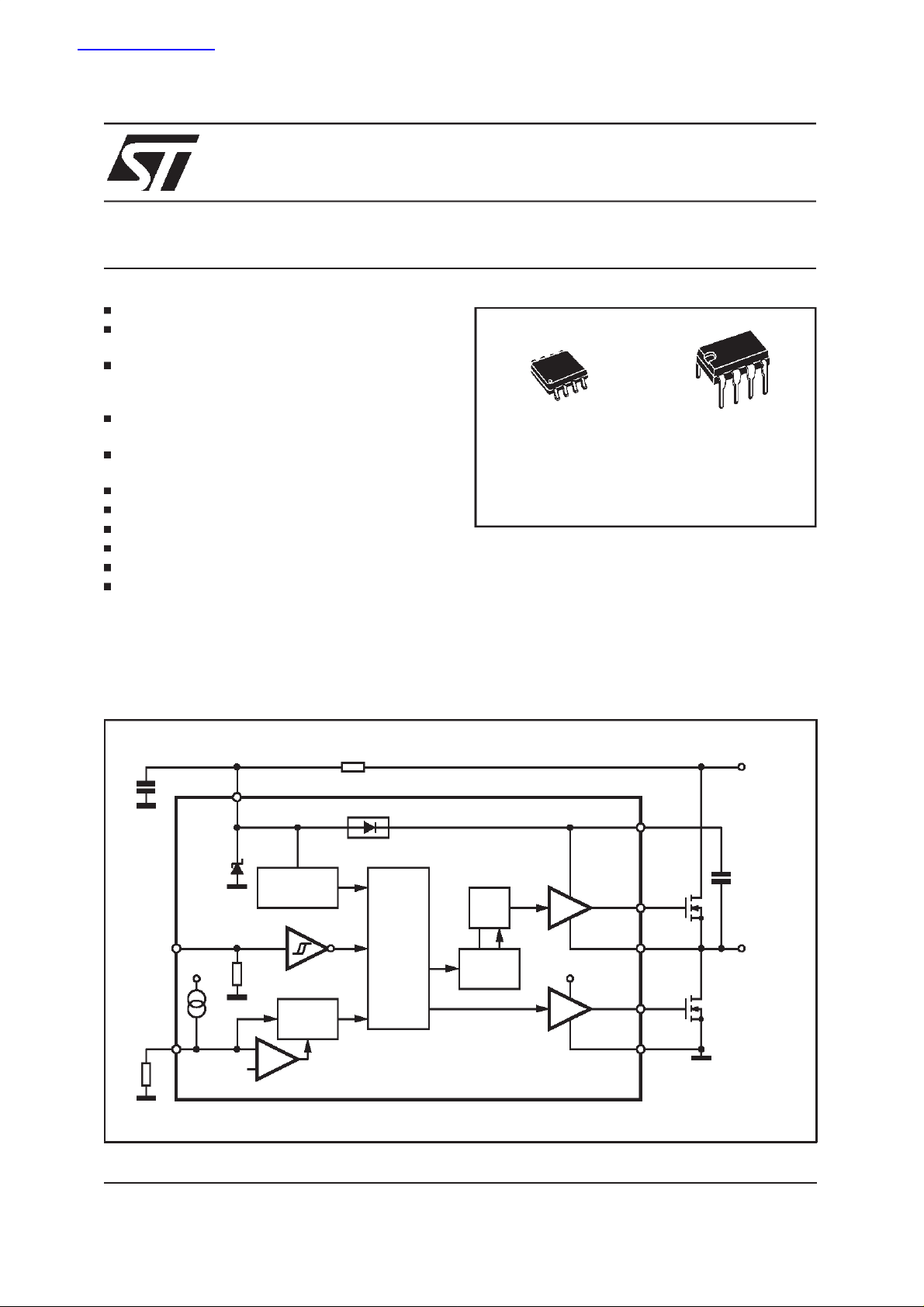
DESCRIPTION
The L6384 is an high-voltage device, manufactured with the BCD”OFF-LINE” technology.It has
L6384
SO8 Minidip
ORDERING NUMBERS:
L6384D L6384
an Half - Bridge Driver structure that enables to
drive N Channel PowerMOS or IGBT. The Upper
(Floating) Section is enabled to work with voltage
Rail up to 600V. TheLogic Inputs are CMOS/TTL
compatible for ease of interfacing with controlling
devices. Matched delays between Lower and Upper Section simplify high frequency operation.
Dead timesettingcan bereadily accomplishedby
means of an external resistor.
BLOCK DIAGRAM
V
CC
1
IN
V
CC
Idt
DT/SD
3
Vthi
2
DETECTION
BOOTSTRAP DRIVER
UV
DEAD
TIME
LOGIC
RS
LEVEL
SHIFTER
LVG
DRIVER
V
CC
HVG
DRIVER
H.V.
V
8
BOOT
C
BOOT
HVG
7
OUT
6
LVG
5
GND
4
D97IN518A
LOAD
May 2000
1/10
L6384
ABSOLUTE MAXIMUM RATINGS
Symbol Parameter Value Unit
Vout Output Voltage -3 toVboot -18 V
Vcc Supply Voltage(*) - 0.3 to 14.6 V
Is Supply Current(*) 25 mA
Vboot Floating Supply Voltage -1 to 618 V
Vhvg Upper Gate Output Voltage -1 to Vboot V
Vlvg Lower Gate Output Voltage -0.3 toVcc +0.3 V
Vi Logic Input Voltage -0.3 toVcc +0.3 V
Vsd Shut Down/Dead Time Voltage -0.3 toVcc +0.3 V
dVout/dt Allowed Output Slew Rate 50 V/ns
Ptot Total Power Dissipation (Tj = 85 °C) 750 mW
Tj Junction Temperature 150 °C
Ts Storage Temperature -50 to 150 °C
(*) The device has an internal Clamping Zenerbetween GND and the Vcc pin, It must not be supplied by a Low Impedence Voltage Source.
Note: ESD immunity for pins 6, 7 and 8 is guaranteedup to 900 V (HumanBody Model)
PIN CONNECTION
IN
V
CC
DT/SD
GND
1
2
3
4 LVG
D97IN519
V
8
7
6
BOOT
HVG
VOUT
5
THERMAL DATA
Symbol Parameter SO8 Minidip Unit
R
th j-amb
Thermal ResistanceJunction to Ambient 150 100 °C/W
PIN DESCRIPTION
N. Name Type Function
1 IN I Logic Input:it is in phase with HVG and in opposition of phase with LGV. It is compatible
2 Vcc I Supply input voltage: there is an internalclamp [Typ. 15.6V]
3 DT/SD I High impedance pin with two functionalities. When pulled lower than Vdt [Typ. 0.5V] the
4 GND Ground
to V
voltage. [Vil Max = 1.5V, Vih Min = 3.6V]
CC
device isshut down. A voltage higher than Vdt sets the dead time between high side gate
driver and low sidegate driver. The dead timevalue can be set forcing a certain voltage
level on the pin or connectinga resistor between pin 3 and ground.
Care must be taken to avoid below threshold spikes on pin 3 that can cause undesired
shut down of the IC. For this reason the connection of the components between pin 3 and
ground has to be as shortas possible. This pin can not be left floating for the same reason.
The pin has not be pulled through a low impedance to V
current source that feeds Rdt. The operative range is:Vdt....270K ⋅ Idt, that allows a dt
range of0.4 - 3.1µs.
, because of thedrop on the
CC
2/10
L6384
PIN DESCRIPTION
(continued)
N. Name Type Function
5 LVG O Low Side Driver Output: the output stage can deliver 400mA source and 650mA sink [Typ.
Values].
The circuitguarantees 0.3V max on the pin (@ I
= 10mA) with VCC> 3V andlower than
sink
the turnon threshold. This allows to omit the bleederresistor connected between the gate
and thesourceof the external mosfet normally used to hold the pin low; thegate driver
ensures lowimpedance also in SD conditions.
6 Vout O Upper Driver Floating Reference: layout care has to be taken to avoid below ground
spikes on this pin.
7 HVG O High Side Driver Output: the output stage can deliver 400mA sourceand 650mA sink
[Typ. Values].
The circuitgurantees 0.3V max between this pin and Vout (@ I
= 10mA) with VCC>3V
sink
and lowerthan the turn on threshold.This allows to omit the bleeder resistorconnected
between thegate and the source of the external mosfet normally used to hold the pin low;
the gatedriver ensures low impedance also in SD conditions.
8 Vboot Bootstrap Supply Voltage: it is the upper driverfloating supply. The bootstrapcapacitor
connected betweenthis pin and pin6 can be fed by an internal structure named ”bootstrap
driver” (a patentedstructure). This structure can replace the externalbootstrap diode.
RECOMMENDED OPERATINGCONDITIONS
Symbol Pin Parameter Test Condition Min. Typ. Max. Unit
Vout 6 Output Voltage Note1 580 V
Vboot -
Vout
fsw Switching Frequency HVG,LVGloadCL= 1nF 400 kHz
Vcc 2 Supply Voltage Vclamp V
T
Note 1: If the condition Vboot - Vout < 18V is guaranteed, Vout can range from -3 to 580V.
8 Floating Supply Voltage Note1 17 V
j
Junction Temperature -45 125 °C
ELECTRICALCHARACTERISTICS
AC Operation(V
Symbol Pin Parameter Test Condition Min. Typ. Max. Unit
ton 1 vs
5,7
tonsd 3 vs
5,7
toff 1 vs
5,7
tr 7,5 Rise Time CL = 1000pF 70 ns
tf 7,5 Fall Time CL = 1000pF 30 ns
= 14.4V;Tj = 25°C)
CC
High/Low SideDriver
Turn-On Propagation Delay
Vout = 0V
R
= 47kΩ
dt
200+dt ns
Shut Down Input Propagation Delay 220 280 ns
High/Low SideDriver
Turn-Off Propagation Delay
Vout = 0V
R
= 47k
dt
Vout = 0V
R
= 146kΩ
dt
Vout = 0V
R
= 270k
dt
Ω
250 300 ns
200 250 ns
170 200 ns
Ω
DC Operation(VCC= 14.4V;Tj = 25°C)
Supply Voltage Section
Vclamp 2 Supply VoltageClamping Is =5mA 14.6 15.6 16.6 V
Vccth1 2 Vcc UV Turn On Threshold 11.5 12 12.5 V
Vccth2 2 Vcc UV Turn Off Threshold 9.5 10 10.5 V
3/10
 Loading...