

Features
■ Integrated high-voltage start-up
■ 4 drivers for PFC, half-bridge & pre-heating
MOSFETs
■ Fully integrated power management for all
operating modes
■ 5V microcontroller compatible
■ Internal two point V
■ Over-current protection with digital output
regulator
CC
signal
■ Cross-conduction protection (interlocking)
■ Under voltage lock-out
■ Integrated bootstrap diode
Applications
■ Dimmable / non-dimmable ballast
Figure 1. Block diagram
L6382D5
Power management unit
for microcontrolled ballast
SO-20
Description
The L6382D5 is suitable for microcontrolled
electronic ballasts embedding a PFC stage and a
half-bridge stage. The L6382D5 includes 4
MOSFET driving stages (for the PFC, for the half
bridge, for the preheating MOSFET) plus a power
management unit (PMU) featuring also a
reference able to supply the microcontroller in any
condition.
Besides increasing the application efficiency, the
L6382D5 reduces the bill of materials because
different tasks (regarding drivers and power
management) are performed by a single IC, which
improves the application reliability.
March 2007 Rev 3 1/21
www.st.com
21

Contents L6382D5
Contents
1 Device description . . . . . . . . . . . . . . . . . . . . . . . . . . . . . . . . . . . . . . . . . . 3
2 Pin settings . . . . . . . . . . . . . . . . . . . . . . . . . . . . . . . . . . . . . . . . . . . . . . . . 4
2.1 Pin connection . . . . . . . . . . . . . . . . . . . . . . . . . . . . . . . . . . . . . . . . . . . . . . 4
2.2 Pin description . . . . . . . . . . . . . . . . . . . . . . . . . . . . . . . . . . . . . . . . . . . . . . 4
3 Maximum ratings . . . . . . . . . . . . . . . . . . . . . . . . . . . . . . . . . . . . . . . . . . . . 6
3.1 Absolute maximum ratings . . . . . . . . . . . . . . . . . . . . . . . . . . . . . . . . . . . . . 6
3.2 Thermal data . . . . . . . . . . . . . . . . . . . . . . . . . . . . . . . . . . . . . . . . . . . . . . . 6
4 Electrical characteristics . . . . . . . . . . . . . . . . . . . . . . . . . . . . . . . . . . . . . 7
5 Application information . . . . . . . . . . . . . . . . . . . . . . . . . . . . . . . . . . . . . 11
5.1 Power management . . . . . . . . . . . . . . . . . . . . . . . . . . . . . . . . . . . . . . . . . 11
5.2 START-UP mode . . . . . . . . . . . . . . . . . . . . . . . . . . . . . . . . . . . . . . . . . . . 11
5.2.1 SAVE Mode . . . . . . . . . . . . . . . . . . . . . . . . . . . . . . . . . . . . . . . . . . . . . . 12
5.2.2 OPERATING Mode . . . . . . . . . . . . . . . . . . . . . . . . . . . . . . . . . . . . . . . . 12
5.2.3 Shut Down . . . . . . . . . . . . . . . . . . . . . . . . . . . . . . . . . . . . . . . . . . . . . . . 12
6 Block description . . . . . . . . . . . . . . . . . . . . . . . . . . . . . . . . . . . . . . . . . . 15
6.1 Supply section . . . . . . . . . . . . . . . . . . . . . . . . . . . . . . . . . . . . . . . . . . . . . 15
6.2 5V reference voltage . . . . . . . . . . . . . . . . . . . . . . . . . . . . . . . . . . . . . . . . 15
6.3 Drivers . . . . . . . . . . . . . . . . . . . . . . . . . . . . . . . . . . . . . . . . . . . . . . . . . . . 16
6.4 Internal logic, over current protection (OCP) and interlocking function . . 16
7 Package mechanical data . . . . . . . . . . . . . . . . . . . . . . . . . . . . . . . . . . . . 17
8 Order codes . . . . . . . . . . . . . . . . . . . . . . . . . . . . . . . . . . . . . . . . . . . . . . . 19
9 Revision history . . . . . . . . . . . . . . . . . . . . . . . . . . . . . . . . . . . . . . . . . . . 20
2/21
L6382D5 Device description
1 Device description
Designed in High-voltage BCD Off-line technology, the L6382D5 is provided with 4 inputs
pin and a high voltage start-up generator conceived for applications managed by a
microcontroller. It allows the designer to use the same ballast circuit for different lamp
wattage/type by simply changing the µC software.
The digital input pins - able to receive signals up to 400KHz - are connected to level shifters
that provide the control signals to their relevant drivers; in particular the L6382D5 embeds
one driver for the PFC pre-regulator stage, two drivers for the ballast half-bridge stage (High
Voltage, including also the bootstrap function) and the last one to provide supplementary
features like preheating of filaments supplied through isolated filaments in dimmable
applications.
A precise reference voltage (+5V ±2%) able to provide up to 30mA is available to supply the
µC in operating
is up to 10mA and it is provided by the internal high voltage start-up generator.
The chip has been conceived with advanced power management logic to minimize power
losses and increase the application reliability.
In the half-bridge section, a patented integrated bootstrap section replaces the external
bootstrap diode.
mode. Instead, during start-up and save mode the current available at V
REF
The L6382D5 integrates also a function that regulates the IC supply voltage (without the
need of any external charge pump) and optimizes the current consumption.
Figure 2. Typical system block diagram
3/21
Pin settings L6382D5
2 Pin settings
2.1 Pin connection
Figure 3. Pin connection (top view)
2.2 Pin description
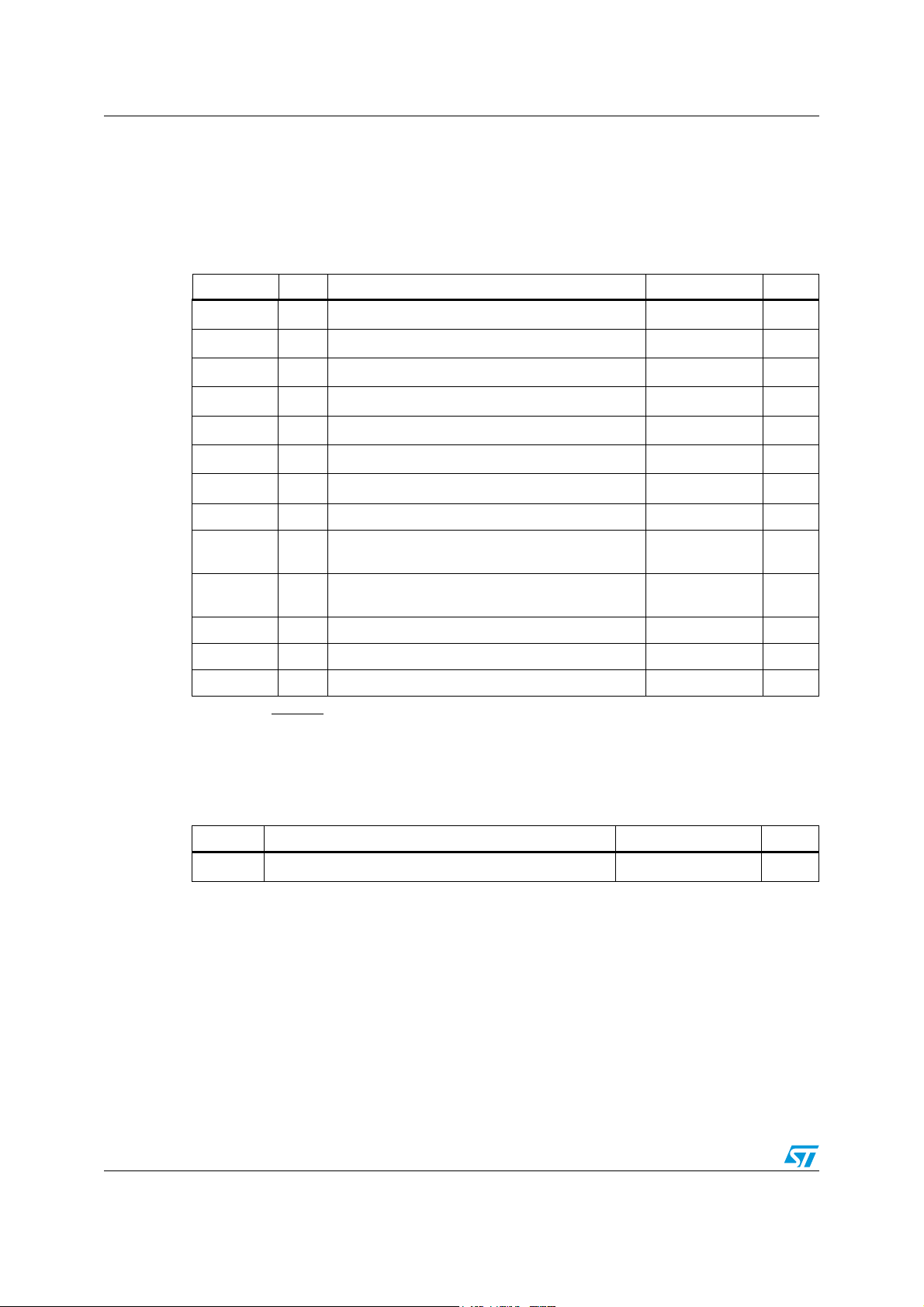
Table 1. Pin description
Name Pin N° Description
1PFI
2LSI
3HSI
Digital input signal to control the PFC gate driver. This pin has to be connected
to a 5V CMOS compatible signal.
Digital input signal to control the half-bridge low side driver. This pin has to be
connected to a 5V CMOS compatible signal.
Digital input signal to control the half-bridge high side driver. This pin has to be
connected to a 5V CMOS compatible signal.
PFI
PFI
LSI
LSI
HSI
HSI
HEI
HEI
PFG
PFG
N.C.
N.C.
TPR
TPR
GND
GND
LSG
LSG
VCC
VCC
1
1
2
2
3
3
4
4
5
5
6
6
7
7
8
8
9
9
10
10
20
20
19
19
18
18
17
17
16
16
15
15
14
14
13
13
12
12
11
11
VREF
VREF
CSI
CSI
CSO
CSO
HEG
HEG
N.C.
N.C.
HVSU
HVSU
N.C.
N.C.
OUT
OUT
HSG
HSG
BOOT
BOOT
4HEI
5PFG
6 N.C. Not connected
7TPR
8GND
4/21
Digital input signal to control the HEG output. This pin has to be connected to a
5V CMOS compatible signal.
PFC Driver Output. This pin must be connected to the PFC power MOSFET
gate. A resistor connected between this pin and the power MOS gate can be
used to reduce the peak current. An internal 10KΩ resistor toward ground
avoids spurious and undesired MOSFET turn-on
The totem pole output stage is able to drive the power MOS with a peak
current of 120mA source and 250mA sink.
Input for two point regulator; by coupling the pin with a capacitor to a switching
circuit, it is possible to implement a charge circuit for the Vcc.
Chip ground. Current return for both the low-side gate-drive currents and the
bias current of the IC. All of the ground connections of the bias components
should be tied to a track going to this pin and kept separate from any pulsed
current return.
L6382D5 Pin settings
Table 1. Pin description (continued)
Name Pin N° Description
Low Side Driver Output. This pin must be connected to the gate of the halfbridge low side power MOSFET. A resistor connected between this pin and the
power MOS gate can be used to reduce the peak current.
9LSG
10 Vcc Supply Voltage for the signal part of the IC and for the drivers.
11 BOOT
12 HSG
13 OUT
14 N.C. Not connected
An internal 20KΩ resistor toward ground avoids spurious and undesired
MOSFET turn-on.
The totem pole output stage is able to drive power with a peak current of
120mA source and 120mA sink.
High-side gate-drive floating supply Voltage. The bootstrap capacitor
connected between this pin and pin 13 (OUT) is fed by an internal
synchronous bootstrap diode driven in phase with the low-side gate-drive. This
patented structure normally replaces the external diode.
High Side Driver Output. This pin must be connected to the gate of the half
bridge high side power MOSFET . A resistor connected between this pin and
the power MOS gate can be used to reduce the peak current.
An internal 20KΩ resistor toward OUT pin avoids spurious and undesired
MOSFET turn-on
The totem pole output stage is able to drive the power MOS with a peak
current of 120mA source and 120mA sink.
High-side gate-drive floating ground. Current return for the high-side gate-drive
current. Layout carefully the connection of this pin to avoid too large spikes
below ground.
15 HVSU
16 N.C.
17 HEG
18 CSO
19 CSI
20 VREF
High-voltage start-up. The current flowing into this pin charges the capacitor
connected between pin Vcc and GND to start up the IC. Whilst the chip is in
mode, the generator is cycled on-off between turn-on and save mode
save
voltages. When the chip works in operating
and it is re-enabled when the Vcc voltage falls below the UVLO threshold.
According to the required V
rectified mains voltage either directly or through a resistor.
High-voltage spacer. The pin is not connected internally to isolate the highvoltage pin and comply with safety regulations (creepage distance) on the
PCB.
Output for the HEI block; this driver can be used to drive the MOS employed in
isolated filaments preheating. An internal 20KΩ resistor toward ground avoids
spurious and undesired MOSFET turn-on.
Output of current sense comparator, compatible with 5V CMOS logic; during
operating
triggered (CSI> 0.55 typ.) the pin latches high.
Input of current sense comparator, it is enabled only during operating
when the pin voltage exceeds the internal threshold, the CSO pin is forced
high and the half bridge drivers are disabled. It exits from this condition by
either cycling the Vcc below the UVLO or with LGI=HGI=low simultaneously.
Voltage reference. During operating
accurate voltage reference that can be used to supply up to 30mA to an
external circuit. A small film capacitor (0.22µF min.), connected between this
pin and GND is recommended to ensure the stability of the generator and to
prevent noise from affecting the reference.
mode, the pin is forced low whereas whenever the OC comparator is
pin current, this pin can be connected to the
REF
mode the generator is shut down
mode;
mode an internal generator provides an
5/21
Maximum ratings L6382D5
3 Maximum ratings
3.1 Absolute maximum ratings
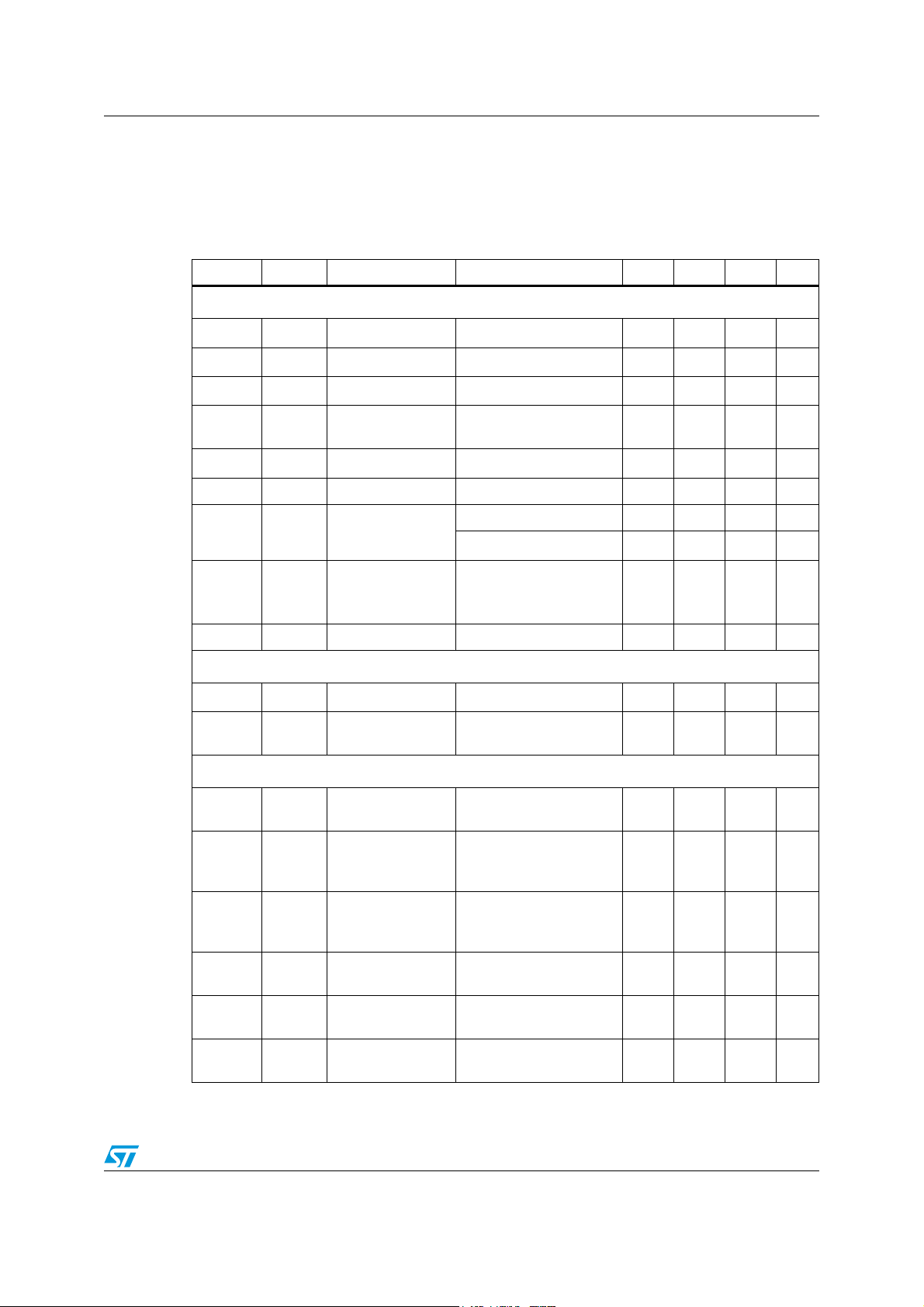
Table 2. Absolute maximum ratings
Symbol Pin Parameter Value Unit
V
CC
V
HVSU
V
BOOT
V
OUT
I
TPR(RMS)
I
TPR(PK)
V
TPR
10 IC supply voltage (ICC = 20mA) Self-limited
15 High voltage start-up generator voltage range -0.3 to 600 V
11 Floating supply voltage -1 to V
13 Floating ground voltage -1 to 600 V
7 Maximum TPR RMS current ±200 mA
7 Maximum TPR peak current ±600 mA
7
Maximum TPR voltage
19 CSI input voltage -0.3 to 7 V
1, 2,
Logic input voltage -0.3 to 7 V
3, 4
9, 12, 17Operating frequency 15 to 400 KHz
(1)
HVSU+VCC
14 V
V
5 Operating frequency 15 to 600 KHz
Tstg Storage Temperature -40 to +150 °C
Tj Ambient Temperature operating range -40 to +125 °C
1. Excluding operating mode
3.2 Thermal data
Table 3. Thermal data
Symbol Parameter Value Unit
R
thJA
Maximum thermal resistance junction-ambient 120 °C/W
6/21
L6382D5 Electrical characteristics
4 Electrical characteristics
Table 4. Electrical characteristcs (TJ = 25°C, VCC = 13V, C
unless otherwise specified)
DRIVER
= 1nF
Symbol Pin Parameter Test condition Min Typ Max Unit
Supply voltage
V
ccON
V
ccOFF
V
ccSM
VSMhys 10
V
REF(OFF)
10 Turn-on voltage 13 14 15 V
10 Turn-off voltage 8.5 9 9.5 V
10 Save mode voltage 12.75 13.8 14.85 V
Save mode
hysteresys
0.12 0.16 0.2 V
10 Reference turn-off 6 6.4 6.8 V
IvccON 10 Start-up current 160 µA
IvccSM 10
Ivcc 10
Save Mode current
consumption
Quiescent current
in operating mode
(1)
=13V;
V
CC
LGI = HGI = high;
no load on VREF.
190 250 µA
220 µA
2.1 mA
Vz 10 Internal Zener 16.5 17 18 V
High voltage start-up
IMSS 15 Maximum current
ILSS 15
Leakage current off
state
Two point regulator (TPR) protection
T
PR
st
PR
T
(ON)
T
PR
(OFF)
Vcc Protection
10
level
10 Vcc Turn-on level
10 Vcc Turn-off level
Output voltage on
7
state
Forward voltage
7
drop Diode
Leakage current off
7
state
> 50V
V
HVSU
V
HVSU
= 600V
20 mA
40 µA
Operating mode 14.0 14.5 15.0 V
Operating mode; after
the first falling edge on
12.5 13 13.5 V
LSG
Operating mode; after
the first falling edge on
12.45 12.95 13.48 V
LSG
I
= 200mA
TPR
@ 600mA forward
current.
= 13V
V
TPR
2V
2.3 V
5µA
7/21

Electrical characteristics L6382D5
Table 4. Electrical characteristcs (TJ = 25°C, VCC = 13V, C
unless otherwise specified)
(continued)
DRIVER
= 1nF
Symbol Pin Parameter Test condition Min Typ Max Unit
LSG, HEG & PFG drivers
V
OH(LS
V
OL(LS)
5, 9
)
5, 9
HIGH Output
Voltage
17 IHEG = 2.5mA
LOW Output
Voltage
17 IHEG = 2.5mA
Source Current
Capability
ILSG = IPFG = 10mA
12.5 V
ILSG = IPFG = 10mA
0.5 V
LSG and PFG 120 mA
HEG 50 mA
LSG 120 mA
Sink Current
Capability
HEG 70
PFG 250
T
RISE
5
Rise time Cload = 1nF
80
17 60
T
FAL L
5,
Fall time Cload = 1nF
60
17 40
LSG; high to low and low
to high
300 ns
ns 9300
ns9110
T
DELAY
R
B
Propagation delay
(input to output)
Pull down Resistor
HSG driver (voltages referred to OUT)
V
OH(HS)
V
OL(HS)
T
RISE
HIGH Output
12
Voltage
LOW Output
12
Voltage
Sink Current
12
Capability
Source Current
12
Capability
12 Rise time Cload = 1nF 115 ns
HEG; high to low and low
to high
200 ns
PFG; high to low 250 ns
PFG; low to high 200 ns
LSG 20 KΩ
HEG 50 KΩ
PFG 10 KΩ
IHSG = 10 mA 12.5 V
IHSG = 10 mA 0.5 V
120 mA
120 mA
8/21

L6382D5 Electrical characteristics
Table 4. Electrical characteristcs (TJ = 25°C, VCC = 13V, C
unless otherwise specified)
(continued)
DRIVER
= 1nF
Symbol Pin Parameter Test condition Min Typ Max Unit
T
FAL L
T
DELAY
R
B
12 Fall time Cload = 1nF 75 ns
Propagation delay
12
(LGI to LSG)
high to low and low to
high
300 ns
12 Pull down Resistor to OUT 20 KΩ
High-side floating gate-driver supply
I
LKBOOT
I
LKOUT
11
current
OUT pin leakage
13
current
BOOT
V
BOOT
V
OUT
= 580V
= 562V
5µA
5µA
V
pin leakage
Synchronous
R
DS(on)
bootstrap
diode on-
V
LVG
= HIGH
150 Ω
resistance
Forward Voltage
Drop
Forward Current
at 10 mA forward current 2.4 V
at 5V forward voltage
drop
20 mA
V
REF
V
REF
20 Reference voltage 15mA load. 4.9 5 5.1 V
20 Load regulation IRef = -3 to +30 mA -20 2 mV
20 Voltage change
V
REF
protection
V
REF
@3mA
Current Drive
Capability
I
REF
20
20
20
Overcurrent buffer stage
V
CSI
I
CSI
19 Comparator Level 0.52 0.54 0.56 V
19 Input Bias Current 500 nA
Propagation delay CSO turn off to LSG low 200 ns
latched
Clamp
15mA load; Vcc = 9V to
15V
15 mV
3.2 V
V
from 0 to V
CC
during start-up; Vcc from
V
REF(OFF)
shut-down; V
to 0 during
REF
CCON
< 2V
1.2 1.8 V
-3 +30 mA
Save mode -3 +10 mA
9/21

Electrical characteristics L6382D5
Table 4. Electrical characteristcs (TJ = 25°C, VCC = 13V, C
unless otherwise specified)
(continued)
DRIVER
= 1nF
Symbol Pin Parameter Test condition Min Typ Max Unit
V
-
18 High output voltage
18 Low output voltage
I
CSO
I
CSO
= 200µA
= -150µA
REF
0.5V
0.5 V
DIM
Normal Mode Time
Out
Vref enabling
drivers
T
ED
Time enabling
drivers
65 100 135 µs
4.6 V
10 µs
Logic input
1 to 4
1 to 4
Low Level Logic
Input Voltage
High Level Logic
Input Voltage
1.3 V
3.7 V
LGI Pull down resistor 100 KΩ
1. Specification over the -40°C to +125°C junction temperature range are ensured by design, characterization
and statistical correlation.
10/21

L6382D5 Application information
5 Application information
5.1 Power management
The L6382D5 has two stable states (save mode and operating mode) and two additional
states that manage the Start-up and fault conditions: the Over Current Protection is a
parallel asynchronous process enabled when in operating
Following paragraphs will describe each mode and the condition necessary to shift between
them.
Figure 4. State diagram
mode Figure 4.
VCC>V
CC(ON)
V
>4.6V
REF
&
>10µs
T
DE
5.2 START-UP mode
With reference to the timing diagram of figure 6, when power is first applied to the converter,
the voltage on the bulk capacitor (Vin) builds up and the HV generator is enabled to operate
drawing about 10mA. This current, diminished by the IC consumption (less than 150µA),
charges the bypass capacitor connected between pin Vcc and ground and makes its voltage
rise almost linear.
START-UP
VCC<V
SAVE MODE
OPERATING
MODE
REF(OFF)
LGI low
for more
than 100µs
V
CC<VCC(ON)
VCC<V
V
REF(OFF)
SHUT DOWN
< V
CC
CC(OFF)
or
V
<3.2V
REF
During this phase, all IC's functions are disabled except for:
● the current sinking circuit on V
pin that maintains low the voltage by keeping
REF
disabled the microcontroller connected to this pin;
● the High-Voltage Start-Up (HVSU) that is ON (conductive) to charge the external
capacitor on pin Vcc.
As the Vcc voltage reaches the start-up threshold (14V typ.) the chip starts operating and
the HV generator is switched off.
11/21

Application information L6382D5
Summarizing:
– The high-voltage start-up generator is active;
–V
is disabled with additional sinking circuit on pin V
REF
REF
enabled;
– TPR is disabled;
– OCP is disabled;
– The drivers are disabled.
5.2.1 SAVE Mode
This mode is entered after the VCC voltage reaches the turn-on threshold; the VREF is
enabled in low current source mode to supply the µC connected to it, whose wake-up
required current must be less than 10mA: if no switching activity is detected at LGI input, the
high voltage start-up generator cycles ON-OFF keeping the Vcc voltage between VccON
and V
Summarizing:
.
ccSM
– The high-voltage start-up generator is cycling;
–V
is enabled in low source current capability (I
REF
– TPR circuit is disabled;
– OCP is disabled;
– The drivers are disabled.
≤ 10mA);
REF
If the V
voltage falls below the V
CC
5.2.2 OPERATING Mode
After 10µs in save mode and only if the votage at V
edge on the HGI input, the driver are enabled as well as all the IC's functions; this is the
mode correspondent to the proper lamp behaviour.
Summarizing:
– HVSU is OFF
–V
is enabled in high source current mode (I
REF
– TPR circuit is enabled
– OCP is enabled
– The drivers are enabled
If there is no switching activity on LGI for more than 100µs, the IC returns in save
5.2.3 Shut Down
This state permits to manage the fault conditions in operating mode and it is entered by the
occurrence on one of the following conditions:
1. V
2. V
< V
CC
< 3.2V (Under Voltage fault on V
REF
(Under Voltage fault on Supply),
ccOff
REF(OFF)
threshold, the device enters the start-up mode.
is higher than 4.6V, on the falling
REF
< 30mA)
REF
mode.
)
REF
12/21

L6382D5 Application information
In this state the functions are:
– The HVSU generator is ON
–V
is enabled in low source current mode (I
REF
< 10mA)
REF
–TPR is disabled
– OCP is disabled
– The drivers are disabled
In this state if Vcc reaches V
V
CC
< V
REF(OFF)
, also the µC is turned off and the device will be ready to execute the Start-
, the device enters the save mode otherwise, if
ccOn
up sequence.
Figure 5. Timing Sequences, TPR behavior
13/21

Application information L6382D5
Figure 6. Timing Sequences, save mode and operating mode
14/21

L6382D5 Block description
6 Block description
6.1 Supply section
● µPUVLO ( Power Under Voltage Lock Out): This block controls the power
management of the L6382D5 ensuring the right current consumption in each operating
state, the correct V
up generator switching.
During Start-up the device sinks the current necessary to charge the external capacitor
on pin V
from the high voltage bus; in this state the other IC's functions are disabled
CC
and the current consumption of the whole IC is less than 150µA.
When the voltage on V
µPUVLO block controls Vcc between VccON and VccSM by switching ON/OFF the
high voltage start-up generator.
● HVSU (High-Voltage Start-Up generator): a 600V internal MOS transistor structure
controls the Vcc supply voltage during START UP and SAVE MODE conditions and it
reduces the power losses during operating MODE by switching off the MOS transistor.
The transistor has a source current capability of up to 30mA.
● TPR (Two Point Regulator) & PWS: during operating mode, the TPR block controls
the PSW switch in order to regulate the IC supply voltage (V
between TPR(ON) and TPR(OFF) by switching ON and OFF the PSW transistor.
– Vcc > TPRst: the PSW is switched ON immediately;
– TPR(ON) < Vcc < TPRst: the PSW is switched ON at the following falling edge of
LGI;
– Vcc < TPR(OFF): the PSW is switched OFF at the following falling edge on LGI.
current capability, the driver enabling and the high-voltage start-
REF
pin reaches VccON, the IC enters the save mode where the
CC
) to a value in the range
CC
When the PSW switch is OFF, the diodes build a charge pump structure so that, connecting
the TPR pin to a switching voltage (through a capacitor) it is possible to supply the low
voltage section of the chip without adding any further external component. The diodes and
the switch are designed to withstand a peak current of at least 200mA
6.2 5V reference voltage
This block is used to supply the microcontroller; this source is able to supply 10mA in save
mode and 30mA in normal mode; moreover, during start-up
an additional circuit is ensures that, even sinking 3mA, the pin voltage doesn't exceed 1.2V.
The reference is available until Vcc is above V
additional sinking circuit is enabled again.
REF(OFF)
.
RMS
when V
is not yet available,
REF
; below that it turns off and the
15/21

Block description L6382D5
6.3 Drivers
● LSD (Low Side Driver): it consists of a level shifter from 5V logic signal (LSI) to Vcc
MOS driving level; conceived for the half-bridge low-side power MOS, it is able to
source and sink 120mA (min).
● HSD (Level Shifter and High Side Driver): it consists of a level shifter from 5V logic
signal (HSI) to the high side gate driver input up to 600V. Conceived for the half-bridge
high-side power MOS, the HSD is able to source and sink 120mA.
● PFD (Power Factor Driver): it consists of a level shifter from 5V logic signal (PFI) to Vcc
MOS driving level: the driver is able to source 120mA from V
sink 250mA to GND (turn-off); it is suitable to drive the MOS of the PFC pre-regulator
stage.
● HED (Heat Driver): it consists of a level shifter from 5V logic signal (HEI) to Vcc MOS
driving level; the driver is able to source 30mA from Vcc to HEG and to sink 75mA to
GND and it is suitable for the filament heating when they are supplied by independent
winding.
● Bootstrap Circuit: it generates the supply voltage for the high side Driver (HSD). This
circuit sources current from V
to PIN HSB when LSG in ON. A patented integrated
CC
bootstrap section replaces an external bootstrap diode. This section together with a
bootstrap capacitor provides the bootstrap voltage to drive the high side power
MOSFET. This function is achieved using a high voltage DMOS driver which is driven
synchronously with the low side external power MOSFET. For a safe operation, current
flow between BOOT pin and Vcc is always inhibited, even though ZVS operation may
not be ensured.
to PFG (turn-on) and to
CC
6.4 Internal logic, over current protection (OCP) and interlocking function
The DIM (Digital Input Monitor) block manages the input signals delivered to the drivers
ensuring that they are low during the described start-up procedure; the DIM block controls
the L6382D5 behaviour during both save
When the voltage on pin CSI overcomes the internal reference of 0.54V (typ.) the block
latches the fault condition: in this state the OCP block forces low both HSG and LSG signals
while CSO will be forced high. This condition remains latched until LSI and HSI are
simultaneously low and CSI is below 0.54V.
This function is suitable to implement an over current protection or hard-switching detection
by using an external sense resistor.
As the voltage on pin CSI can go negative, the current must be limited below 2mA by
external components.
Another feature of the DIM block is the internal interlocking that avoids cross-conduction in
the half-bridge FET's: if by chance both HSI and LSI input's are brought high at the same
time, then LSG and HSG are forced low as long as this critical condition persists.
and operating modes.
16/21

L6382D5 Package mechanical data
7 Package mechanical data
In order to meet environmental requirements, ST offers these devices in ECOPACK®
packages. These packages have a Lead-free second level interconnect . The category of
second level interconnect is marked on the package and on the inner box label, in
compliance with JEDEC Standard JESD97. The maximum ratings related to soldering
conditions are also marked on the inner box label. ECOPACK is an ST trademark.
ECOPACK specifications are available at: www.st.com
17/21

Package mechanical data L6382D5
Table 5. SO-20 Mechanical data
Dim.
mm. inch
Min Typ Max Min Typ Max
A 2.35 2.65 0.093 0.104
A1 0.10 0.30 0.004 0.012
B 0.33 0.51 0.013 0.200
C 0.23 0.32 0.009 0.013
D (1)
12.60 13.00 0.496 0.512
E 7.40 7.60 0.291 0.299
e 1.27 0.050
H 10.0 10.65 0.394 0.419
h 0.25 0.75 0.010 0.030
L 0.40 1.27 0.016 0.050
k 0° (min.), 8° (max.)
ddd 0.10 0.004
Figure 7. Package dimensions
18/21

L6382D5 Order codes
8 Order codes
Table 6. Order codes
Part number Package Packaging
L6382D5 SO-20 Tube
L6382D5TR SO-20 Tape & Reel
19/21

Revision history L6382D5
9 Revision history
Table 7. Revision history
Date Revision Changes
15-Jan-2004 1 First Issue
17-May-2006 2 Document reformatted
22-Mar-2007 3 Typo on Ta b le 2
20/21

L6382D5
Please Read Carefully:
Information in this document is provided solely in connection with ST products. STMicroelectronics NV and its subsidiaries (“ST”) reserve the
right to make changes, corrections, modifications or improvements, to this document, and the products and services described herein at any
time, without notice.
All ST products are sold pursuant to ST’s terms and conditions of sale.
Purchasers are solely responsible for the choice, selection and use of the ST products and services described herein, and ST assumes no
liability whatsoever relating to the choice, selection or use of the ST products and services described herein.
No license, express or implied, by estoppel or otherwise, to any intellectual property rights is granted under this document. If any part of this
document refers to any third party products or services it shall not be deemed a license grant by ST for the use of such third party products
or services, or any intellectual property contained therein or considered as a warranty covering the use in any manner whatsoever of such
third party products or services or any intellectual property contained therein.
UNLESS OTHERWISE SET FORTH IN ST’S TERMS AND CONDITIONS OF SALE ST DISCLAIMS ANY EXPRESS OR IMPLIED
WARRANTY WITH RESPECT TO THE USE AND/OR SALE OF ST PRODUCTS INCLUDING WITHOUT LIMITATION IMPLIED
WARRANTIES OF MERCHANTABILITY, FITNESS FOR A PARTICULAR PURPOSE (AND THEIR EQUIVALENTS UNDER THE LAWS
OF ANY JURISDICTION), OR INFRINGEMENT OF ANY PATENT, COPYRIGHT OR OTHER INTELLECTUAL PROPERTY RIGHT.
UNLESS EXPRESSLY APPROVED IN WRITING BY AN AUTHORIZED ST REPRESENTATIVE, ST PRODUCTS ARE NOT
RECOMMENDED, AUTHORIZED OR WARRANTED FOR USE IN MILITARY, AIR CRAFT, SPACE, LIFE SAVING, OR LIFE SUSTAINING
APPLICATIONS, NOR IN PRODUCTS OR SYSTEMS WHERE FAILURE OR MALFUNCTION MAY RESULT IN PERSONAL INJURY,
DEATH, OR SEVERE PROPERTY OR ENVIRONMENTAL DAMAGE. ST PRODUCTS WHICH ARE NOT SPECIFIED AS "AUTOMOTIVE
GRADE" MAY ONLY BE USED IN AUTOMOTIVE APPLICATIONS AT USER’S OWN RISK.
Resale of ST products with provisions different from the statements and/or technical features set forth in this document shall immediately void
any warranty granted by ST for the ST product or service described herein and shall not create or extend in any manner whatsoever, any
liability of ST.
ST and the ST logo are trademarks or registered trademarks of ST in various countries.
Information in this document supersedes and replaces all information previously supplied.
The ST logo is a registered trademark of STMicroelectronics. All other names are the property of their respective owners.
© 2007 STMicroelectronics - All rights reserved
STMicroelectronics group of companies
Australia - Belgium - Brazil - Canada - China - Czech Republic - Finland - France - Germany - Hong Kong - India - Israel - Italy - Japan -
Malaysia - Malta - Morocco - Singapore - Spain - Sweden - Switzerland - United Kingdom - United States of America
www.st.com
21/21
 Loading...