

ST L6382D User Manual
Features
■ Integrated high-voltage start-up
■ 4 drivers for PFC, half-bridge & pre-heating
MOSFETs
■ 3.3V microcontroller compatible
■ Fully integrate power management for all
operating modes
■ Internal two point V
■ Over-current protection with digital output
signal
■ Cross-conduction protection (interlocking)
■ Under voltage lock-out
■ Integrated bootstrap diode
regulator
CC
L6382D
Power management unit
for microcontrolled ballast
SO-20
Description
The L6382D is suitable for microcontrolled
electronic ballasts embedding a PFC stage and a
half-bridge stage. The L6382D includes 4
MOSFET driving stages (for the PFC, for the half
bridge, for the preheating MOSFET) plus a power
management unit (PMU) featuring also a
reference able to supply the microcontroller in any
condition.
Applications
■ Dimmable / non-dimmable ballast
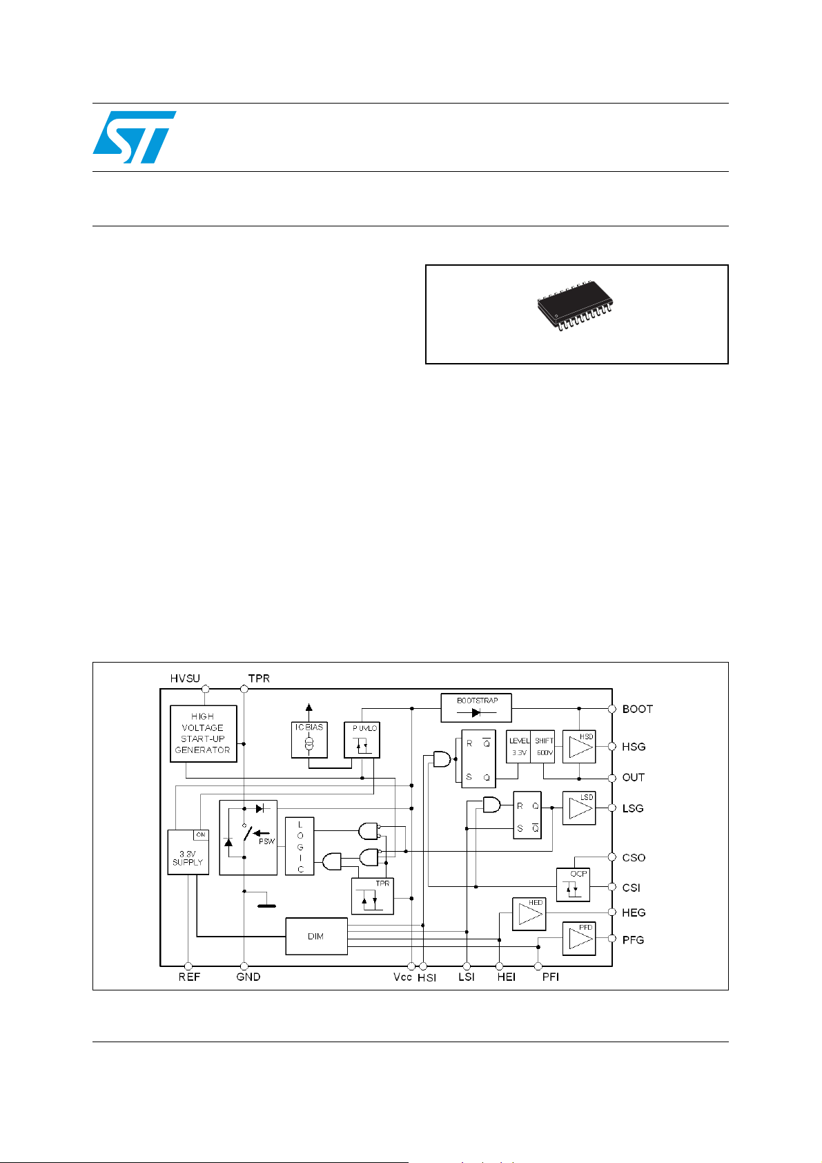
Figure 1. Block diagram
Besides increasing the application efficiency, the
L6382D reduces the bill of materials because
different tasks (regarding drivers and power
management) are performed by a single IC, which
improves the application reliability.
µ
March 2007 Rev 6 1/22
www.st.com
22

Contents L6382D
Contents
1 Device description . . . . . . . . . . . . . . . . . . . . . . . . . . . . . . . . . . . . . . . . . . 3
2 Pin settings . . . . . . . . . . . . . . . . . . . . . . . . . . . . . . . . . . . . . . . . . . . . . . . . 4
2.1 Pin connection . . . . . . . . . . . . . . . . . . . . . . . . . . . . . . . . . . . . . . . . . . . . . . 4
2.2 Pin description . . . . . . . . . . . . . . . . . . . . . . . . . . . . . . . . . . . . . . . . . . . . . . 4
3 Maximum ratings . . . . . . . . . . . . . . . . . . . . . . . . . . . . . . . . . . . . . . . . . . . . 6
3.1 Absolute maximum ratings . . . . . . . . . . . . . . . . . . . . . . . . . . . . . . . . . . . . . 6
3.2 Thermal data . . . . . . . . . . . . . . . . . . . . . . . . . . . . . . . . . . . . . . . . . . . . . . . 6
4 Electrical characteristics . . . . . . . . . . . . . . . . . . . . . . . . . . . . . . . . . . . . . 7
5 Typical electrical performance . . . . . . . . . . . . . . . . . . . . . . . . . . . . . . . . 11
6 Application information . . . . . . . . . . . . . . . . . . . . . . . . . . . . . . . . . . . . . 12
6.1 Power management . . . . . . . . . . . . . . . . . . . . . . . . . . . . . . . . . . . . . . . . . 12
6.1.1 START-UP mode . . . . . . . . . . . . . . . . . . . . . . . . . . . . . . . . . . . . . . . . . . 12
6.1.2 SAVE Mode . . . . . . . . . . . . . . . . . . . . . . . . . . . . . . . . . . . . . . . . . . . . . . 13
6.1.3 OPERATING Mode . . . . . . . . . . . . . . . . . . . . . . . . . . . . . . . . . . . . . . . . 13
6.1.4 Shut down . . . . . . . . . . . . . . . . . . . . . . . . . . . . . . . . . . . . . . . . . . . . . . . 13
7 Block description . . . . . . . . . . . . . . . . . . . . . . . . . . . . . . . . . . . . . . . . . . 16
7.1 Supply section . . . . . . . . . . . . . . . . . . . . . . . . . . . . . . . . . . . . . . . . . . . . . 16
7.2 3.3V reference voltage . . . . . . . . . . . . . . . . . . . . . . . . . . . . . . . . . . . . . . . 16
7.3 Drivers . . . . . . . . . . . . . . . . . . . . . . . . . . . . . . . . . . . . . . . . . . . . . . . . . . . 17
7.4 Internal logic, over current protection (OCP) and interlocking function . . 17
8 Package mechanical data . . . . . . . . . . . . . . . . . . . . . . . . . . . . . . . . . . . . 18
9 Order codes . . . . . . . . . . . . . . . . . . . . . . . . . . . . . . . . . . . . . . . . . . . . . . . 20
10 Revision history . . . . . . . . . . . . . . . . . . . . . . . . . . . . . . . . . . . . . . . . . . . 21
2/22
L6382D Device description
1 Device description
Designed in High-voltage BCD Off-line technology, the L6382D is a PFC and ballast
controller provided with 4 inputs pin and a high voltage start-up generator conceived for
applications managed by a microcontroller providing the maximum flexibility. It allows the
designer to use the same ballast circuit for different lamp wattage/type by simply changing
the µC software.
The digital input pins - able to receive signals up to 400KHz - are connected to level shifters
that provide the control signals to their relevant drivers; in particular the L6382D embeds
one driver for the PFC pre-regulator stage, two drivers for the ballast half-bridge stage (High
Voltage, including also the bootstrap function) and the last one to provide supplementary
features like preheating of filaments supplied through isolated windings in dimmable
applications.
A precise reference voltage (+3.3V ±1%) able to provide up to 30mA is available to supply
the µC: this current is obtained thanks to the on-chip high voltage start-up generator that,
moreover, keeps the consumption before start-up below 150µA.
The chip has been designed with advanced power management logic to minimize power
losses and increase the application reliability.
In the half-bridge section, a patented integrated bootstrap section replaces the external
bootstrap diode.
The L6382D integrates also a function that regulates the IC supply voltage (without the need
of any external charge pump) and optimizes the current consumption.
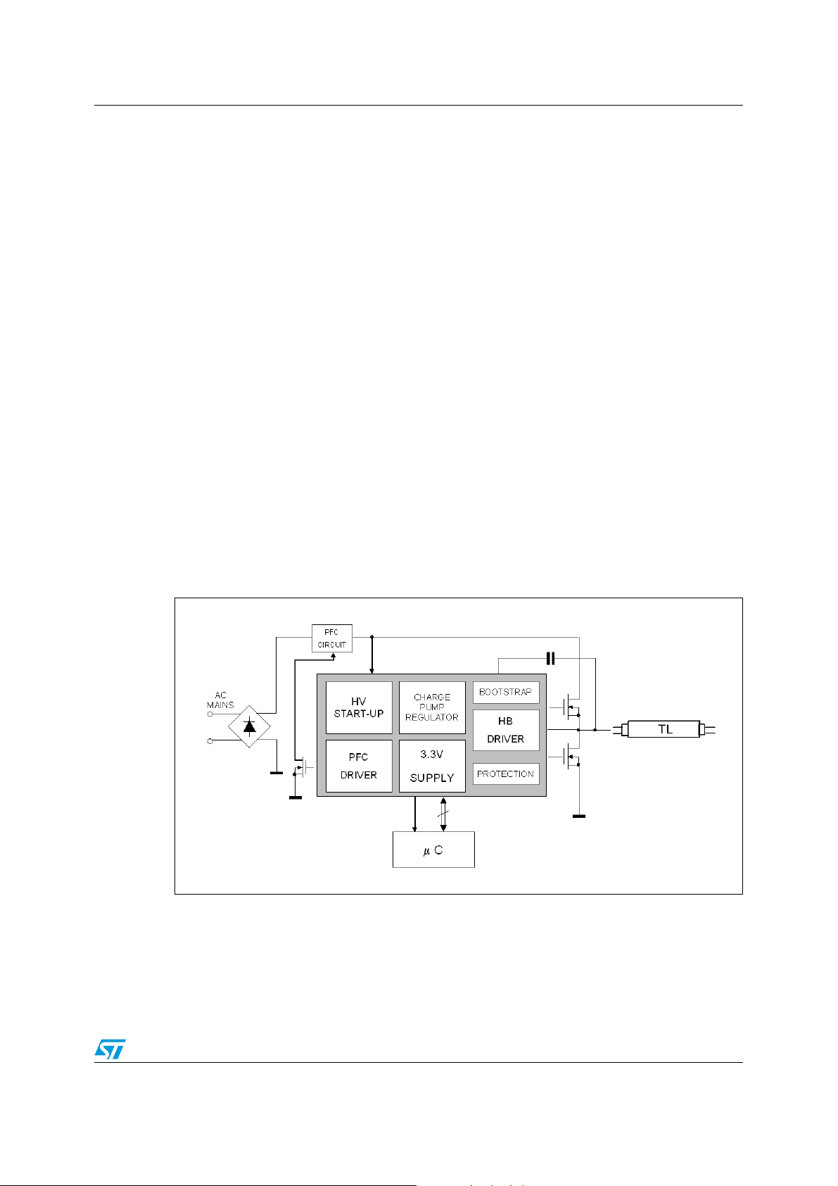
Figure 2. Typical system block diagram
3/22
Pin settings L6382D
2 Pin settings
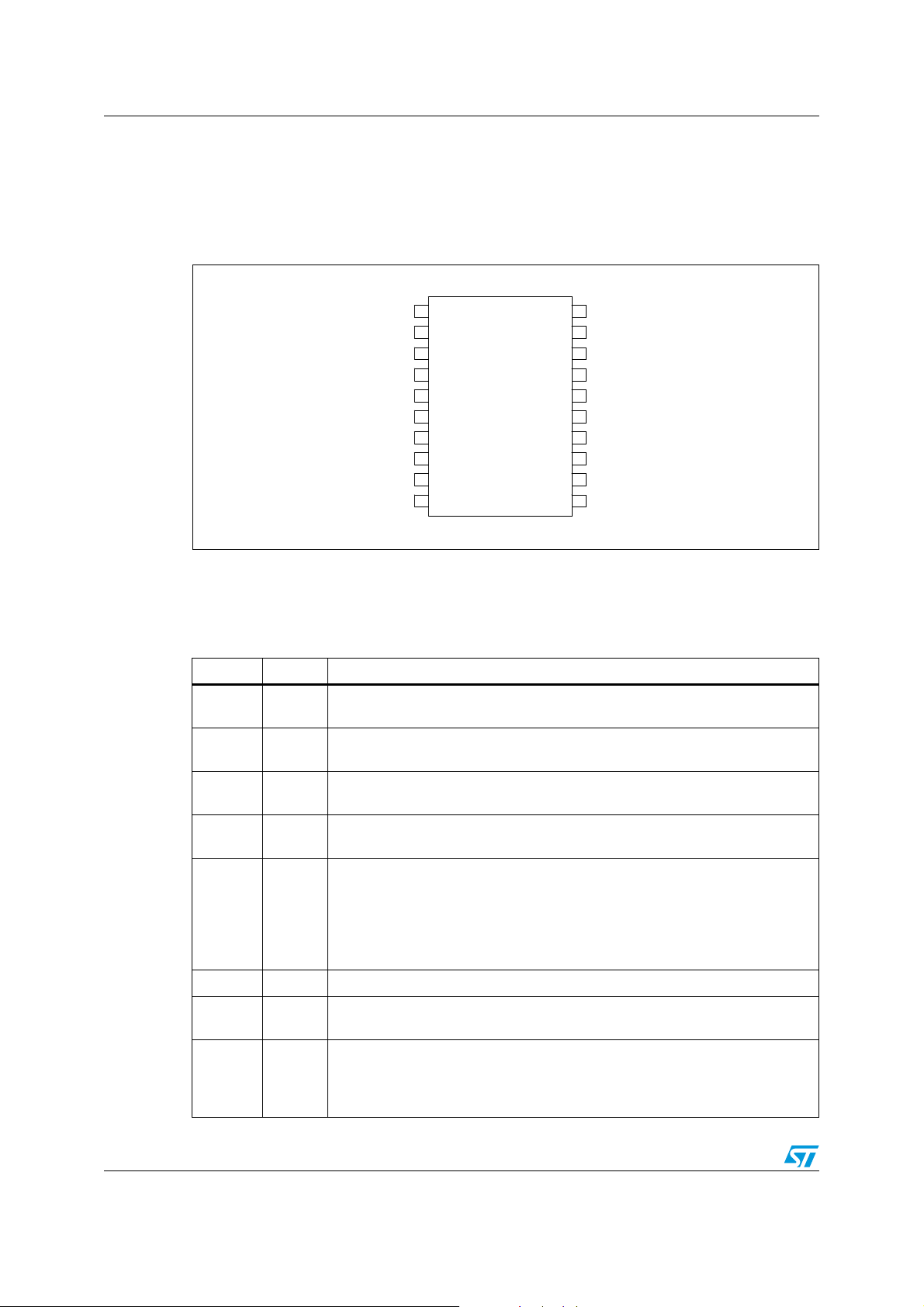
2.1 Pin connection
Figure 3. Pin connection (top view)
2.2 Pin description
Table 1. Pin description
Name Pin N° Description
1PFI
2LSI
3HSI
Digital input signal to control the PFC gate driver. This pin has to be connected
to a TTL compatible signal.
Digital input signal to control the half-bridge low side driver. This pin has to be
connected to a TTL compatible signal.
Digital input signal to control the half-bridge high side driver. This pin has to be
connected to a TTL compatible signal.
PFI
PFI
LSI
LSI
HSI
HSI
HEI
HEI
PFG
PFG
N.C.
N.C.
TPR
TPR
GND
GND
LSG
LSG
VCC
VCC
1
1
2
2
3
3
4
4
5
5
6
6
7
7
8
8
9
9
10
10
20
20
19
19
18
18
17
17
16
16
15
15
14
14
13
13
12
12
11
11
VREF
VREF
CSI
CSI
CSO
CSO
HEG
HEG
N.C.
N.C.
HVSU
HVSU
N.C.
N.C.
OUT
OUT
HSG
HSG
BOOT
BOOT
4HEI
5PFG
6 N.C. Not connected
7TPR
8GND
4/22
Digital input signal to control the HEG output. This pin has to be connected to a
TTL compatible signal.
PFC Driver Output. This pin is intended to be connected to the PFC power
MOSFET gate. A resistor connected between this pin and the power MOS gate
can be used to reduce the peak current. An internal 10KΩ resistor toward
ground avoids spurious and undesired MOSFET turn-on. The totem pole
output stage is able to drive the power MOS with a peak current of 120mA
source and 250mA sink.
Input for two point regulator; by coupling the pin with a capacitor to a switching
circuit, it is possible to implement a charge circuit for the Vcc.
Chip ground. Current return for both the low-side gate-drive currents and the
bias current of the IC. All of the ground connections of the bias components
should be tied to a trace going to this pin and kept separate from any pulsed
current return.

L6382D Pin settings
Table 1. Pin description
Name Pin N° Description
Low Side Driver Output. This pin must be connected to the gate of the halfbridge low side power MOSFET. A resistor connected between this pin and the
power MOS gate can be used to reduce the peak current.
9LSG
10 Vcc Supply Voltage for the signal part of the IC and for the drivers.
11 BOOT
12 HSG
13 OUT
14 N.C. Not connected
An internal 20KΩ resistor toward ground avoids spurious and undesired
MOSFET turn-on.
The totem pole output stage is able to drive power with a peak current of
120mA source and 120mA sink.
High-side gate-drive floating supply Voltage. The bootstrap capacitor
connected between this pin and pin 13 (OUT) is fed by an internal
synchronous bootstrap diode driven in phase with the low-side gate-drive. This
patented structure normally replaces the external diode.
High Side Driver Output. This pin must be connected to the gate of the half
bridge high side power MOSFET . A resistor connected between this pin and
the power MOS gate can be used to reduce the peak current.
An internal 20KΩ resistor toward OUT pin avoids spurious and undesired
MOSFET turn-on
The totem pole output stage is able to drive the power MOS with a peak
current of 120mA source and 120mA sink.
High-side gate-drive floating ground. Current return for the high-side gate-drive
current. Layout carefully the connection of this pin to avoid too large spikes
below ground.
15 HVSU
16 N.C.
17 HEG
18 CSO
19 CSI
20 VREF
High-voltage start-up. The current flowing into this pin charges the capacitor
connected between pin Vcc and GND to start up the IC. Whilst the chip is in
mode, the generator is cycled on-off between turn-on and save mode
save
voltages. When the chip works in operating
and it is re-enabled when the Vcc voltage falls below the UVLO threshold.
According to the required V
rectified mains voltage either directly or through a resistor.
High-voltage spacer. The pin is not connected internally to isolate the highvoltage pin and comply with safety regulations (creepage distance) on the
PCB.
Output for the HEI block; this driver can be used to drive the MOS employed in
isolated filaments preheating. An internal 20KΩ resistor toward ground avoids
spurious and undesired MOSFET turn-on.
Output of current sense comparator, compatible with TTL logic signal; during
operating
triggered (CSI> 0.5V typ.) the pin latches high.
Input of current sense comparator, it is enabled only during operating mode;
when the pin voltage exceeds the internal threshold, the CSO pin is forced
high and the half bridge drivers are disabled. It exits from this condition by
either cycling the Vcc below the UVLO or with LGI=HGI=low simultaneously.
Voltage reference. During normal mode an internal generator provides an
accurate voltage reference that can be used to supply up to 30mA (during
operating mode) to an external circuit. A small film capacitor (0.22µF min.),
connected between this pin and GND is recommended to ensure the stability
of the generator and to prevent noise from affecting the reference.
mode, the pin is forced low whereas whenever the OC comparator is
pin current, this pin can be connected to the
REF
mode the generator is shut down
5/22

Maximum ratings L6382D
3 Maximum ratings
3.1 Absolute maximum ratings
Table 2. Absolute maximum ratings
Symbol Pin Parameter Value Unit
V
CC
V
HVSU
V
BOOT
V
OUT
I
TPR(RMS)
I
TPR(PK)
V
TPR
10 IC supply voltage (ICC = 20mA) Self-limited
15 High voltage start-up generator voltage range -0.3 to 600 V
11 Floating supply voltage
-1 to V
HVSU+VCC
13 Floating ground voltage -1 to 600 V
7 Maximum TPR RMS current ±200 mA
7 Maximum TPR peak current ±600 mA
7
Maximum TPR voltage
(1)
14 V
19 CSI input voltage -0.3 to 7 V
1, 2,
Logic input voltage -0.3 to 7 V
3, 4
9, 12,
Operating frequency 15 to 400 KHz
17
V
5 Operating frequency 15 to 600 KHz
Tstg Storage temperature -40 to +150 °C
T
J
1. Excluding operating mode
3.2 Thermal data
Table 3. Thermal data
Symbol Parameter Value Unit
R
thJA
Maximum thermal resistance junction-ambient 120 °C/W
Ambient temperature operating range -40 to +125 °C
6/22
L6382D Electrical characteristics
4 Electrical characteristics
Table 4. Electrical characteristcs (TJ = 25°C, VCC = 13V, C
unless otherwise specified)
DRIVER
= 1nF
Symbol Pin Parameter Test condition Min Typ Max Unit
Supply voltage
V
CCON
V
CCOFF
V
CCSM
VSMhys 10
V
REF(OFF)
10 Turn-on voltage 13 14 15 V
10 Turn-off voltage 7.5 8.25 9.2 V
10 Save mode voltage 12.75 13.8 14.85 V
Save mode
hysteresys
0.12 0.16 0.2 V
10 Reference turn-off 5.7 6 6.4 V
IvccON 10 Start-up current 150 µA
IvccSM 10
Ivcc 10
Save Mode current
consumption
Quiescent current
in operating mode
(1) 150 230 µA
LGI = HGI = high;
no load on VREF.
190 µA
2mA
Vz 10 Internal Zener 16.5 17 18 V
High voltage start-up
> 50V
IMSS 15 Maximum current
ILSS 15
Leakage current off
state
V
HVSU
V
HVSU
= 600V
20 mA
40 µA
Two point regulator (TPR) protection
T
PR
st
PR
T
(ON)
T
PR
(OFF)
Vcc Protection
10
level
10 Vcc Turn-on level
10 Vcc Turn-off level
Output voltage on
7
state
Forward voltage
7
drop Diode
Leakage current off
7
state
Operating mode 14.0 14.5 15.0 V
Operating mode; after
the first falling edge on
12.5 13 13.5 V
LSG
Operating mode; after
the first falling edge on
12.45 12.95 13.48 V
LSG
= 200mA
I
TPR
@ 600mA forward
current.
V
= 13V
TPR
2V
2.3 V
5µA
7/22
 Loading...