

L6376
0.5A HIGH-SIDE DRIVER
QUAD INTELLIGENTPOWERSWITCH
0.5 AFOURINDEPENDENTOUTPUTS
9.5 TO 35 V SUPPLYVOLTAGERANGE
INTERNALCURRENT LIMIT
NON-DISSIPATIVE OVER-CURRENT PRO-
TECTION
THERMALSHUTDOWN
UNDER VOLTAGE LOCKOUT WITH HYS-
TERESYS
DIAGNOSTIC OUTPUT FOR UNDER VOLT-
AGE, OVER TEMPERATURE AND OVER
CURRENT
EXTERNAL ASYNCHRONOUS RESET INPUT
PRESETTABLE DELAY FOR OVERCURRENT DIAGNOSTIC
OPENGROUND PROTECTION
IMMUNITY AGAINST BURST TRANSIENT
(IEC801-4)
ESDPROTECTION (HUMAN BODY MODEL ±
2KV)
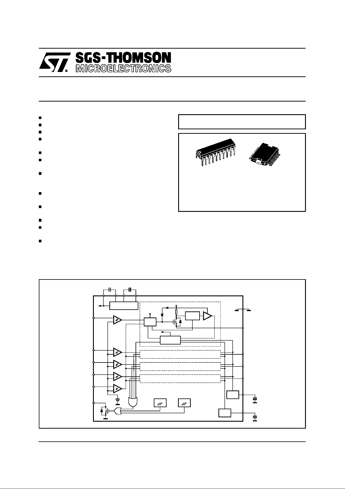
BLOCK DIAGRAM
220nF 22nF
V
V
S
CP
VCV
P
MULTIPOWERBCD TECHNOLOGY
POWERDIP
16+2+2
ORDERING NUMBERS:L6376 (DIP
PowerSO20
L6376PD (PSO)
DESCRIPTION
This device is a monolithic quad Intelligent Power
Switch in MultipowerBCD Technology, for driving
inductive,capacitive or resistive loads. Diagnostic
for CPU feedbackand extensive use of electrical
protections make this device inherently indistructible and suitable for general purpose industrial applications.
November 1996
DIAG
V
S
I
1
I
2
I
3
I
4
R
CHARGE PUMP
+
-
+
-
+
-
+
-
+
-
1.25V
V
CP
DRIVER
V
S
R
S
UV
SHORT
CIRCUIT
CONTROL
OVT UV
CURRENT
LIMIT
OVC
OSC
GND
O
1
O
2
O
3
O
4
OFF DELAY
OFF
OSC
C
DOFF
D94IN076C
ON DELAY
C
DON
ON
1/12

L6376
ABSOLUTE MAXIMUM RATINGS (Pinnumering referredto PowerSO20package)
Symbol Pin Parameter Value Unit
V
s
Supply Voltage (t
6
Supply Voltage (DC) 40 V
V
s-Vout
id
V
I
id
I
i
16,17
12,13 ,
Difference between supply voltage and output voltage internally limited
Externally Forced Voltage -0.3 to 7 V
Externally Forced Current
Channel Input Current (forced) ±2mA
14,15 ,
i Channel Input Voltage -0.3 to 40 V
V
18
< 10ms) 50 V
w
1mA
±
I
out
out Output Voltage internally limited
V
E
il
P
tot
diag
V
I
diag
T
op
T
j
stg Storage temperature -55 to 150 °C
T
2, 3,
8, 9
Output Current (see also I
Energy Inductive Load (Tj=125°C); Each Channel 200 mJ
Power Dissipation internally limited
External voltage -0.3 to V
19
Externally forced current -10 to 10 mA
Ambient temperature, operating range -25 to 85 °C
Junction temperature, operating range (see
Overtemperature Protection)
) internally limited
sc
+0.7 V
s
-25 to 125
PIN CONNECTIONS (Topview)
V
V
CP
O
O
GND
GND
1
S
2
3
2
4
1
5
6
I
7
1
I
8
2
I
9 OFF DELAY
3
I
10 ON DELAY11
4
D93IN030B
20
19
18
17
16
15
14
13
12
V
C
V
P
O
3
O
4
GND
GND
DIAG
R
GND
O4
O3
VP
VC
V
S
VCP
O2
O1
GND 10
1
2
3
4
5
6
7
8
9
D95IN217
20
19
18
17
16
15
14
13
12
11
GND
DIAG
R
OFF DELAY
ON DELAY
I4
I3
I2
I1
GND
C
°
2/12
POWERDIP
PowerSO20

PIN DESCRIPTION(Pin numering referred to PowerSO20package).
No Pins Function
Positive supply voltage.
6V
7V
2, 3,
8, 9
1, 10,
11, 20
12,13,
14, 15
S
CP
O
1,O2,O3,O4
GND
I
1,I2,I3,I4
16 ON DELAY
17 OFF DELAY
18 R
19 DIAG
5V
4V
C
P
An internal circuit, monitoring the supply voltage, maintainsthe IC in off-state until V
reaches 9V or when VSfalls under 8.5V.
The diagnostic is availlable since V
S
= 5V.
Switch driver supply.
To minimize the output drop voltage, a supply of about 10V higher than V
order to use the built-in charge pump, connect a filtercapacitor from pin1 to pin.
The suggested value assures a fast transition and a low supply ripple even in worse
condition. Using the four channels contemporarily, values less than 68nF haveto be
avoided.
High side outputs.
Four independently controlled outputs with built-in current limitation.
Ground and power dissipating pins.
These pins are connected to the bulk ground of the IC, so are useful for heat dissipation.
Control inputs.
Four independent control signals. The outputis held off until the voltage at the
corresponding input pinreaches 1.35V and is turned off when the voltage at the pin goes
below 1.15V.
Programmable ON duration in short circuit.
If an output is short circuited to ground or carryng a current exceeding the limit, the output
is turned-off and the diagnostic activation are delayed. This procedure allows the driving
of hard surge current loads.
The delay is programmed connecting a capacitor (50pF to 15nF) versus ground with the
internal timeconstant of 1.28µs/pF. The function can be disabled short circuiting this pin
to ground.
Programmable OFF duration in short circuit.
After the short circuit or overcurrent detection, the switchis held off before the next
attempt to switch onagain.
The delay is programmed connecting a capacitor (50pF to 15nF) versus ground with the
internal timeconstant of 1.28µs/pF.
Short circuiting this pin to ground the OFF delay is 64 times the ON delay.
Asyncronous reset input.
This active low input (with hysteresis), switch off all the outputs independently from the
input signal. By default itis biased low.
Diagnostic output.
This open drain output reports the IC working condition. The bad condition (as
undervoltage, overcurrent, overtemperature) turns the output low.
Pump oscillator voltage.
At this pin is available the built-in circuitry to supply the switch driver at about 10V higher
. To use thisfeature, connect a capacitor across pin 4 and pin 5.
than V
S
The suggested value assures a fast transition and a minimum output drop voltage even in
worse condition. Using the four channels contemporarily, values less than 6.8nF have to
be avoided.
Bootstrapped voltage.
At this pin is available the 11V oscillation for the charge pump, at a typical frequency of
200kHz.
is required. In
S
L6376
S
3/12
L6376
ELECTRICALCHARACTERISTICS(Vs= 24V;Tj= -25 to 125°C; unlessotherwise specified.)
DC OPERATION(Pin numeringreferred to PowerSO20package).
Symbol Pin Parameter Test Condition Min. Typ. Max. Unit
s
V
V
sth
V
shys
qsc Quiescent Current Outputs ON, No load 3 5 mA
I
V
il
V
ih
I
bias
ihys Input Comparators Hysteresis 100 200 400 mV
V
Θ
lim
Θ
H
I
sc
I
olk
V
cl
V
ol
dlkg
I
V
diag
I
dch
12,13,
14,15,
16,17
Supply Voltage 9.5 24 35 V
UV UpperThreshold 8.5 9 9.5 V
6
UV Hysteresis 200 500 800 mV
Input Low Level 0 0.8 V
Input High Level 2 40 V
=0V -5 -1 0
V
Input Bias Current
18
i
= 40V 0 5 20 µA
V
i
OVT Upper Threshold 150
Threshold Hysteresis 20 30 °C
Short Circuit Current V
Output Voltage Drop
2, 3,
8, 9
Output Leakage Current Vo=0V; Vi<0.8V 100
Internal Voltage Clamp
each Output)
(V
s-Vo
Low State Output Voltage Vi=Vil;RL=
=9.5 to 35V; Rl=2Ω 0.65 0.9 1.2 A
s
=500mA; Tj=25°C 320 500 mV
I
out
out =500mA; T
I
I
=100mA
o
single pulsed T
=125°C 460 640 mV
j
p
∞
=300µs
47 52 57 V
0.8 1.5 V
Diagnostic Output Leakage Diagnostic Off 25 µA
19
Diagnostic Output Voltage
Drop
Delay Capacitors Charge
Current
= 5mA 1.5 V
I
diag
40
A
µ
C
°
A
µ
A
µ
4/12

AC OPERATION(Pin numeringreferred to PowerSO20package).
Symbol Pin Parameter Test Condition Min. Typ. Max. Unit
tr-t
t
2,3,8,9 Rise orFall Time
f
12vs9
d
13vs8
14 vs3
Delay Time 1 µs
Vs= 24V;Rl=47Ω
to ground
R
l
3.8
15vs2
dV/dt
t
ON
t
OFF
f
max
2, 3,
8, 9
16
17
Slew Rate (Rise and Fall
Edge)
On Time during Short
Circuit Condition
Off Time during Short
Circuit Condition
Maximum Operating
Frequency
= 24V;Rl=47ΩRISE
V
s
to ground FALL34
R
l
50 pF < C
< 15nF 1.28
DON
5
7.6
pin 13grounded 64 t
50pF <C
< 15nF 1.28
DOFF
25 kHz
7
10
SOURCEDRAIN NDMOSDIODE
Symbol Parameter Test Condition Min. Typ. Max. Unit
V
fsd
I
fp
t
rr
t
fr
Forward On Voltage I
Forward Peak Current tp= 10ms; dutycycle = 20% 1.5 A
Reverse Recovery Time I
Forward Recovery Time 50 ns
= 500mA 1 1.5 V
fsd
= 500mA; dI
fsd
/dt = 25A/µs 200 ns
fsd
L6376
s
µ
V/µs
s/pF
µ
ON
s/pF
µ
UNDERVOLTAGE COMPARATOR HYSTERESIS
V
SWITCHINGWAVEFORMS
V
in
50% 50%
t
d
V
out
90% 90%
50% 50%
10% 10%
t
r
shys
D94IN126A
V
sth
V
s
D94IN127A
t
t
t
d
t
f
5/12

L6376
THERMAL DATA
Symbol Parameter DIP16+2+2 PowerSO20 Unit
R
thj-pin
thj-amb1
R
R
thj-amb2
R
th j-case
Thermal Resistance, Junctionto Pin 12 –
Thermal Resistance, Junctionto Ambient
(see Thermal Characteristics)
Thermal Resistance, Junctionto Ambient (see Thermal
Characteristics)
Thermal Residance Junction-case – 1.5
40 – °C/W
50 – °C/W
C/W
°
C/W
°
THERMAL CHARACTERISTICS
R
th j-pins
DIP16+2+2. The thermal resistance is referred to the thermal path from the dissipating region on the top surface of the silicon
chip, to the points along the four central pins
of the package, at a distance of 1.5 mm
away from the stand-offs.
R
th j-amb1
If a dissipating surface, thick at least 35 µm,
and with a surface similar or bigger than the
one shown, is created making use of the
printed circuit.
Such heatsinking surface is considered on
the bottom side of an horizontal PCB (worst
case).
R
th j-amb2
If the power dissipatingpins (the four central
ones), as well as the others, have a mini-
Figure 1: PrintedHeatsink
mum thermal connection with the external
world (very thin strips only) so that the dissipation takes place through still air and
throughthe PCB itself.
It is the same situation of point above, without any heatsinking surface created on purpose on theboard.
Addition al data on the PowerDip and the
PowerSO20 pa ckage can b e foun d in:
ApplicationNote AN467:
ThermalCharacteristics of the PowerDip
20,24Packages Solderedon 1,2,3 oz.
CopperPCB
ApplicationNote AN668:
A New High Power IC Surface Mount Package: PowerSO20 Power IC Packaging from
Insertionto SurfaceMounting.
6/12

L6376
OVERTEMPERATURE PROTECTION(OVT)
If the chip temperature exceeds
Θ
(measuredin
lim
a central position in the chip) the chip deactivates
itself.
The followingactions are taken:
•
all theoutput stagesare switchedoff;
•
the signal DIAGis activated (activelow).
Normal operation is resumedas soon as (typically
after some seconds) the chip temperature monitored goes backbelow Θ
lim-ΘH
.
The different thresholds with hysteretic behavior
assure thatno intermittent conditions can be generated.
UNDERVOLTAGE PROTECTION(UV)
The supply voltage is expected to range from
9.5V to 35V, even if its reference value is considered tobe 24V.
In this rangethe deviceoperates correctly.
Below 9.5V the overall system has to be considered notreliable.
Consequently the supply voltage is monitored
continuously and a signal, called UV, is internally
generatedand used.
The signal is “on” as long as the supply voltage
does not reachthe upper internal thresholdof the
comparator V
V
s
above V
sth
.
. The UV signal disappears
sth
Once the UV signal has been removed, the supply voltage must decrease below the lower
threshold (i.e. V
sth-Vshys
) before it is turned on
again.
The hysteresis V
is provided to prevent inter-
shys
mittent operation of the device at low supply voltages that may have a superimposed ripple
aroundthe averagevalue.
The UV signal switches off the outputs, but has
no effecton the creationof thereferencevoltages
for the internal comparators, nor on the continuous operation of the charge-pumpcircuits.
DIAGNOSTIC LOGIC
The situations that are monitored and signalled
with the DIAGoutput pin are:
• currentlimit (OVC)in action; there are 4 individual current limiting circuits, one per each
output;theylimit the currentthat can be sunk
from each output, to a typical value of
800mA,equal for all of them;
• undervoltage (UV);
• overtemperature protection (OVT).
The diagnostic signal is transmitted via an open
drain output (for ease of wired-or connection of
several such signals) and a low level represents
the presence of at leastoneof themonitored conditions,mentionedabove.
SHORT CIRCUITOPERATION
In order to allow normal operation of the other inputs when one channel is in short cirtuit, an innovativenon dissipativeover current protection(patent pending)is implementedin the device.
Figure 2: ShortCircuit OperationWaveforms
OUTPUT
CURRENT
I
sc
I
out
t<t
ON
DIAG
(active low)
t
ON
t
OFF
Short CircuitShort Circuit
t
ON
t
OFF
D94IN105
Time
Time
7/12

L6376
In this way, the temperature of the device is kept
enough low to preventtheintervention of the thermal protection (in most of the cases) and so to
avoid theshut down of the whole device.
If a short circuit condition is present on one output, the current limiting circuit puts that channelin
linear mode — sourcing the I
800 mA) — for a time period (t
external capacitor (C
DON
current (typically
SC
) defined by an
ON
connected to the ON
DELAY pin).
After that period, if the short circuit condition is
still present the output is turned off for another
time period (t
capacitor (C
) defined by a second external
OFF
connected to the OFF DELAY
DOFF
pin).
When also this period is expired:
•
if the short circuit condition is still present the
output stays on for the t
period and the se-
ON
quence startsagain;
• if the short circuit condition is not present
anymore the normal operation of the output
is resumed.
The t
ON
and t
periods are completely inde-
OFF
pendent and can be set from 64 µs to 15 ms, us-
ing external capacitors ranging from 50 pF to
15 nF (1.28 µs/pF).
If the OFF DELAY pin is tied to ground (i.e. the
C
capacitor is not used) the t
DOFF
is 64 times the t
ON
period.
time period
OFF
The diagnostic output (DIAG) is active when the
output is switched off, while it is not active when
the output is on (i.e. during the t
period)even if
ON
in that period a shortcircuit condition is present.
Typical waveforms for short circuit operation are
shown in figure 2.
If both the ON DELAY and the OFF DELAY pins
are grounded the non dissipative over current
protection is inhibited and the outputsin short circuit remain on until the thermal shutdown switch
off the whole device. In this case the short circuit
condition is not signalled by the DIAG pin (that
continues to signal the under voltage and over
temperature conditions).
PROGRAMMABLE DIAGNOSTIC DELAY
The current limiting circuits can be requested to
perform even in absence of a real fault condition,
for a short period, if the load is of capacitive nature or if it is a filament lamp (that exhibits a very
low resistance during the initial heating phase).
To avoid the forwarding of misleading— i.e. short
diagnostic pulses in coincidence with the intervention of the current limiting circuits when operating on capacitive loads — the activation of the
diagnostic can be delayed with respect to the interventionof one of the current limiting circuits.
This delay can be defined by an external capacitor (C
) connectedbetween theONDELAY pin
DON
and ground.
RESETINPUT
An external reset input R (pin 18) is provided to
simultaneously switch off all the outputs: this signal (active low) is in effectan asynchronous reset
that keeps the outputs low independentlyfrom the
input signals.
For example, this reset input can be used by the
CPU to keep the outputs low after a fault condition (signaled by theDIAG pin).
DEMAGNETIZATION OF INDUCTIVE LOADS
The devicehas four internal clamping diodes able
to demagnetizeinductiveloads.
The limitation is the peak power dissipation of the
packages, so — if the loads are big or if there is
the possibility to demagnetize more loads contemporarly — it is necessary to use external demagnetizationcircuits.
In figures 4 and 5 are shown two topologies for
the demagnetization versus ground and versus
.
V
S
The breakdown voltage of the external device
(V
) must be chosen considering the minimum in-
Z
ternal clamping voltage (V
supplyvoltage(V
).
S
) and the maximum
cl
Figure3: InputComparator Hysteresis
V
out
V
s
8/12
100mV
1.25V
100mV
D94IN131
V
i

Figure 4: ExternalDemagnetizationCircuit (versus ground)
V
S
V
CP
DRIVER
UV
SHORT CIRCUIT
CONTROL
R
S
CURRENT
LIMIT
OVC
L6376
O
1
O
2
O
3
O
4
D94IN109
VZ<V
cl (min)-VS (max)
Figure 5: ExternalDemagnetizationCircuit (versus VS)
V
S
V
CP
DRIVER
UV
SHORT CIRCUIT
CONTROL
R
S
CURRENT
LIMIT
OVC
V
Z
V
S
V
Z
O
1
O
2
O
3
O
4
D94IN110A
V
S (max)<VZ<Vcl (min)
9/12

L6376
POWERDIP20 PACKAGEMECHANICAL DATA
DIM.
MIN. TYP. MAX. MIN. TYP. MAX.
a1 0.51 0.020
B 0.85 1.40 0.033 0.055
b 0.50 0.020
b1 0.38 0.50 0.015 0.020
D 24.80 0.976
E 8.80 0.346
e 2.54 0.100
e3 22.86 0.900
F 7.10 0.280
I 5.10 0.201
mm inch
10/12

PowerSO20PACKAGE MECHANICAL DATA
L6376
DIM.
mm inch
MIN. TYP. MAX. MIN. TYP. MAX.
A 3.60 0.1417
a1 0.10 0.30 0.0039 0.0118
a2 3.30 0.1299
a3 0 0.10 0 0.0039
b 0.40 0.53 0.0157 0.0209
c 0.23 0.32 0.009 0.0126
D (1) 15.80 16.00 0.6220 0.6299
E 13.90 14.50 0.5472 0.570
e 1.27 0.050
e3 11.43 0.450
E1 (1) 10.90 11.10 0.4291 0.437
E2 2.90 0.1141
G 0 0.10 0 0.0039
h 1.10
L 0.80 1.10 0.0314 0.0433
N10°(max.)
S8°(max.)
T 10.0 0.3937
(1) ”D and E1” do not includemold flash or protrusions
- Moldflashor protrusions shall not exceed 0.15mm (0.006”)
E2
hx45°
NN
a2
A
b
DETAIL A
110
e3
D
T
e
1120
E1
R
DETAILB
PSO20MEC
lead
a3
Gage Plane
E
DETAILB
0.35
S
L
c
a1
DETAIL A
slug
-C-
SEATINGPLANE
GC
(COPLANARITY)
11/12

L6376
Information furnished is believed to be accurate and reliable. However, SGS-THOMSON Microelectronicsassumes no responsibility for the
consequences of use of such information nor for any infringement of patents or other rights of third parties which may result from its use. No
license is grantedby implication or otherwise under any patentor patent rightsof SGS-THOMSON Microelectronics. Specification mentioned
in this publication are subject tochange without notice. This publication supersedes and replaces all information previously supplied. SGSTHOMSON Microelectronics products are not authorized for use as critical components in life support devices or systems without express
written approvalof SGS-THOMSON Microelectronics.
1996 SGS-THOMSON Microelectronics – Printedin Italy – AllRights Reserved
SGS-THOMSON Microelectronics GROUPOF COMPANIES
Australia - Brazil - Canada- China - France - Germany - Hong Kong - Italy - Japan - Korea - Malaysia - Malta- Morocco - The Netherlands-
Singapore - Spain - Sweden - Switzerland - Taiwan - Thailand - United Kingdom - U.S.A.
12/12
 Loading...