

0.5 A high-side driver quad intelligent power switch
Features
■ Multipower BCD technology
■ 0.5 A four independent outputs
■ 9.5 to 35 V supply voltage range
■ Internal current limit
■ Non-dissipative over-current protection
■ Thermal shutdown
■ Under voltage lockout with hysteresys
■ Diagnostic output for under voltage, over
temperature and over current
■ External asynchronous reset input
■ Presettable delay for overcurrent
■ Diagnostic
■ Open ground protection
■ Immunity against burst transient
(IEC 61000-4-4)
■ ESD protection (human body model ± 2 kV)
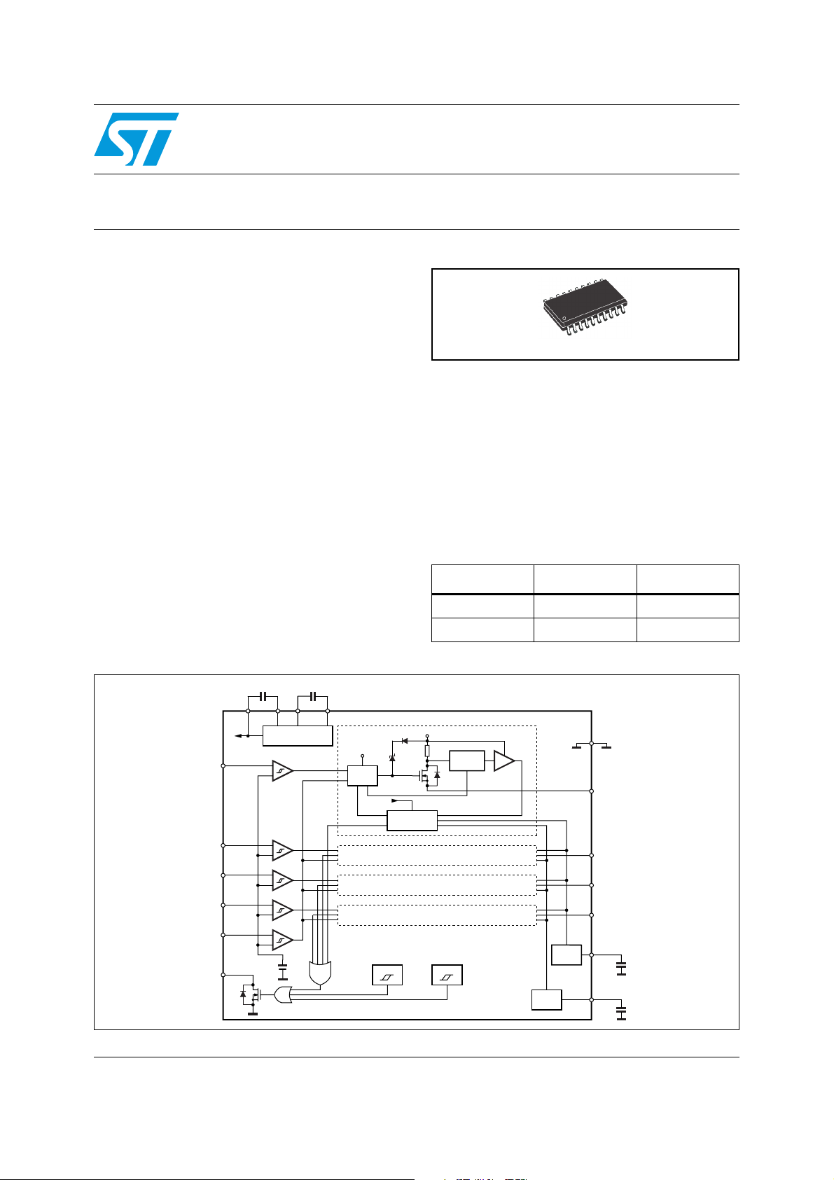
Figure 1. Block diagram
220nF 22nF
V
V
CP
S
VCV
P
L6376
PowerSO-20
Description
This device is a monolithic quad intelligent power
switch in multipower BCD technology, for driving
inductive, capacitive or resistive loads. Diagnostic
for CPU feedback and extensive use of electrical
protections make this device inherently
indistructible and suitable for general purpose
industrial applications.
Table 1. Device summary
Order codes Package Packaging
L6376D PowerSO-20 Tube
L6376D013TR PowerSO-20 Tape and reel
V
S
R
S
UV
SHORT CIRCUIT
CONTROL
OVT UV
CURRENT
LIMIT
OVC
OSC
GND
O
1
O
2
O
3
O
4
OFF DELAY
OFF
OSC
C
DOFF
D94IN076C
ON DELAY
C
DON
ON
DIAG
V
S
I
1
I
2
I
3
I
4
R
CHARGE PUMP
+
-
+
-
+
-
+
-
+
-
1.25V
V
CP
DRIVER
March 2008 Rev 6 1/18
www.st.com
18

Contents L6376
Contents
1 Maximum rating . . . . . . . . . . . . . . . . . . . . . . . . . . . . . . . . . . . . . . . . . . . . . 3
2 Pin connections . . . . . . . . . . . . . . . . . . . . . . . . . . . . . . . . . . . . . . . . . . . . . 4
3 Thermal characteristics . . . . . . . . . . . . . . . . . . . . . . . . . . . . . . . . . . . . . . 6
4 Electrical characteristics . . . . . . . . . . . . . . . . . . . . . . . . . . . . . . . . . . . . . 7
5 Overtemperature protection (OVT) . . . . . . . . . . . . . . . . . . . . . . . . . . . . 10
6 Undervoltage protection (UV) . . . . . . . . . . . . . . . . . . . . . . . . . . . . . . . . 10
7 Diagnostic logic . . . . . . . . . . . . . . . . . . . . . . . . . . . . . . . . . . . . . . . . . . . . 10
8 Short circuit operation . . . . . . . . . . . . . . . . . . . . . . . . . . . . . . . . . . . . . . 11
9 Programmable diagnostic delay . . . . . . . . . . . . . . . . . . . . . . . . . . . . . . 12
10 Reset input . . . . . . . . . . . . . . . . . . . . . . . . . . . . . . . . . . . . . . . . . . . . . . . . 12
11 Demagnetization of inductive loads . . . . . . . . . . . . . . . . . . . . . . . . . . . 13
12 Package mechanical data . . . . . . . . . . . . . . . . . . . . . . . . . . . . . . . . . . . . 15
13 Revision history . . . . . . . . . . . . . . . . . . . . . . . . . . . . . . . . . . . . . . . . . . . 17
2/18
L6376 Maximum rating
1 Maximum rating
Table 2. Absolute maximum ratings
Symbol Pin Parameter Value Unit
V
s
- V
V
s
out
V
id
I
id
I
i
6
16, 17
12, 13,
Supply voltage (DC) 40 V
Difference between supply voltage and output
voltage
internally limited
Externally forced voltage -0.3 to 7 V
Externally forced current ±1 mA
Channel input current (forced) ±2 mA
14, 15,
Supply voltage (tw ≤ 10 ms) 50 V
Channel input voltage -0.3 to 40 V
18
Output current (see also I
9
Output voltage internally limited
Energy inductive load (TJ =125 °C);
each channel
) internally limited
sc
200 mJ
Power dissipation internally limited
External voltage -0.3 to Vs+0.7 V
19
Externally forced current -10 to 10 mA
Ambient temperature, operating range -25 to 85 °C
Junction temperature, operating range (see
overtemperature protection)
-25 to 125 °C
V
I
V
E
P
I
diag
T
T
V
out
out
il
tot
diag
op
J
i
2, 3, 8,
T
stg
Storage temperature -55 to 150 °C
3/18
Pin connections L6376
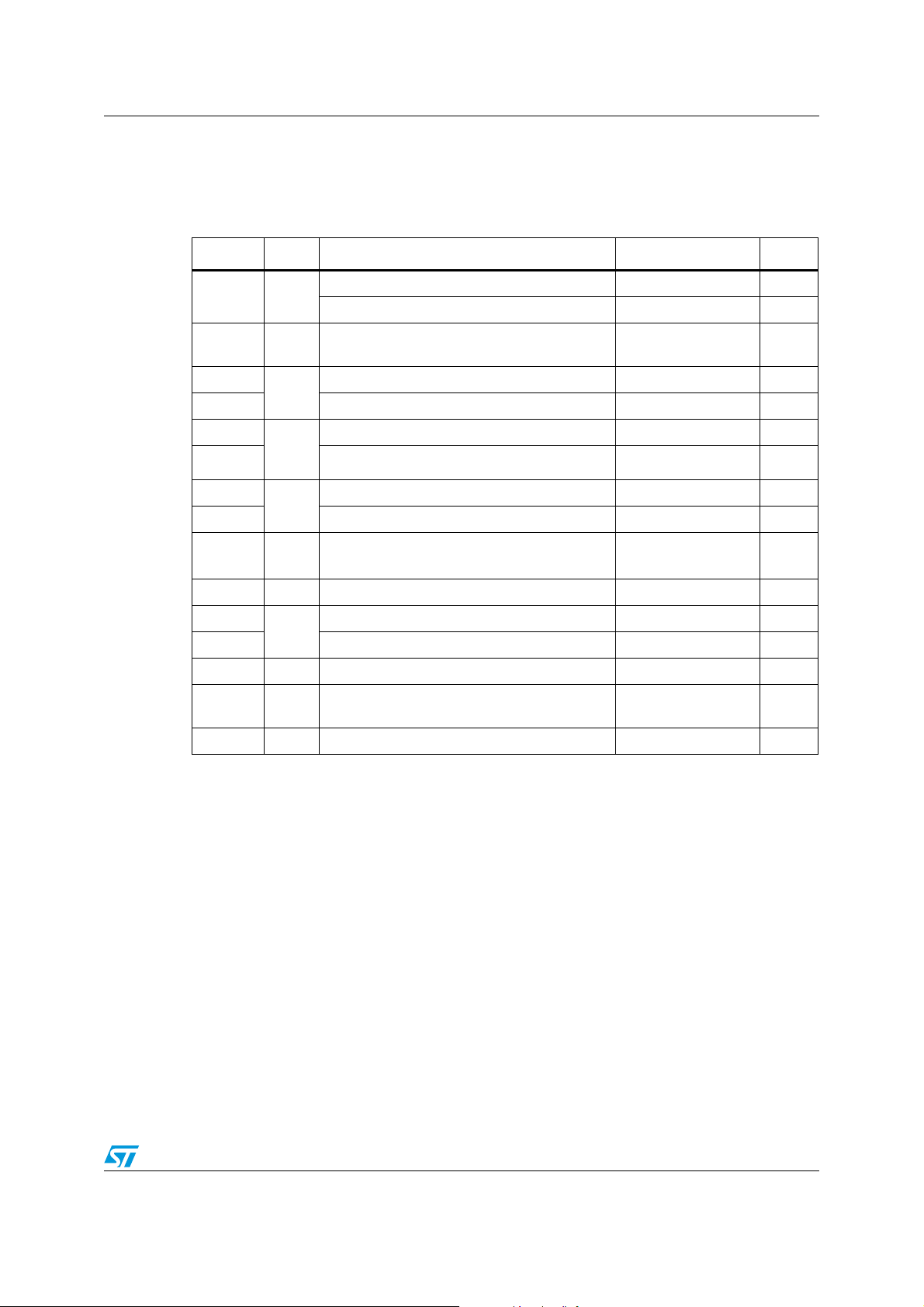
2 Pin connections
Figure 2. Pin connections (top view)
GND
O4
O3
VP
VC
V
S
VCP
O2
O1
GND 10
1
2
3
4
5
6
7
8
9
D95IN217
20
19
18
17
16
15
14
13
12
11
Table 3. Pin description
N# Pin name Function
Positive supply voltage. An internal circuit, monitoring the supply voltage,
6V
7V
CP
maintains the IC in OFF-state until VS reaches 9 V or when VS falls under
S
8.5 V. The diagnostic is availlable since V
Switch driver supply. To minimize the output drop voltage, a supply of about
10 V higher than VS is required. In order to use the built-in charge pump,
connect a filter capacitor from pin1 to pin. The suggested value assures a
fast transition and a low supply ripple even in worse condition. Using the
four channels contemporarily, values less than 68 nF have to be avoided.
GND
DIAG
R
OFF DELAY
ON DELAY
I4
I3
I2
I1
GND
= 5 V.
S
2, 3, 8, 9
1, 10,
11, 20
12,13,
14, 15
O1, O2,
O3, O
GND
, I2, I3, I
I
1
High side outputs. Four independently controlled outputs with built-in current
limitation.
4
Ground and power dissipating pins. These pins are connected to the bulk
ground of the IC, so are useful for heat dissipation.
Control inputs. Four independent control signals. The output is held OFF
until the voltage at the corresponding input pin reaches 1.35 V and is turned
4
OFF when the voltage at the pin goes below 1.15 V.
Programmable ON duration in short circuit. If an output is short circuited to
ground or carryng a current exceeding the limit, the output is turned OFF
16 ON DELAY
and the diagnostic activation are delayed. This procedure allows the driving
of hard surge current loads. The delay is programmed connecting a
capacitor (50 pF to 15 nF) versus ground with the internal time constant of
1.28 µs/pF. The function can be disabled short circuiting this pin to ground.
Programmable OFF duration in short circuit. After the short circuit or
overcurrent detection, the switch is held OFF before the next attempt to
switch on again. The delay is programmed connecting a capacitor (50 pF to
15 nF) versus ground with the internal time constant of 1.28 µs/pF. Short
17
OFF
DELAY
circuiting this pin to ground the OFF delay is 64 times the ON delay.
18 R
Asyncronous reset input. This active low input (with hysteresis), switch off all
the outputs independently from the input signal. By default it is biased low.
4/18
L6376 Pin connections
Table 3. Pin description (continued)
N# Pin name Function
Diagnostic output. This open drain output reports the IC working condition.
19 DIAG
5V
4V
The bad condition (as undervoltage, overcurrent, overtemperature) turns
the output low.
Pump oscillator voltage. At this pin is available the built-in circuitry to supply
the switch driver at about 10 V higher than V
capacitor across pin 4 and pin 5. The suggested value assures a fast
C
transition and a minimum output drop voltage even in worse condition.
. To use this feature, connect a
S
Using the four channels contemporarily, values less than 6.8 nF have to be
avoided.
Bootstrapped voltage. At this pin is available the 11 V oscillation for the
P
charge pump, at a typical frequency of 200 kHz.
5/18

Thermal characteristics L6376
3 Thermal characteristics
Table 4. Thermal data
Symbol Parameter Value Unit
R
R
thJA
thJC
Thermal resistance, junction to ambient
(see thermal characteristics)
Thermal resistance junction-case 1.5 °C/W
50 °C/W
Note: Additional data on the PowerSO-20 can be found in Application note AN668
6/18

L6376 Electrical characteristics
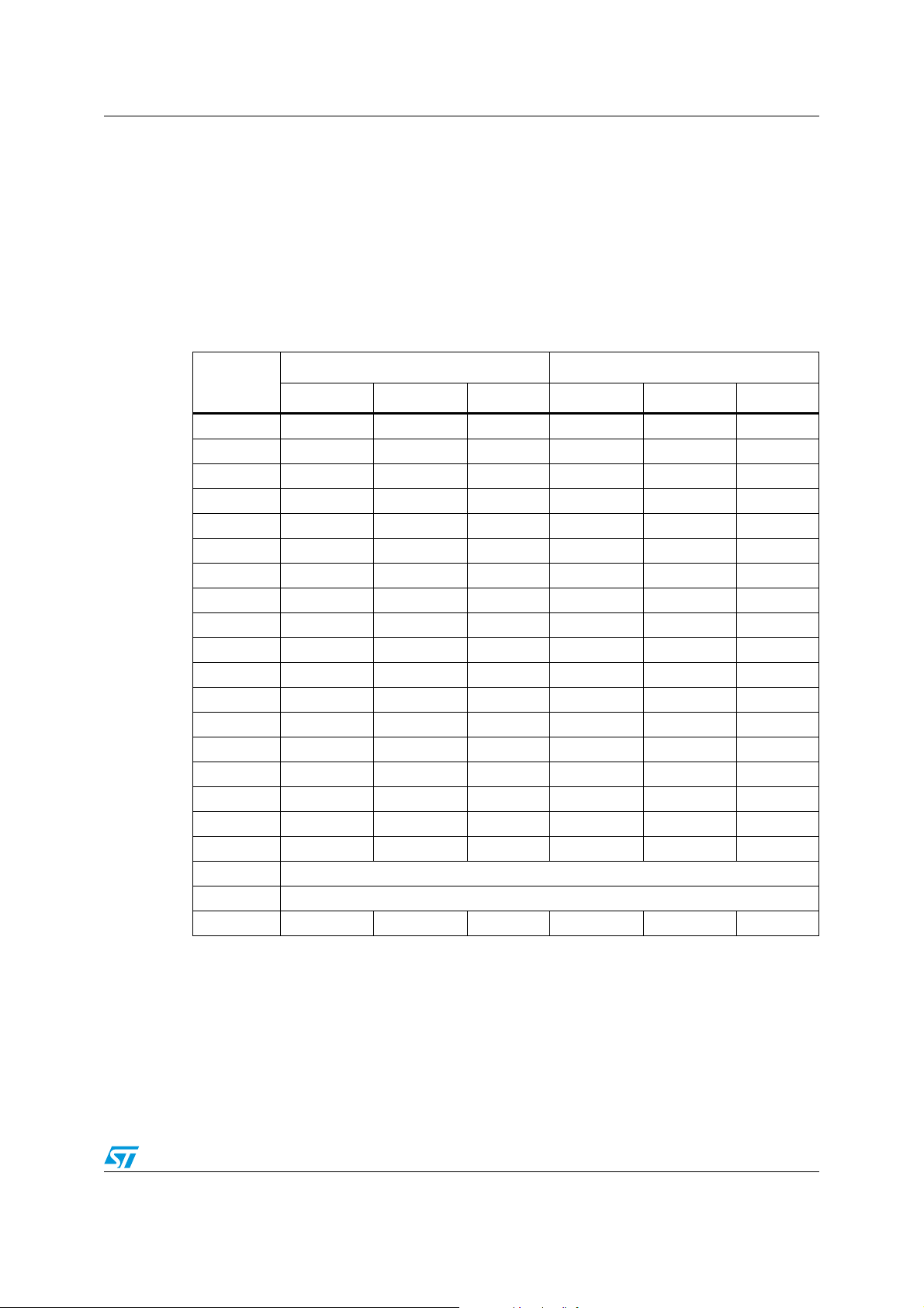
4 Electrical characteristics
Table 5. Electrical characteristcs
(V
= 24 V; TJ = -25 to 125 °C; unless otherwise specified.)
s
Symbol Pin# Parameter Test condition Min Typ Max Unit
DC operation
V
V
I
V
V
shys
I
qsc
V
V
bias
ihys
s
sth
il
ih
12,13,
14,15,
Supply voltage 9.5 24 35 V
UV upperthreshold 8.5 9 9.5 V
6
UV hysteresis 200 500 800 mV
Quiescent current Outputs ON, no load 3 5 mA
Input low level 0 0.8 V
Input high level 2 40 V
V
= 0 V -5 -1 0 µA
Input bias current
18
Input comparators
hysteresis
i
V
= 40 V 0 5 20 µA
i
100 200 400 mV
Θlim OVT upper threshold 150 °C
ΘH Threshold hysteresis 20 30 °C
= 9.5 to 35 V;
V
Short circuit current
I
2, 3, 8,
sc
9
s
= 2 Ω
R
l
= 500 mA;
I
out
TJ = 25 °C
0.65 0.9 1.2 A
320 500 mV
Output voltage drop
I
= 500 mA;
out
TJ = 125 °C
I
olk
V
cl
V
ol
I
dlkg
V
diag
I
dch
16, 17
Output leakage current Vo = 0 V; Vi < 0.8 V 100 µA
Internal voltage clamp
each output)
(V
s-Vo
Io = 100 mA
single pulsed
= 300 µs
T
p
Low state output voltage Vi = Vil; RL = ∞ 0.8 1.5 V
Diagnostic output leakage Diagnostic off 25 µA
19
Diagnostic output voltage
drop
= 5 mA 1.5 V
I
diag
Delay capacitors charge
current
460 640 mV
47 52 57 V
40 µA
7/18

Electrical characteristics L6376
Table 5. Electrical characteristcs (continued)
(V
= 24 V; TJ = -25 to 125 °C; unless otherwise specified.)
s
Symbol Pin# Parameter Test condition Min Typ Max Unit
AC operation
tr -t
2, 3, 8,
f
Rise or fall time
9
12 vs 9
13 vs 8
t
d
14 vs 3
Delay time 1 µs
15 vs 2
dV/dt
t
ON
t
OFF
f
max
2, 3, 8,
Slew rate
9
(Rise and fall edge)
On time during short
16
circuit condition
Off time during short
17
circuit condition
Maximum operating
frequency
Source drain ndmos diode
V
fsd
I
fp
t
rr
t
fr
Forward on voltage I
Forward peak current
Reverse recovery time
Forward recovery time 50 ns
3.8 µs
= 24 V; Rl = 47 Ω
V
s
Rl to ground
= 24 V; Rl = 47 Ω
V
s
Rl to ground
Rise
Fall
50 pF < C
< 15 nF 1.28 µs/pF
DON
3
4
5
7.6 710
pin 13 grounded 64 t
50 pF < C
< 15 nF 1.28 µs/pF
DOFF
25 kHz
= 500 mA 1 1.5 V
fsd
tp = 10 ms;
duty cycle = 20 %
= 500 mA;
I
fsd
dt = 25 A/ms
dI
fsd/
200 ns
1.5 A
V/µs
V/µs
ON
8/18

L6376 Electrical characteristics
Figure 3. Undervoltage comparator hysteresis
V
shys
Figure 4. Switching waveforms
V
in
50% 50%
t
d
V
out
50% 50%
10%
90% 90%
t
r
D94IN126A
V
sth
t
d
V
s
t
10%
t
f
D94IN127A
t
9/18

Overtemperature protection (OVT) L6376
5 Overtemperature protection (OVT)
If the chip temperature exceeds Θlim (measured in a central position in the chip) the chip
deactivates itself.
The following actions are taken:
● all the output stages are switched off;
● the signal DIAG is activated (active low).
Normal operation is resumed as soon as (typically after some seconds) the chip
temperature monitored goes back below Θ
lim-ΘH
.
The different thresholds with hysteretic behavior assure that no intermittent conditions can
be generated.
6 Undervoltage protection (UV)
The supply voltage is expected to range from 9.5 V to 35 V, even if its reference value is
considered to be 24 V. In this range the device operates correctly. Below 9.5 V the overall
system has to be considered not reliable. Consequently the supply voltage is monitored
continuously and a signal, called UV, is internally generated and used.
The signal is “on” as long as the supply voltage does not reach the upper internal threshold
of the Vs comparator V
. The UV signal disappears above V
sth
Once the UV signal has been removed, the supply voltage must decrease below the lower
threshold (i.e. V
The hysteresis V
sth-Vshys
shys
) before it is turned on again.
is provided to prevent intermittent operation of the device at low supply
voltages that may have a superimposed ripple around the average value.
The UV signal switches off the outputs, but has no effect on the creation of the reference
voltages for the internal comparators, nor on the continuous operation of the charge-pump
circuits.
7 Diagnostic logic
The situations that are monitored and signalled with the DIAG output pin are:
● current limit (OVC) in action; there are 4 individual current limiting circuits, one per each
output; they limit the current that can be sunk from each output, to a typical value of
800 mA, equal for all of them;
● under voltage (UV);
● over temperature protection (OVT).
The diagnostic signal is transmitted via an open drain output (for ease of wired-or
connection of several such signals) and a low level represents the presence of at least one
of the monitored conditions, mentioned above.
sth
.
10/18

L6376 Short circuit operation
8 Short circuit operation
In order to allow normal operation of the other inputs when one channel is in short cirtuit, an
innovative non dissipative over current protection (patent pending) is implemented in the
device.
Figure 5. Short circuit operation waveforms
OUTPUT
CURRENT
I
sc
I
out
Time
Time
DIAG
(active low)
t<t
ON
t
ON
t
OFF
Short CircuitShort Circuit
t
ON
t
OFF
D94IN105
In this way, the temperature of the device is kept enough low to prevent the intervention of
the thermal protection (in most of the cases) and so to avoid the shut down of the whole
device.
If a short circuit condition is present on one output, the current limiting circuit puts that
channel in linear mode — sourcing the ISC current (typically 800 mA) — for a time period
(t
) defined by an external capacitor (C
ON
connected to the ON DELAY pin).
DON
After that period, if the short circuit condition is still present the output is turned off for
another time period (t
) defined by a second external capacitor (C
OFF
connected to the
DOFF
OFF DELAY pin).
When also this period is expired:
● if the short circuit condition is still present the output stays on for the tON period and the
sequence starts again;
● if the short circuit condition is not present anymore the normal operation of the output is
resumed.
The t
ON
and t
periods are completely independent and can be set from 64 µs to 15 µs,
OFF
using external capacitors ranging from 50 pF to 15 nF (1.28 µs/pF).
If the OFF DELAY pin is tied to ground (i.e. the C
period is 64 times the t
period.
ON
capacitor is not used) the t
DOFF
OFF
time
The diagnostic output (DIAG) is active when the output is switched off, while it is not active
when the output is on (i.e. during the t
period) even if in that period a short circuit
ON
condition is present.
11/18

Programmable diagnostic delay L6376
Typical waveforms for short circuit operation are shown in Figure 5.
If both the ON DELAY and the OFF DELAY pins are grounded the non dissipative over
current protection is inhibited and the outputs in short circuit remain on until the thermal
shutdown switch OFF the whole device. In this case the short circuit condition is not
signalled by the DIAG pin (that continues to signal the under voltage and over temperature
conditions).
9 Programmable diagnostic delay
The current limiting circuits can be requested to perform even in absence of a real fault
condition, for a short period, if the load is of capacitive nature or if it is a filament lamp (that
exhibits a very low resistance during the initial heating phase).
To avoid the forwarding of misleading — i.e. short diagnostic pulses in coincidence with the
intervention of the current limiting circuits when operating on capacitive loads — the
activation of the diagnostic can be delayed with respect to the intervention of one of the
current limiting circuits.
This delay can be defined by an external capacitor (C
DELAY pin and ground.
10 Reset input
An external reset input R (pin 18) is provided to simultaneously switch OFF all the outputs:
this signal (active low) is in effect an asynchronous reset that keeps the outputs low
independently from the input signals. For example, this reset input can be used by the CPU
to keep the outputs low after a fault condition (signaled by the DIAG pin).
) connected between the ON
DON
12/18

L6376 Demagnetization of inductive loads
11 Demagnetization of inductive loads
The device has four internal clamping diodes able to demagnetize inductive loads.
The limitation is the peak power dissipation of the packages, so — if the loads are big or if
there is the possibility to demagnetize more loads contemporarly — it is necessary to use
external demagnetization circuits.
In Figure 7 and Figure 8 are shown two topologies for the demagnetization versus ground
and versus V
The breakdown voltage of the external device (V
minimum internal clamping voltage (V
Figure 6. Input comparator hysteresis
.
S
) must be chosen considering the
) and the maximum supply voltage (VS).
cl
V
V
out
s
100mV
Z
100mV
1.25V
D94IN131
Figure 7. External demagnetization circuit (versus ground)
V
S
V
CP
DRIVER
UV
SHORT CIRCUIT
CONTROL
R
S
CURRENT
LIMIT
D94IN109
OVC
VZ < V
cl (min)
- V
S (max)
O
1
O
2
O
3
O
4
V
i
V
Z
13/18

Demagnetization of inductive loads L6376
)
Figure 8. External demagnetization circuit (versus VS)
V
S
V
V
CP
DRIVER
UV
SHORT CIRCUIT
CONTROL
R
S
CURRENT
LIMIT
OVC
O
1
O
2
O
3
O
4
S
V
Z
D94IN110A
V
S (max)
< VZ < V
cl (min
14/18
L6376 Package mechanical data
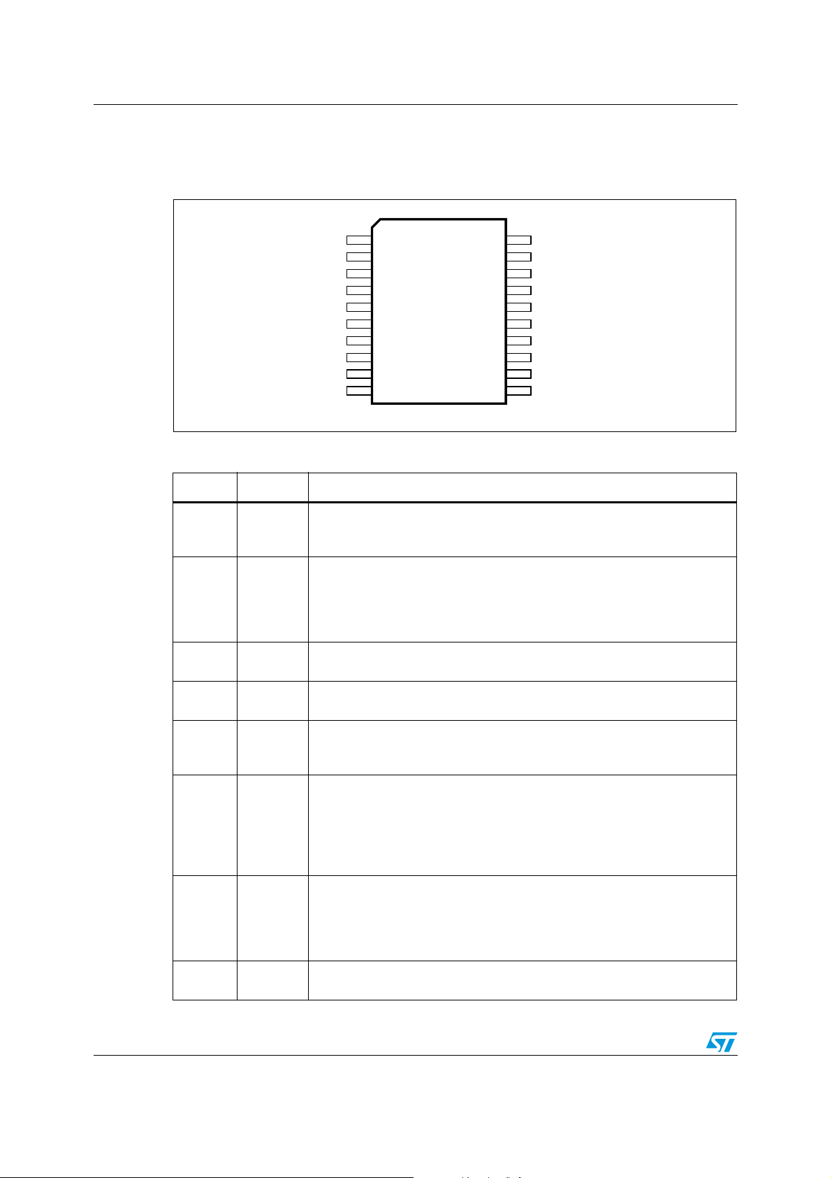
12 Package mechanical data
In order to meet environmental requirements, ST offers these devices in ECOPACK®
packages. These packages have a lead-free second level interconnect . The category of
second level interconnect is marked on the package and on the inner box label, in
compliance with JEDEC Standard JESD97. The maximum ratings related to soldering
conditions are also marked on the inner box label. ECOPACK is an ST trademark.
ECOPACK specifications are available at: www.st.com
Table 6. PowerSO-20 mechanical data
mm inch
Dim.
A 3.6 0.142
a1 0.1 0.3 0.004 0.012
a2 3.3 0.130
a3 0 0.1 0.000 0.004
b 0.4 0.53 0.016 0.021
c 0.23 0.32 0.009 0.013
D (1) 15.8 16 0.622 0.630
D1 (2) 9.4 9.8 0.370 0.386
E 13.9 14.5 0.547 0.570
e 1.27 0.050
e3 11.43 0.450
E1 (1) 10.9 11.1 0.429 0.437
E2 2.9 0.114
E3 5.8 6.2 0.228 0.244
G 0 0.1 0.000 0.004
H 15.5 15.9 0.610 0.626
h 1.1 0.043
L 0.8 1.1 0.031 0.043
N 8°(typ.)
S 8°(max. )
T 10 0.394
Min Typ Max Min Typ Max
15/18

Package mechanical data L6376
Figure 9. Package dimensions
DETAIL B
R
c
a1
E
lead
DETAIL A
NN
a2
A
b
DETAIL A
e
e3
H
E2
h x 45˚
D
1120
E1
T
110
PSO20MEC
a3
Gage Plane
BOTTOM VIEW
DETAIL B
0.35
S
D1
slug
- C -
L
SEATING PLANE
GC
(COPLANARITY)
E3
0056635 I
16/18

L6376 Revision history
13 Revision history
Table 7. Document revision history
Date Revision Changes
September 2003 5 First issue in EDOCS dms.
03-Mar-2008 6 Modified: Removed obsolete package DIP-20
17/18

L6376
Please Read Carefully:
Information in this document is provided solely in connection with ST products. STMicroelectronics NV and its subsidiaries (“ST”) reserve the
right to make changes, corrections, modifications or improvements, to this document, and the products and services described herein at any
time, without notice.
All ST products are sold pursuant to ST’s terms and conditions of sale.
Purchasers are solely responsible for the choice, selection and use of the ST products and services described herein, and ST assumes no
liability whatsoever relating to the choice, selection or use of the ST products and services described herein.
No license, express or implied, by estoppel or otherwise, to any intellectual property rights is granted under this document. If any part of this
document refers to any third party products or services it shall not be deemed a license grant by ST for the use of such third party products
or services, or any intellectual property contained therein or considered as a warranty covering the use in any manner whatsoever of such
third party products or services or any intellectual property contained therein.
UNLESS OTHERWISE SET FORTH IN ST’S TERMS AND CONDITIONS OF SALE ST DISCLAIMS ANY EXPRESS OR IMPLIED
WARRANTY WITH RESPECT TO THE USE AND/OR SALE OF ST PRODUCTS INCLUDING WITHOUT LIMITATION IMPLIED
WARRANTIES OF MERCHANTABILITY, FITNESS FOR A PARTICULAR PURPOSE (AND THEIR EQUIVALENTS UNDER THE LAWS
OF ANY JURISDICTION), OR INFRINGEMENT OF ANY PATENT, COPYRIGHT OR OTHER INTELLECTUAL PROPERTY RIGHT.
UNLESS EXPRESSLY APPROVED IN WRITING BY AN AUTHORIZED ST REPRESENTATIVE, ST PRODUCTS ARE NOT
RECOMMENDED, AUTHORIZED OR WARRANTED FOR USE IN MILITARY, AIR CRAFT, SPACE, LIFE SAVING, OR LIFE SUSTAINING
APPLICATIONS, NOR IN PRODUCTS OR SYSTEMS WHERE FAILURE OR MALFUNCTION MAY RESULT IN PERSONAL INJURY,
DEATH, OR SEVERE PROPERTY OR ENVIRONMENTAL DAMAGE. ST PRODUCTS WHICH ARE NOT SPECIFIED AS "AUTOMOTIVE
GRADE" MAY ONLY BE USED IN AUTOMOTIVE APPLICATIONS AT USER’S OWN RISK.
Resale of ST products with provisions different from the statements and/or technical features set forth in this document shall immediately void
any warranty granted by ST for the ST product or service described herein and shall not create or extend in any manner whatsoever, any
liability of ST.
ST and the ST logo are trademarks or registered trademarks of ST in various countries.
Information in this document supersedes and replaces all information previously supplied.
The ST logo is a registered trademark of STMicroelectronics. All other names are the property of their respective owners.
© 2008 STMicroelectronics - All rights reserved
STMicroelectronics group of companies
Australia - Belgium - Brazil - Canada - China - Czech Republic - Finland - France - Germany - Hong Kong - India - Israel - Italy - Japan -
Malaysia - Malta - Morocco - Singapore - Spain - Sweden - Switzerland - United Kingdom - United States of America
www.st.com
18/18
 Loading...