

Page 1
0.5 A high-side driver intelligent power switch
Features
■ 0.5 A output current
■ 8 V to 35 V supply voltage range
■ Internal current limiting
■ Thermal shutdown
■ Open ground protection
■ Internal negative voltage clamping for fast
demagnetization
■ Differential inputs with large common mode
range and threshold hysteresis
■ Undervoltage lockout with hysteresis
■ Open load detection
■ Two diagnostic outputs
■ Output status LED driver
■ Non-dissipative short-circuit protection
■ Immunity against burst transient
(IEC 61000-4-4)
■ ESD protection (human body model ±2 kV)
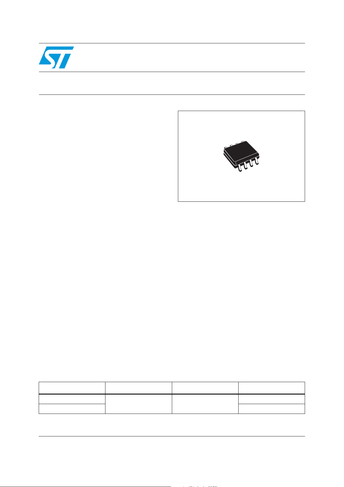
L6375S
SO-8
Description
The L6375S is a monolithic intelligent power
switch in BCDmultipower technology, for driving
inductive or resistive loads with controlled output
voltage slew rate and short-circuit protection.
An internal clamping diode enables the fast
demagnetization of inductive loads. Diagnostics
for CPU feedback and extensive use of electrical
protection make this device extremely rugged and
specially suitable for industrial automation
applications.
Table 1. Device summary
December 2011 Doc ID 12603 Rev 8 1/17
Order codes Op. temp. range Package Packaging
L6375S
Tu b e
-25 to +125 °C SO-8
L6375STR Tape and reel
www.st.com
17
Page 2

Contents L6375S
Contents
1 Block diagram and pin description . . . . . . . . . . . . . . . . . . . . . . . . . . . . . 3
1.1 Pin description . . . . . . . . . . . . . . . . . . . . . . . . . . . . . . . . . . . . . . . . . . . . . . 4
2 Electrical specifications . . . . . . . . . . . . . . . . . . . . . . . . . . . . . . . . . . . . . . 5
2.1 Absolute maximum ratings . . . . . . . . . . . . . . . . . . . . . . . . . . . . . . . . . . . . . 5
2.2 Thermal data . . . . . . . . . . . . . . . . . . . . . . . . . . . . . . . . . . . . . . . . . . . . . . . 5
2.3 Electrical characteristics . . . . . . . . . . . . . . . . . . . . . . . . . . . . . . . . . . . . . . . 6
2.4 Switching waveform . . . . . . . . . . . . . . . . . . . . . . . . . . . . . . . . . . . . . . . . . . 8
2.5 Input section . . . . . . . . . . . . . . . . . . . . . . . . . . . . . . . . . . . . . . . . . . . . . . . . 8
2.6 Overtemperature protection (OVT) . . . . . . . . . . . . . . . . . . . . . . . . . . . . . . . 8
2.7 Undervoltage protection (UV) . . . . . . . . . . . . . . . . . . . . . . . . . . . . . . . . . . . 8
2.8 Overcurrent operation . . . . . . . . . . . . . . . . . . . . . . . . . . . . . . . . . . . . . . . . 9
2.9 Diagnostic logic . . . . . . . . . . . . . . . . . . . . . . . . . . . . . . . . . . . . . . . . . . . . 10
2.10 Demagnetization of inductive loads . . . . . . . . . . . . . . . . . . . . . . . . . . . . . 10
2.11 Diagnostic truth table . . . . . . . . . . . . . . . . . . . . . . . . . . . . . . . . . . . . . . . . 10
3 Application circuits . . . . . . . . . . . . . . . . . . . . . . . . . . . . . . . . . . . . . . . . . 11
4 Package mechanical data . . . . . . . . . . . . . . . . . . . . . . . . . . . . . . . . . . . . 13
5 Revision history . . . . . . . . . . . . . . . . . . . . . . . . . . . . . . . . . . . . . . . . . . . 16
2/17 Doc ID 12603 Rev 8
Page 3
L6375S Block diagram and pin description
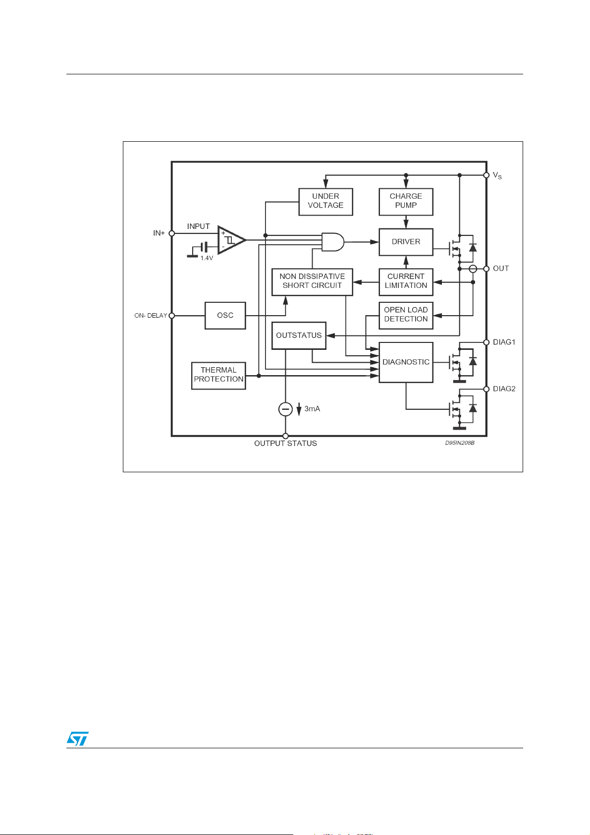
1 Block diagram and pin description
Figure 1. Block diagram
Doc ID 12603 Rev 8 3/17
Page 4
Block diagram and pin description L6375S
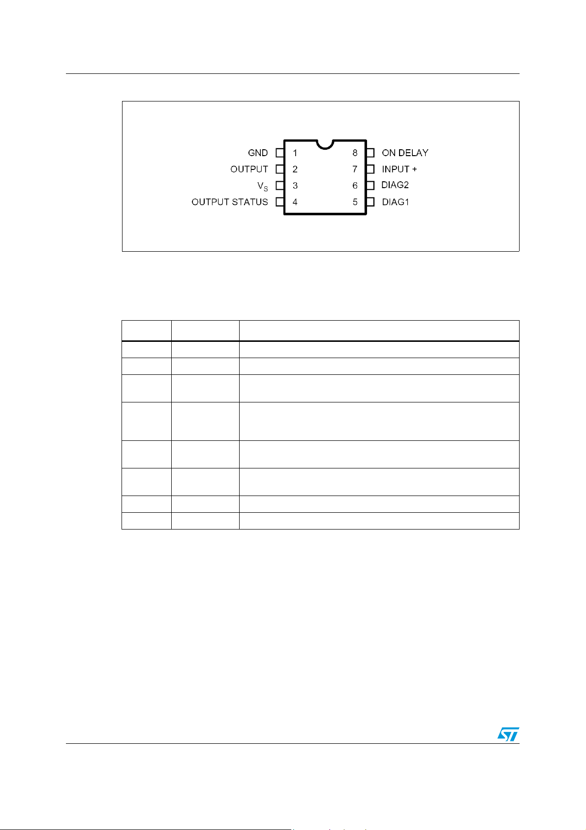
Figure 2. Pin connection (top view)
SO-8
1.1 Pin description
Table 2. Pin description
Pin n° Pin name Function
1 GND Ground
2 OUT High side output with built-in current limitation
3V
S
4 Output status
5 DIAG1
Supply voltage input; the value of the supply voltage is monitored to
detect undervoltage condition
This current source output is capable of driving an LED to signal the
status of the output pin. The pin is active (source current) when the
output pin is considered high (see Figure 4)
DIAGNOSTIC 1 output. This open drain reports the IC working
conditions (see Table 6: Diagnostic truth table)
6 DIAG2
DIAGNOSTIC 2 output. This open drain reports the IC working
conditions (see Table 6: Diagnostic truth table)
7 IN+ Comparator inverting input
8 ON-DELAY Programmable ON time interval duration during short-circuit operation
4/17 Doc ID 12603 Rev 8
Page 5
L6375S Electrical specifications
2 Electrical specifications
2.1 Absolute maximum ratings
Table 3. Absolute maximum ratings
Symbol Parameter Value Unit
V
Supply voltage (tw < 10 ms) 50 V
S
V
Supply voltage (DC) 40 V
S
V
-V
Supply to output differential voltage Internally limited V
out
S
od Externally forced voltage -0.3 to 7 V
V
od Externally forced current ±1 mA
I
I
out Output current (see also Isc) Internally limited A
Output voltage Internally limited V
V
out
P
TOT
V
diag
I
diag
I
Vi Input voltage -10 to V
Top Ambient temperature, operating range -25 to 85 °C
Power dissipation Internally limited W
External voltage -0.3 to 40 V
Externally forced current -10 to 10 mA
i Input current 20 mA
+0.3 V
S
T
J
STG Storage temperature -55 to 150 °C
T
E
I
2.2 Thermal data
Table 4. Thermal data
Symbol Parameter Value Unit
R
thJA
R
thJP
1. When mounted on a standard single-sided FR-4 board with 0.5 cm2 of Cu (at least 35 μm thick) connected
to all V
Junction temperature, operating range
(see Section 2.6)
-25 to 125 °C
Energy inductive load TJ = 85 °C 200 mJ
Thermal resistance junction-ambient max.
100
(1)
Thermal resistance junction-pins max. 15 °C/W
pins. Horizontal mounting and no artificial air flow.
CC
°C/W
Doc ID 12603 Rev 8 5/17
Page 6
Electrical specifications L6375S
2.3 Electrical characteristics
VS = 24 V; TJ = –25 to +125 °C, unless otherwise specified.
Table 5. Electrical characteristics
Symbol Parameter Test condition Min. Typ. Max. Unit
V
V
V
V
V
V
I
V
V
I
V
V
V
dch
Supply voltage for valid
smin
diagnostic
Operative supply voltage 8 24 35 V
S
Undervoltage threshold 1 7 7.5 8 V
sth1
Undervoltage threshold 2 6.5 7 7.5 V
sth2
Undervoltage hysteresis 300 500 700 mV
shys
I
Quiescent current Output open 800 μA
q
Quiescent current Output ON 1.6 mA
qo
Input threshold voltage 0.8 1.3 2 V
ith
Input threshold hysteresis 50 400 mV
iths
Input low level voltage -7 0.8 V
il
Input high level voltage V
ih
Input high level voltage V
ih
Input bias current Vi = -7 to 15 V -250 250 μA
I
ib
Delay capacitor charging
current
Output voltage drop
don
I
= > 0.5 mA;
diag
V
= 1.5 V;
diag
< 18 V 2 V
S
> 18 V 2 15 V
S
ON DELAY pin shorted to
ground
Iout = 500 mA T
= 125 °C
T
J
= 25 °C
J
Iout =625 mA TJ = 25 °C
TJ= 125 °C
4 35 V
- 3 V
S
2.5 μA
200
320
250
400
280
440
350
550
mV
mV
mV
mV
I
V
V
I
I
V
V
V
ohys
I
osd
Output leakage current Vi = LOW; V
olk
Output low state voltage Vi = HIGH; pin floating 0.8 1.5 V
ol
Internal voltage clamp
cl
V
-V
(
Short-circuit output current VS = 8 to 35 V; Rl = 2 Ω; 0.75 1.1 1.5 A
sc
Open load detection current Vi = Vih; TA= 0 to +85 °C 1 3 6 mA
old
Output status threshold 1
oth1
voltage
Output status threshold 2
oth2
voltage
Output status threshold
hysteresis
)
out
S
Output status source current V
6/17 Doc ID 12603 Rev 8
=0 100 μA
out
I
= 200 mA
o
single pulsed = 300 ms
48 53 58 V
4.5 5 5.5 V
4 4.5 5 V
300 500 700 mV
> V
out
; VOS = 2.5 V 2 4 mA
oth1
Page 7

L6375S Electrical specifications
Table 5. Electrical characteristics (continued)
Symbol Parameter Test condition Min. Typ. Max. Unit
Active output status driver drop
V
osd
voltage
Output status driver leakage
I
oslk
current
Diagnostic drop voltage
V
dgl
dglk Diagnostic leakage current
I
T
T
Overtemperature upper
max
threshold
Overtemperature hysteresis 20 °C
hys
– VOS; IOS = 2 mA
V
S
TA = 0 to +85 °C
V
out
< V
; VOS = 0 V
oth2
VS = 18 to 35 V
D1 / D2 = L; I
D1 / D2 = L; I
diag
diag
D1 / D2 = H; 0 < V
= 15.6 to 35 V
V
S
= 0.5 mA
= 3 mA
< VS
dg
1.5 3 V
25 µA
40
250
5 μA
150 °C
AC operation (pin numbering referred to Minidip package)
V
= 24 V; Rl =70 Ω Rl to
-tr Rise or fall time
t
r
Delay time
t
d
S
ground
V
= 24 V; Rl =70 Ω Rl to
S
ground
20 μs
5 μs
dV/dt Slew rate (rise and fall edge) 0.7 1 1.5 V/μs
ON time during short-circuit
t
ON
t
OFF
f
max
condition
OFF time during short-circuit
condition
Maximum operating frequency 25 KHz
50 pF < C
< 2 nF 1.28 μs/pF
DON
64 t
Source drain NDMOS diode
mV
mV
ON
V
Forward ON voltage @ Ifsd = 625 mA 1 1.5 V
f
Forward peak voltage t = 10 ms; d = 20% 2 A
I
fD
Reverse recovery time If = 625 mA di/dt = 25 A/ms 200 ns
t
rr
t
Forward recovery time 50 ns
fr
Doc ID 12603 Rev 8 7/17
Page 8
Electrical specifications L6375S
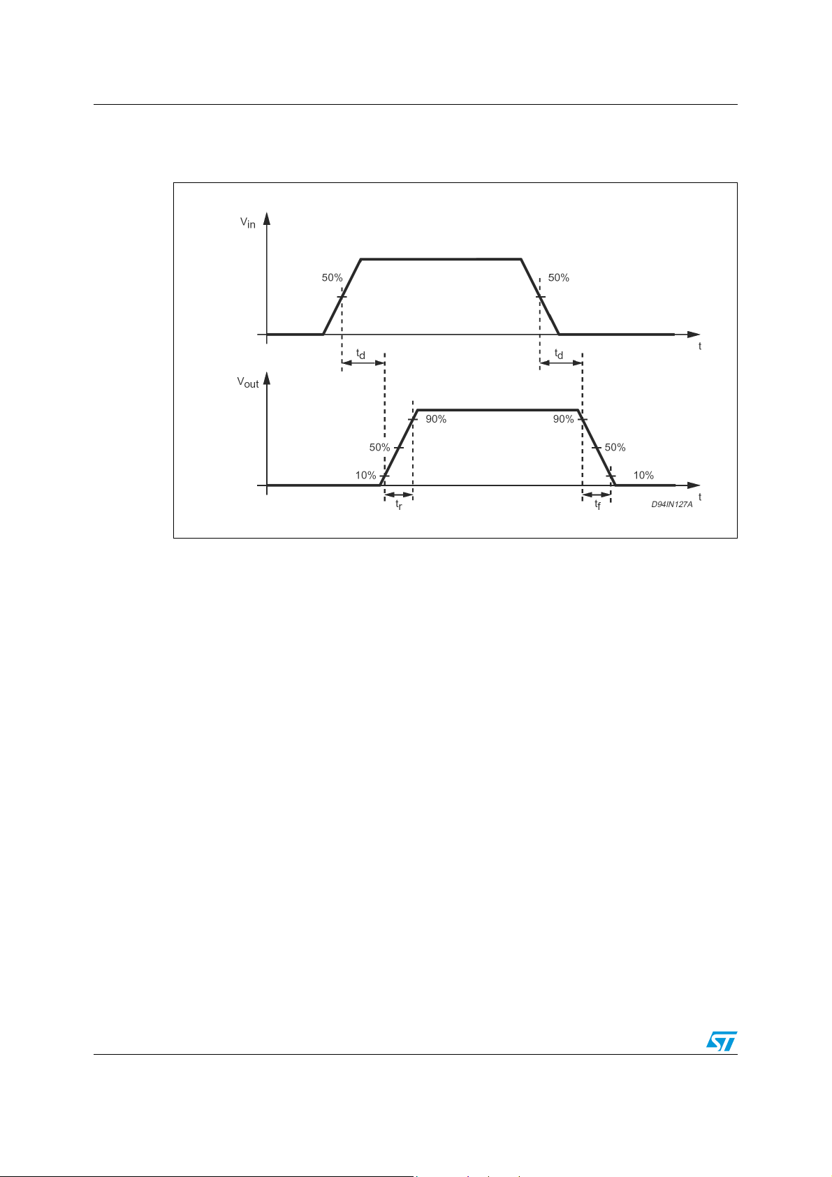
2.4 Switching waveform
Figure 3. Switching waveform
2.5 Input section
An single ended input TTL/CMOS compatible with a wide voltage range and high noise
immunity (thanks to a built-in hysteresis) is available.
2.6 Overtemperature protection (OVT)
An on-chip overtemperature protection provides excellent protection of the device in
extreme conditions. Whenever the temperature, measured on a central portion of the chip,
exceeds T
= 150 °C (typical value), the device is shut off, and the DIAG2 output goes
max
LOW. Normal operation is resumed as the chip temperature (normally after a few seconds)
falls below T
max
- T
= 130 °C (typical value). The hysteresis avoids that an intermittent
hys
behavior takes place.
2.7 Undervoltage protection (UV)
The supply voltage is expected to range from 8 to 35 V. In this range the device operates
correctly. To avoid any malfunctioning the supply voltage is continuously monitored to
provide an undervoltage protection. As V
Figure 1) the output Power MOSFET is switched off and DIAG1 and DIAG2 (see
Section 2.11). Normal operation is resumed as soon as V
behavior prevents intermittent operation at low supply voltage.
falls below V
S
sth-Vshys
exceeds V
S
(typically 7.5 V, see
. The hysteretic
sth
8/17 Doc ID 12603 Rev 8
Page 9

L6375S Electrical specifications
2.8 Overcurrent operation
In order to implement a short-circuit protection the output Power MOSFET is driven in linear
mode to limit the output current to the I
to the I
value) lasts for a Ton time interval, that can be set by means of a capacitor (C
sc
connected to the ON DELAY pin according to the following formula:
T
= 1.28 μsec/pF
on
for
(1.1 A typical value). This condition (current limited
sc
don
)
50 pF< C
After the T
< 2 nF
don
interval has expired the output Power MOSFET is switched off for the T
on
off
time
interval with:
T
= 64 ·Ton.
off
When also the T
interval has expired, the output Power MOSFET is switched ON. At this
off
point in time two conditions may occur
a) The overload is still present, and then the output Power MOSFET is again driven
in linear mode (limiting the output current to I
) for another Ton, starting a new
sc
cycle, or
b) the overload condition is removed, and the output Power MOSFET is no longer
driven in linear mode. All these occurrences are presented on the DIAG2 pin
(see Figure 2).
This unique feature is called non-dissipative short-circuit protection and it ensures a very
safe operation even in permanent overload conditions. Note that choosing the most
appropriate value for the T
interval (i.e. the value of the C
on
capacitor) a delay (the Ton
don
itself) prevents misleading short-circuit information being presented on the DIAG2 output,
when driving capacitive loads (that acts as a short-circuit in the very beginning) or an
incandescent lamp (a cold filament has a very low resistive value). The non-dissipative
short-circuit protection can be disabled (keeping T
limited to I
Figure 4. Non-dissipative short-circuit protection operation
, and diagnostic disabled) simply shorting to ground the ON DELAY pin.
sc
= 0 but with the output current still
on
Doc ID 12603 Rev 8 9/17
Page 10
Electrical specifications L6375S
2.9 Diagnostic logic
The operating conditions of the device are permanently monitored and the following
occurrences are signalled via the DIAG1/DIAG2 open-drain output pins, see Ta b le 6 :
Diagnostic truth table.
● Short-circuit vs. ground
● Short-circuit vs. VS
● Undervoltage (UV)
● Overtemperature (OVT)
● Open load, if the output current is less than 3 mA (typical value).
2.10 Demagnetization of inductive loads
An internal Zener diode, limiting the voltage across the Power MOSFET to between 50 and
60 V (V
), provides safe and fast demagnetization of inductive loads without external
cl
clamping devices. The maximum energy that can be absorbed from an inductive load is
specified as 200 mJ (at T
= 85 °C).
J
2.11 Diagnostic truth table
Table 6. Diagnostic truth table
Diagnostic conditions Input Output Diag1 Diag2
Normal operation
Open load condition (I
Short to V
S
Short-circuit to ground (I
o
< I
O
)
old
= Isc)
(1)
(pin ON-DELAY grounded)
Output DMOS open
Overtemperature
Supply undervoltage (V
1. A cold lamp filament, or a capacitive load may activate the current limiting circuit of the IPS, when the IPS
is initially turned on.
S
< V
sth2
)
L
H
L
H
L
H
H
L
L
H
L
H
L
H
L
H
L
H
H
H
X
L
L
L
L
L
L
L
H
H
H
L
L
L
H
H
H
L
H
H
L
L
H
H
H
H
H
H
H
H
H
H
L
L
L
L
10/17 Doc ID 12603 Rev 8
Page 11
L6375S Application circuits
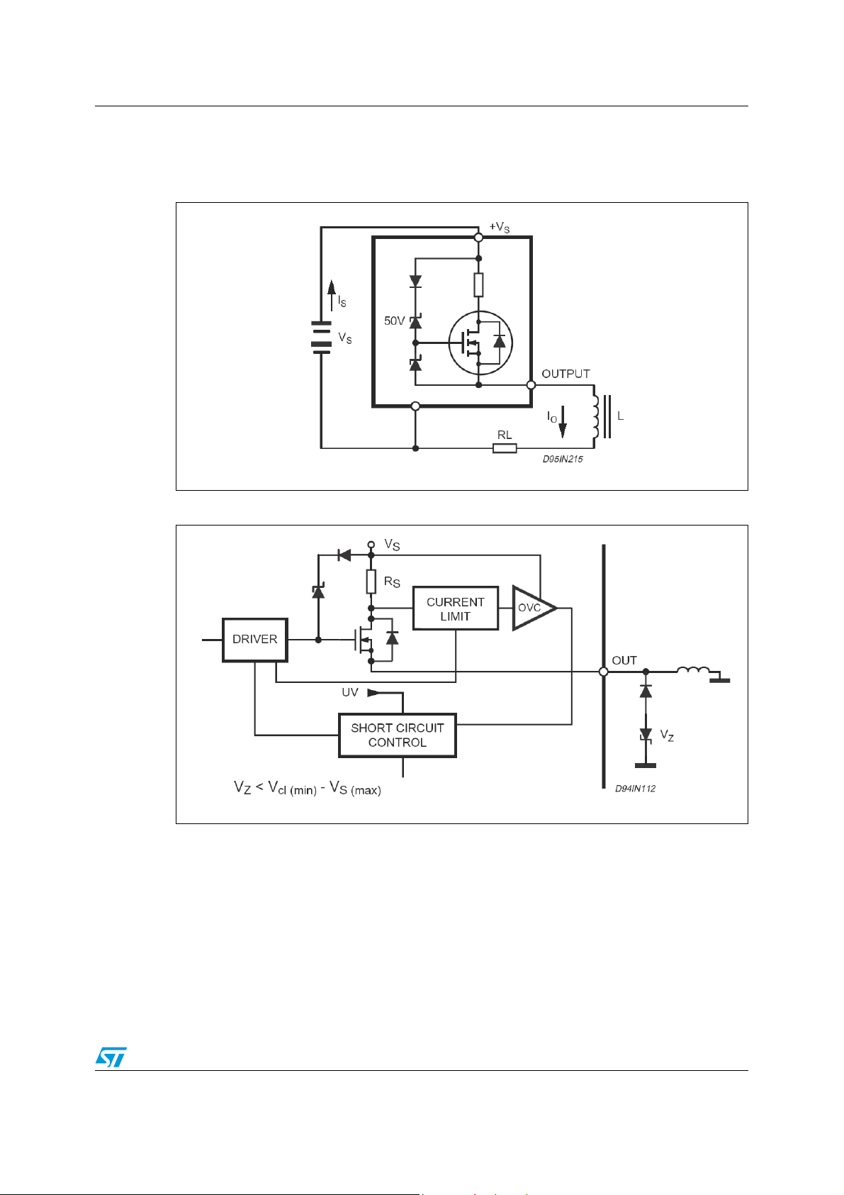
3 Application circuits
Figure 5. Inductive load equivalent circuit
Figure 6. External demagnetization circuit (vs. ground)
Doc ID 12603 Rev 8 11/17
Page 12

Application circuits L6375S
Figure 7. External demagnetization circuit (vs. VS)
Figure 8. Application schematic
ON-DELAY
(IEC 61000-4-5)
(IEC 61000-4-6)
12/17 Doc ID 12603 Rev 8
Page 13

L6375S Package mechanical data
4 Package mechanical data
In order to meet environmental requirements, ST offers these devices in different grades of
ECOPACK
®
packages, depending on their level of environmental compliance. ECOPACK
specifications, grade definitions and product status are available at: www.st.com.
ECOPACK is an ST trademark.
Doc ID 12603 Rev 8 13/17
Page 14

Package mechanical data L6375S
Table 7. SO-8 mechanical data
mm inch
Dim.
Min. Typ. Max. Min. Typ. Max.
A 1.75 0.068
a1 0.1 0.25 0.003 0.009
a2 1.65 0.064
a3 0.65 0.85 0.025 0.033
b 0.35 0.48 0.013 0.018
b1 0.19 0.25 0.007 0.010
C 0.25 0.5 0.010 0.019
c1 45 (typ.)
D 4.8 5.0 0.188 0.196
E 5.8 6.2 0.228 0.244
e 1.27 0.050
e3 3.81 0.150
F 3.8 4.0 0.14 0.157
L 0.4 1.27 0.015 0.050
M 0.6 0.023
S 8º (max.)
Figure 9. Package dimensions
14/17 Doc ID 12603 Rev 8
Page 15

L6375S Package mechanical data
Figure 10. SO-8 tape and reel information
Doc ID 12603 Rev 8 15/17
Page 16

Revision history L6375S
5 Revision history
Table 8. Revision history
Date Revision Changes
18-Sep-2006 1 Initial release
19-Jun-2007 2 Truth table updated
05-Jul-2007 3 Typo in Table 5 on page 6
16-Jul-2007 4 Pin out updated
15-Oct-2007 5 Updated Table 4 on page 5
29-Jun-2009 6 Updated Table 5 on page 6
12-Mar-2010 7 Updated Table 5 on page 6
20-Dec-2011 8 Updated Table 5 on page 6
16/17 Doc ID 12603 Rev 8
Page 17

L6375S
Please Read Carefully:
Information in this document is provided solely in connection with ST products. STMicroelectronics NV and its subsidiaries (“ST”) reserve the
right to make changes, corrections, modifications or improvements, to this document, and the products and services described herein at any
time, without notice.
All ST products are sold pursuant to ST’s terms and conditions of sale.
Purchasers are solely responsible for the choice, selection and use of the ST products and services described herein, and ST assumes no
liability whatsoever relating to the choice, selection or use of the ST products and services described herein.
No license, express or implied, by estoppel or otherwise, to any intellectual property rights is granted under this document. If any part of this
document refers to any third party products or services it shall not be deemed a license grant by ST for the use of such third party products
or services, or any intellectual property contained therein or considered as a warranty covering the use in any manner whatsoever of such
third party products or services or any intellectual property contained therein.
UNLESS OTHERWISE SET FORTH IN ST’S TERMS AND CONDITIONS OF SALE ST DISCLAIMS ANY EXPRESS OR IMPLIED
WARRANTY WITH RESPECT TO THE USE AND/OR SALE OF ST PRODUCTS INCLUDING WITHOUT LIMITATION IMPLIED
WARRANTIES OF MERCHANTABILITY, FITNESS FOR A PARTICULAR PURPOSE (AND THEIR EQUIVALENTS UNDER THE LAWS
OF ANY JURISDICTION), OR INFRINGEMENT OF ANY PATENT, COPYRIGHT OR OTHER INTELLECTUAL PROPERTY RIGHT.
UNLESS EXPRESSLY APPROVED IN WRITING BY TWO AUTHORIZED ST REPRESENTATIVES, ST PRODUCTS ARE NOT
RECOMMENDED, AUTHORIZED OR WARRANTED FOR USE IN MILITARY, AIR CRAFT, SPACE, LIFE SAVING, OR LIFE SUSTAINING
APPLICATIONS, NOR IN PRODUCTS OR SYSTEMS WHERE FAILURE OR MALFUNCTION MAY RESULT IN PERSONAL INJURY,
DEATH, OR SEVERE PROPERTY OR ENVIRONMENTAL DAMAGE. ST PRODUCTS WHICH ARE NOT SPECIFIED AS "AUTOMOTIVE
GRADE" MAY ONLY BE USED IN AUTOMOTIVE APPLICATIONS AT USER’S OWN RISK.
Resale of ST products with provisions different from the statements and/or technical features set forth in this document shall immediately void
any warranty granted by ST for the ST product or service described herein and shall not create or extend in any manner whatsoever, any
liability of ST.
ST and the ST logo are trademarks or registered trademarks of ST in various countries.
Information in this document supersedes and replaces all information previously supplied.
The ST logo is a registered trademark of STMicroelectronics. All other names are the property of their respective owners.
© 2011 STMicroelectronics - All rights reserved
Australia - Belgium - Brazil - Canada - China - Czech Republic - Finland - France - Germany - Hong Kong - India - Israel - Italy - Japan -
STMicroelectronics group of companies
Malaysia - Malta - Morocco - Philippines - Singapore - Spain - Sweden - Switzerland - United Kingdom - United States of America
www.st.com
Doc ID 12603 Rev 8 17/17
 Loading...