


6 / 4 CHANNEL VOLTAGE SENSE GMR PREAMPLIFIER
■
Power Supplies +5Vdc, -5Vdc
■
Current bias or voltage bias (selectable) /
Differential Voltage Sense architecture
■
6 or 4 channel versions
■
38-pin TSSOP package (for either 6 or 4
channels)
■
Internal reference Resistor for read and write
currents
■
Read channel -3dB bandwidth > 400MHz
(Rmr=50 ohm no interconnect)
■
Input equivalent preamplifier voltage noise
0.5nV/rtHz nominal
■
Input equivalent MR bias current noise 10 pA/
rtHz nominal
■
MR bias current programmable (5 bit DAC) 1.5-
7.0mA nominal MR bias voltage programmable
(5 bit DAC) 65-335mV nominal
■
Programmable gain (100V/V, 150, 200 and
250V/V) and read bandwidth
■
Write frequency up to 300 MHz (Lh=70nH,
Rh=20 ohms, Ch=2 p F, VEE=-5V)
■
Rise/Fall time 0.6ns ( Iw =40mA 0-pk, Lh=70nH,
Rh=20 ohms, Ch=2 p F, VEE=-5V)
■
Write current programmable (5 bit DAC) 15-60mA
■
PECL write data input
■
Bi-directional 16-bit TTL Serial interface for
head selection, read/write currents selection,
chip parameters modification, chip enable,
vendor code and fault status read back registers
■
2-pin mode selection (R/W, MRR)
■
Bank write feature for servo write
■
Digital buffered head voltage DBHV / Analog
buffered head voltage ABHV pin (gain 5)
■
Thermal asperity detection & correction with
adjustable sensitivity level (6 bit DAC)
■
Automatic successive approximation dig ital
measurement of temperature and Rmr (7 bits)
■
Read and write head open/short detection, low
low supply detect and temperature monitoring
(high temperature warning and Analog
Temperature Diode Voltage measurement)
■
Low write frequency detection.
■
WRITE to READ fast recovery 150ns (same
PRODUCT PREVIEW
TSSOP38
ORDERING NUMBERS: L6327
L6332
head, including 100ns blanking period)
■
Head-to-head switch in READ mode - 10µs (nom)
■
Head and MR bias current switching transient
current head protection
■
READ-to-WRITE switching 50ns (same head)
■
Programmable read bias during write and bank
write operation
■
ESD diode for GMR head protection
DESCRIPTION
L6327/L6332 is a BICMOS monolithic integrated circuit GMR differential preamplifier designed for use
with four-terminal magneto-resistive GMR read/inductive write heads. It is available as either a six
(L6327) or four (L6332) channel device. The devices
consist of a voltage-sense, current-bias or voltagebias (selectable), differential input and differential
output, low-noise, high bandwidth read amplifier and
include fast curr ent switching wri te drivers which support data rates in ex cess of 550 Mb/s with 70nH w rite
heads.
The GMR preamplifier provides programmable read
current / voltage bias and write current (5 bit DAC for
the read bias, 5 bit DAC for the write current), fault
detection circuitry and servo writing features. Read
amplifier gain, write current wave shape (overshoot,
undershoot and damping) can be adjusted and a
thermal asperity detection and correction circuit can
be enabled and programmed with different thresholds (6 bit DAC) through a 16-bit bi-directional serial
interface (SDEN, SDATA, SCLK). The device operates from a +5V supply and a -5V supply (nominal).
No external components are required as a trimmed
or untrimmed resistor for reference current setting is
employed.
L6327
L6332
February 2001
This is preliminary information on a new product now in development. Details are subject to change without notice.
1/4
L6327 - L6332
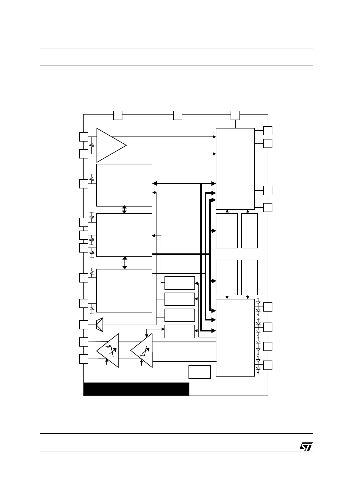
BLOCK DIAGRAM
WDP
WDN
FLT
VCC (+5V) VGND (0V) VEE (-5V)
PREDRIVER
3v
FAULT PROCESSOR
Low supply detection,
Open/short heads,
TA detection,
low write frequency,
high temperature
HW0P
HW0N
WRITE
DRIVERS
HW1/5P
SDATA
SCLK
SEN
R/W
MRR
ABHV/
ADTV
RDP
RDN
3v
SERIAL INTERFACE
3v
HEAD SELECTION
MODE CONTROL
Gain boost,
Low pass filter
CONTROL
&
High pass
filter
Imr, Iwr
RW enable
head select
A2D
RMR, te mp
ABHV,
MR meas
Temperature
monitoring
TA detection,
TA correction
VREF
WRITE
DAC
READ
DAC
MR
READ
INPUT
STAGES
HW1/5N
Rdamp
Overshoot,
Undershhot
low bias
current/voltage
HR0P
HR0N
HR1/5P
HR1/5N
2/4
L6327/L6332 6/ 4 CH

L6327 - L6332
DIM.
mm inch
MIN. TYP. MAX. MIN. TYP. MAX.
A 1.10 0.043
A1 0.05 0.15 0.002 0.006
A2 0.85 0.90 0.95 0.033 0.035 0.037
b 0.17 0.27 0 .007 0.011
c 0.09 0.20 0.0035 0.008
D 9.60 9.70 9.80 0.378 0.382 0.386
E 6.40 0.252
e 0.50 0.020
E1 4.30 4.40 4.50 0.169 0.173 0.177
L 0.50 0.60 0.70 0.020 0.024 0.028
k 0˚ (m in.) 8˚ (m ax.)
OUTLINE AND
MECHANICAL DATA
TSSOP38
Thin Shrink Small Outline Package
0.010 mm
0.004 inch
SEATING PLANE
38 20
Pin 1 identification
be
D
19
A2
A1
E
A
SEATING PLANE
A1
E1
c
Gage Plane
0.25mm
k
L
TSSO3 8M
3/4

L6327 - L6332
Information furnished is believed to be accurate and reliable. However, STMicroelectronics assumes no responsibility for the consequences
of use of such information nor for any infringement of patents or other rights of third parties which may result from its use. No license is granted
by implic ation or otherwise under any patent or p atent rights of STMicroelectr oni cs. Specifications mentioned in thi s publicati on are subject
to change without notice. This publication supersedes and replaces all information previously supplied. STMicroelectronics products are not
authorized for use as cri tical comp onents in life support devi ces or systems without express writt en approval o f STM i croelectr o nics.
The ST logo is a registered trademark of STMicroelectronics
2001 STMi croelectronics - All Ri ghts Rese rved
Australi a - Brazil - Chin a - Finland - Franc e - Germany - Hon g Ko ng - India - Italy - Japan - Malays i a - M al ta - Morocco - Sin gapore - S pain
STMicroelectronics GROUP OF COMPANIES
- Sweden - Sw itzerlan d - United Kin gdom - U.S.A.
http://www.s t. com
4/4
 Loading...