

high current DMOS universal motor driver
Features
■ Able to drive both windings of a bipolar stepper
motor or two DC motors
■ Output current up to 1.3A each winding
■ Wide voltage range: 12V to 40V
■ Four quadrant current control, ideal for
microstepping and DC motor control
■ Precision PWM control
■ No need for recirculation diodes
■ TTL/CMOS compatible inputs
■ Cross conduction protection
■ Thermal shutdow
Description
L6258EP is a dual full bridge for motor control
applications realized in BCD technology, with the
capability of driving both windings of a bipolar
stepper motor or bidirectionally control two DC
motors.
L6258EP
PWM controlled
PowerSSO36
The power stage is a dual DMOS full bridge
capable of sustaining up to 40V, and includes the
diodes for current recirculation. The output current
capability is 1.3A per winding in continuous mode,
with peak start-up current up to 2A. A thermal
protection circuitry disables the outputs if the chip
temperature exceeds the safe limits.
L6258EP and a few external components form a
complete control and drive circuit. It has high
efficiency phase shift chopping that allows a very
low current ripple at the lowest current control
levels, and makes this device ideal for steppers as
well as for DC motors.
Table 1. Device summary
Order code Package Packing
E-L6258EP PowerSSO36 Tube
December 2007 Rev 4 1/32
www.st.com
1

Contents L6258EP
Contents
1 Block diagram . . . . . . . . . . . . . . . . . . . . . . . . . . . . . . . . . . . . . . . . . . . . . . 5
2 Functional description . . . . . . . . . . . . . . . . . . . . . . . . . . . . . . . . . . . . . . 10
2.1 Reference voltage . . . . . . . . . . . . . . . . . . . . . . . . . . . . . . . . . . . . . . . . . . 11
2.2 Input logic (I0 - I1 - I2 - I3) . . . . . . . . . . . . . . . . . . . . . . . . . . . . . . . . . . . . 12
2.3 Phase input ( PH ) . . . . . . . . . . . . . . . . . . . . . . . . . . . . . . . . . . . . . . . . . . 13
2.4 Triangular generator . . . . . . . . . . . . . . . . . . . . . . . . . . . . . . . . . . . . . . . . . 13
2.5 Charge pump circuit . . . . . . . . . . . . . . . . . . . . . . . . . . . . . . . . . . . . . . . . . 13
2.6 Current control loop . . . . . . . . . . . . . . . . . . . . . . . . . . . . . . . . . . . . . . . . . 14
2.7 Current control loop compensation . . . . . . . . . . . . . . . . . . . . . . . . . . . . . 15
3 PWM current control loop . . . . . . . . . . . . . . . . . . . . . . . . . . . . . . . . . . . 16
3.1 Open loop transfer function analysis . . . . . . . . . . . . . . . . . . . . . . . . . . . . 16
3.2 Power amplifier . . . . . . . . . . . . . . . . . . . . . . . . . . . . . . . . . . . . . . . . . . . . . 17
3.3 Load attenuation . . . . . . . . . . . . . . . . . . . . . . . . . . . . . . . . . . . . . . . . . . . . 18
3.4 Error amplifier and sense amplifier . . . . . . . . . . . . . . . . . . . . . . . . . . . . . . 19
3.5 Effect of the Bemf on the current control loop stability . . . . . . . . . . . . . . . 22
4 Application information . . . . . . . . . . . . . . . . . . . . . . . . . . . . . . . . . . . . . 24
4.1 Interference . . . . . . . . . . . . . . . . . . . . . . . . . . . . . . . . . . . . . . . . . . . . . . . 24
4.2 Motor selection . . . . . . . . . . . . . . . . . . . . . . . . . . . . . . . . . . . . . . . . . . . . . 25
4.3 Unused inputs . . . . . . . . . . . . . . . . . . . . . . . . . . . . . . . . . . . . . . . . . . . . . 25
4.4 Notes on PCB design . . . . . . . . . . . . . . . . . . . . . . . . . . . . . . . . . . . . . . . . 26
5 Operation mode time diagrams . . . . . . . . . . . . . . . . . . . . . . . . . . . . . . . 27
6 Package information . . . . . . . . . . . . . . . . . . . . . . . . . . . . . . . . . . . . . . . . 30
7 Revision history . . . . . . . . . . . . . . . . . . . . . . . . . . . . . . . . . . . . . . . . . . . 31
2/32

L6258EP List of tables
List of tables
Table 1. Device summary . . . . . . . . . . . . . . . . . . . . . . . . . . . . . . . . . . . . . . . . . . . . . . . . . . . . . . . . . . 1
Table 2. Absolute maximum rating . . . . . . . . . . . . . . . . . . . . . . . . . . . . . . . . . . . . . . . . . . . . . . . . . . . 5
Table 3. Pin functions . . . . . . . . . . . . . . . . . . . . . . . . . . . . . . . . . . . . . . . . . . . . . . . . . . . . . . . . . . . . . 6
Table 4. Electrical characteristics . . . . . . . . . . . . . . . . . . . . . . . . . . . . . . . . . . . . . . . . . . . . . . . . . . . . 8
Table 5. Current levels . . . . . . . . . . . . . . . . . . . . . . . . . . . . . . . . . . . . . . . . . . . . . . . . . . . . . . . . . . 12
Table 6. Charge pump capacitor's values. . . . . . . . . . . . . . . . . . . . . . . . . . . . . . . . . . . . . . . . . . . . . 13
Table 7. Document revision history . . . . . . . . . . . . . . . . . . . . . . . . . . . . . . . . . . . . . . . . . . . . . . . . . 31
3/32

List of figures L6258EP
List of figures
Figure 1. Block diagram . . . . . . . . . . . . . . . . . . . . . . . . . . . . . . . . . . . . . . . . . . . . . . . . . . . . . . . . . . . . 5
Figure 2. Pin connection (top view) . . . . . . . . . . . . . . . . . . . . . . . . . . . . . . . . . . . . . . . . . . . . . . . . . . . 6
Figure 3. Power bridge configuration . . . . . . . . . . . . . . . . . . . . . . . . . . . . . . . . . . . . . . . . . . . . . . . . . 11
Figure 4. Current control loop block diagram. . . . . . . . . . . . . . . . . . . . . . . . . . . . . . . . . . . . . . . . . . . 12
Figure 5. Output comparator waveforms . . . . . . . . . . . . . . . . . . . . . . . . . . . . . . . . . . . . . . . . . . . . . . 14
Figure 6. Ax bode plot . . . . . . . . . . . . . . . . . . . . . . . . . . . . . . . . . . . . . . . . . . . . . . . . . . . . . . . . . . . . 19
Figure 7. Aloop bode plot (uncompensated) . . . . . . . . . . . . . . . . . . . . . . . . . . . . . . . . . . . . . . . . . . . 20
Figure 8. Aloop bode plot (compensated) . . . . . . . . . . . . . . . . . . . . . . . . . . . . . . . . . . . . . . . . . . . . . 22
Figure 9. Electrical model of the load. . . . . . . . . . . . . . . . . . . . . . . . . . . . . . . . . . . . . . . . . . . . . . . . . 23
Figure 10. Typical application circuit . . . . . . . . . . . . . . . . . . . . . . . . . . . . . . . . . . . . . . . . . . . . . . . . . . 25
Figure 11. Full step operation mode timing diagram . . . . . . . . . . . . . . . . . . . . . . . . . . . . . . . . . . . . . . 27
Figure 12. Half step operation mode timing diagram . . . . . . . . . . . . . . . . . . . . . . . . . . . . . . . . . . . . . . 28
Figure 13. 4 bit microstep operation mode timing diagram . . . . . . . . . . . . . . . . . . . . . . . . . . . . . . . . . 29
Figure 14. PowerSSO36 mechanical data & package dimensions . . . . . . . . . . . . . . . . . . . . . . . . . . . 30
4/32
L6258EP Block diagram
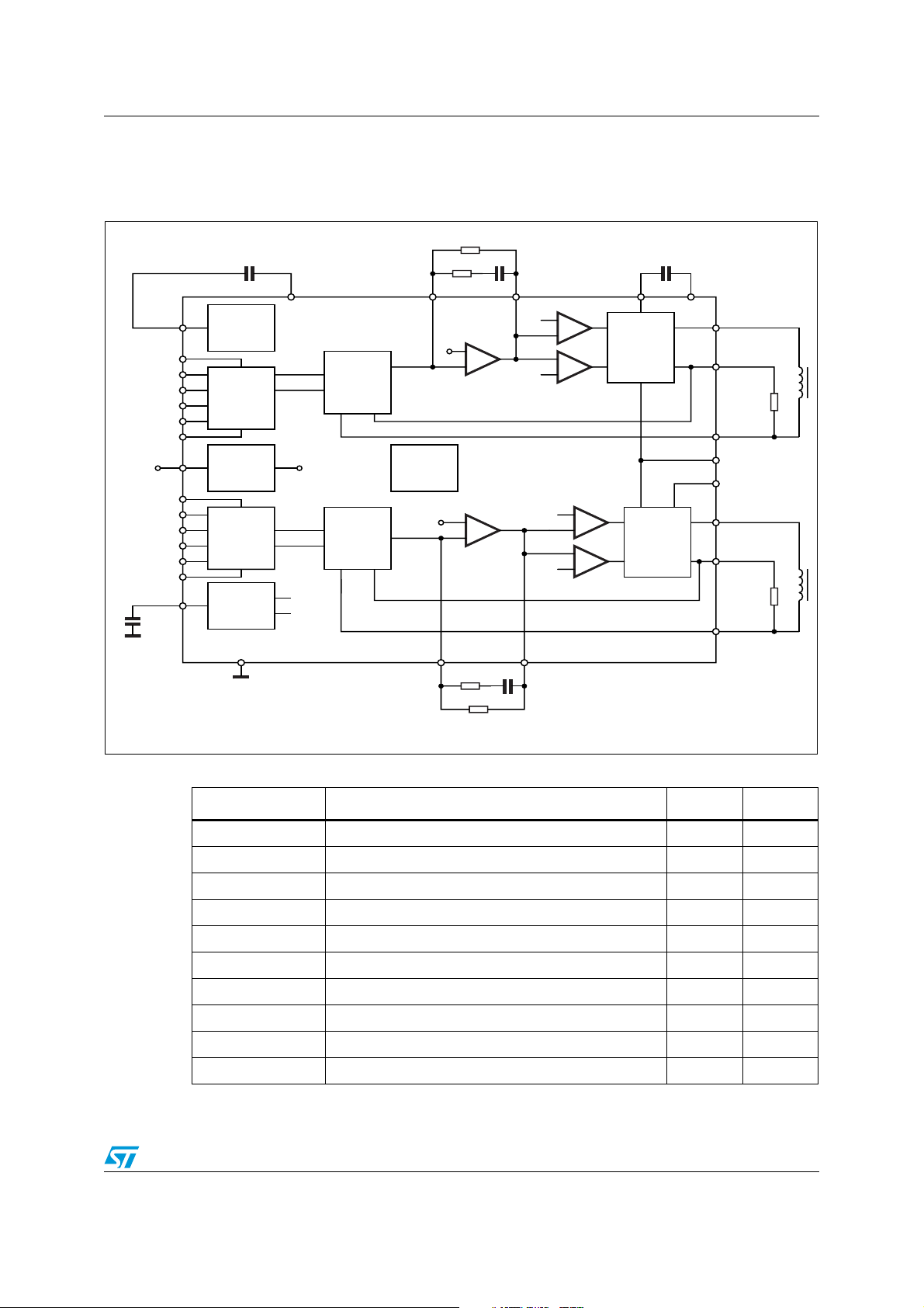
1 Block diagram
Figure 1. Block diagram
R
1M
VDD(5V)
TRI_CAP
VCP1
VREF1
I3_1
I2_1
I1_1
I0_1
PH_1
VREF1
I3_2
I2_2
I1_2
I0_2
PH_2
C
FREF
C
P
CHARGE
PUMP
DAC
VR GEN
DAC
TRIANGLE
GENERATOR
VR (VDD/2)
TRI_0
TRI_180
INPUT
&
SENSE
AMP
INPUT
&
SENSE
AMP
EA_IN1 EA_OUT1VCP2
THERMAL
PROT.
1
C
C1
R
C1
TRI_0
+
C
TRI_0
TRI_180
-
+
C
-
+
C
-
+
C
-
ERROR
V
R
AMP
+
TRI_180
-
ERROR
V
R
AMP
+
-
VS
POWER
BRIDGE
C
1
POWER
BRIDGE
2
BOOT
VBOOT
OUT1A
OUT1B
SENSE1B
SENSE1A
DISABLE
VS
OUT2A
OUT2B
SENSE2B
SENSE2A
R
s
R
s
EA_IN2 EA_OUT2GND
R
R
Table 2. Absolute maximum rating
C2
C
C2
1M
2
D96IN430D
Parameter Description Value Unit
V
s
V
DD
V
ref1/Vref2
I
O
I
O
V
in
V
boot
- V
V
boot
s
T
j
T
stg
1. This current is intended as not repetitive current for max. 1 second.
Supply voltage 45 V
Logic supply voltage 7 V
Reference voltage 2.5 V
Output current (peak)
(1)
2A
Output current (continuous) 1.3 A
Logic input voltage range -0.3 to 7 V
Bootstrap supply 60 V
Maximum Vgate applicable 15 V
Junction temperature 150 °C
Storage temperature range -55 to 150 °C
5/32
Block diagram L6258EP
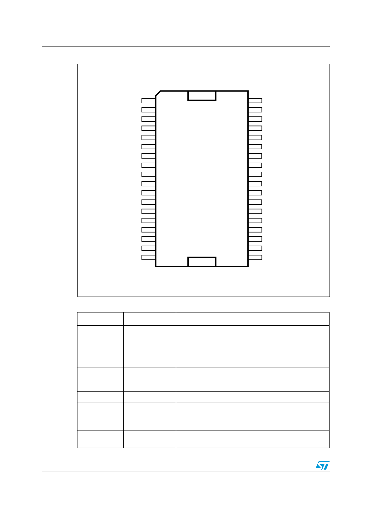
Figure 2. Pin connection (top view)
PWR_GND
PH_1
I1_1
I0_1
OUT1A
DISABLE
TRI_CAP
V
CC
GND
VCP1
VCP2
VBOOT
VS
OUT2A
I0_2
I1_2
PH_2
PWR_GND
1
2
3
4
5
6
7
8
9
10 27
11
12
13 24
14
15
16
17
18
D96IN432E
36
35
34
33
32
31
30
29
28
26
25
23
22
21
20
19
PWR_GND
SENSE1
OUT1B
I3_1
I2_1
VS
EA_OUT1
EA_IN1
VREF1
SIG_GND
VREF2
EA_IN2
EA_OUT2
I2_2
I3_2
OUT2B
SENSE2
PWR_GND
Table 3. Pin functions
Pin # Name Description
1, 36 PWR_GND
Ground connection (1). They also conduct heat from die to
printed circuit copper.
These TTL compatible logic inputs set the direction of
2, 17 PH_1, PH_2
current flow through the load. A high level causes current to
flow from OUTPUT A to OUTPUT B.
Logic input of the internal DAC (1). The output voltage of the
3I
1_1
DAC is a percentage of the Vref voltage applied according to
the thruth Table 5 on page 12.
4I
0_1
See pin 3
5 OUT1A Bridge output connection (1)
6 DISABLE
7TRI_cap
Disables the bridges for additional safety during switching.
When not connected the bridges are enabled
Triangular wave generation circuit capacitor. The value of
this capacitor defines the output switching frequency
6/32

L6258EP Block diagram
Table 3. Pin functions (continued)
Pin # Name Description
8V
(5V) Supply voltage input for logic circuitry
DD
9 GND Power ground connection of the internal charge pump circuit
10 V
11 V
12 V
13, 31 V
CP1
CP2
BOOT
S
Charge pump oscillator output
Input for external charge pump capacitor
Overvoltage input for driving of the upper DMOS
Supply voltage input for output stage. They are shorted
internally
14 OUT2A Bridge output connection (2)
Logic input of the internal DAC (2). The output voltage of the
15 I
0_2
DAC is a percentage of the VRef voltage applied according
to the truth Table 5 on page 12
16 I
1_2
18, 19 PWR_GND
See pin 15
Ground connection. They also conduct heat from die to
printed circuit copper
20, 35 SENSE2, SENSE1 Negative input of the transconductance input amplifier (2, 1)
21 OUT2B
22 I
23 I
3_2
2_2
Bridge output connection and positive input of the
tranconductance (2)
See pin 15
See pin 15
24 EA_OUT_2 Error amplifier output (2)
25 EA_IN_2 Negative input of error amplifier (2)
Reference voltages for the internal DACs, determining the
26, 28 V
REF2
, V
REF1
output current value. Output current also depends on the
logic inputs of the DAC and on the sensing resistor value
27 SIG_GND Signal ground connection
29 EA_IN_1 Negative input of error amplifier (1)
30 EA_OUT_1 Error amplifier output (1)
32 I
33 I
2_1
3_1
34 OUT1B
See pin 3
See pin 3
Bridge output connection and positive input of the
tranconductance (1)
Note: The number in parenthesis shows the relevant Power Bridge of the circuit. Pins 18, 19, 1
and 36 are connected together.
7/32
Block diagram L6258EP
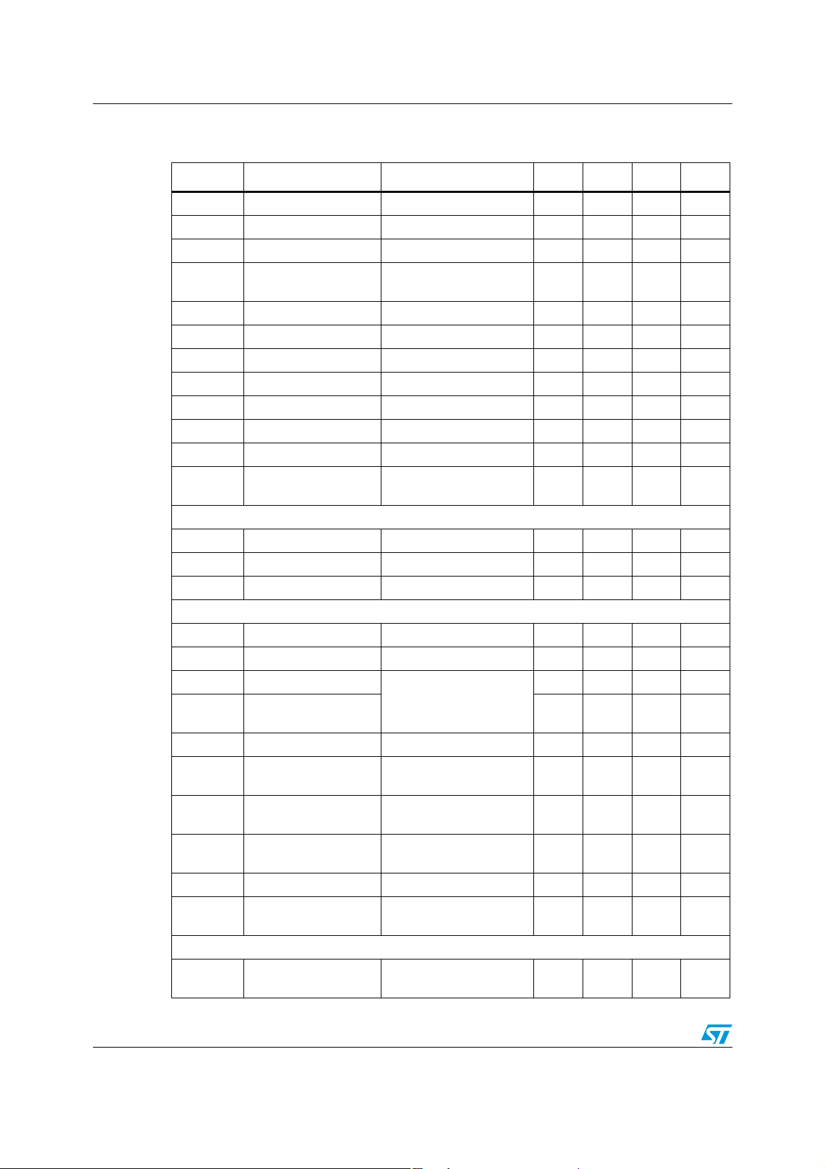
Table 4. Electrical characteristics
(V
= 40V; VDD = 5V; Tj = 25°; unless otherwise specified.)
S
Parameter Description Test condition Min. Typ. Max. Unit
V
V
V
BOOT
V
Sense
V
S(off)
V
DD(off)
I
S(on)
I
S(off)
I
ΔT
T
f
DD
DD
SD-H
SD
osc
Supply voltage 12 40 V
S
Logic supply voltage 4.75 5.25 V
Storage voltage VS = 12 to 40V VS+6 VS+12 V
Max drop across sense
resistor
Power off reset Off threshold 6 7.2 V
Power off reset Off threshold 3.3 4.1 V
VS quiescent current Both bridges ON, no load 15 mA
VS quiescent current Both bridges OFF 7 mA
VDD operative current 15 mA
Shut down hysteresis 25 °C
Thermal shutdown 150 °C
Triangular oscillator
frequency
TRANSISTORS
I
R
DSS
ds(on)
V
Leakage current OFF State 500 μA
On resistance ON state 0.6 0.75 W
Flywheel diode voltage If =1.0A 1 1.4 V
f
CONTROL LOGIC
V
in(H)
V
in(L)
I
in
I
dis
V
ref1/ref2
I
ref
FI =
V
ref/Vsense
V
FS
V
offset
lnput voltage All Inputs 2 V
Input voltage All inputs 0 0.8 V
Input current
Disable pin input
current
Reference voltage Operating 0 2.5 V
V
terminal input
ref
current
PWM loop transfer
ratio
DAC full scale
precision
Current loop offset V
DAC factor ratio
SENSE AMPLIFIER
(1)
(2)
1.25 V
C
= 1nF 12.5 15 18.5 KHz
FREF
DD
-150 +10 μA
0 < Vin < 5V
-10 +150 μA
= 1.25 -2 5 μA
V
ref
2
= 2.5V I0/I1/I2/I3 = L 1.23 1.34 V
V
ref
= 2.5V I0/I1/I2/I3 = H -40 +40 mV
ref
Normalized @ full scale
value
-2 +2 %
V
V
cm
lnput common mode
voltage range
8/32
-0.7 V
+0.7 V
S

L6258EP Block diagram
Table 4. Electrical characteristics (continued)
(V
= 40V; VDD = 5V; Tj = 25°; unless otherwise specified.)
S
Parameter Description Test condition Min. Typ. Max. Unit
I
inp
Input bias sense1/sense2 -200 0 μA
ERROR AMPLIFIER
G
Open loop voltage gain 70 dB
V
SR Output slew rate Open loop 0.2 V/μs
GBW
1. Chopping frequency is twice fosc value.
2. This is true for all the logic inputs except the disable input.
Gain bandwidth
product
400 kHz
9/32

Functional description L6258EP
2 Functional description
The circuit is intended to drive both windings of a bipolar stepper motor or two DC motors.
The current control is generated through a switch mode regulation.
With this system the direction and the amplitude of the load current are depending on the
relation of phase and duty cycle between the two outputs of the current control loop.
The L6258EP power stage is composed by power DMOS in bridge configuration as it is
shown in Figure 3, where the bridge outputs OUT_A and OUT_B are driven to V
high level at the inputs IN_A and IN_B while are driven to ground with a low level at the
same inputs.
The zero current condition is obtained by driving the two half bridge using signals IN_A and
IN_B with the same phase and 50% of duty cycle.
In this case the outputs of the two half bridges are continuously switched between power
supply (V
) and ground, but keeping the differential voltage across the load equal to zero.
s
In Figure 3 is shown the timing diagram of the two outputs and the load current for this
working condition.
Following we consider positive the current flowing into the load with a direction from OUT_A
to OUT_B, while we consider negative the current flowing into load with a direction from
OUT_B to OUT_A.
with an
s
Now just increasing the duty cycle of the IN_A signal and decreasing the duty cycle of IN_B
signal we drive positive current into the load.
In this way the two outputs are not in phase, and the current can flow into the load trough the
diagonal bridge formed by T1 and T4 when the output OUT_A is driven to V
and the output
s
OUT_B is driven to ground, while there will be a current recirculation into the higher side of
the bridge, through T1 and T2, when both the outputs are at Vs and a current recirculation
into the lower side of the bridge, through T3 and T4, when both the outputs are connected to
ground.
Since the voltage applied to the load for recirculation is low, the resulting current discharge
time constant is higher than the current charging time constant during the period in which
the current flows into the load through the diagonal bridge formed by T1 and T4. In this way
the load current will be positive with an average amplitude depending on the difference in
duty cycle of the two driving signals.
In Figure 3 is shown the timing diagram in the case of positive load current
On the contrary, if we want to drive negative current into the load is necessary to decrease
the duty cycle of the IN_A signal and increase the duty cycle of the IN_B signal. In this way
we obtain a phase shift between the two outputs such to have current flowing into the
diagonal bridge formed by T2 and T3 when the output OUT_A is driven to ground and
output OUT_B is driven to Vs, while we will have the same current recirculation conditions of
the previous case when both the outputs are driven to Vs or to ground.
So, in this case the load current will be negative with an average amplitude always
depending by the difference in duty cycle of the two driving signals.
In Figure 3 is shown the timing diagram in the case of negative load current.
Figure 4 shows the device block diagram of the complete current control loop.
10/32
 Loading...